
1 Analog Frontend for Multichannel Neuronal Recording...
9
1 Analog Frontend for Multichannel Neuronal Recording System with Spike and LFP Separation Yevgeny Perelman and Ran Ginosar, VLSI Systems Research Center, Department of Electrical Engineering, Technion–Israel Institute of Technology, Haifa 32000, Israel [email protected], [email protected] Abstract? We have to think of some I. I NTRODUCTION Recent advances in fabrication of MEMS microelectrode arrays [1], [2], together with the ability of coupling the arrays directly to VLSI chips, allow simultaneous monitoring of tens and even hundreds of neurons. Moreover, clinical applications of brain-machine interfaces may require monitoring of much larger populations, even hundreds and thousands of neurons [3]. With this large a number of recording units, communicating raw neuronal signals results in prohibitively large data rates [4]. When sampled with 20Ksps, eight bit precision, even a hundred of electrodes would generate 16Mbps, too large for common methods of low-power wireless communications. Evidently, some form of data reduction must be applied prior to communication. It is possible to detect the presence of neuronal spikes as demonstrated in [4] and communicate only active portions of recorded signals. Assuming an electrode might ”sense” two or three units which fire 20 times per second on average, and taking the firing event length to be 2mSec, only ten times data rate reduction can be achieved. Further reduction can be provided by restricting the communicated information to mere indications of spike presence. January 4, 2005 DRAFT
-
Upload
phungtuong -
Category
Documents
-
view
213 -
download
0
Transcript of 1 Analog Frontend for Multichannel Neuronal Recording...

1
Analog Frontend for Multichannel Neuronal
Recording System
with Spike and LFP Separation
Yevgeny Perelman and Ran Ginosar,
VLSI Systems Research Center, Department of Electrical Engineering,
Technion–Israel Institute of Technology, Haifa 32000, Israel
[email protected], [email protected]
Abstract?
We have to think of some
I. INTRODUCTION
Recent advances in fabrication of MEMS microelectrode arrays [1], [2], together with the
ability of coupling the arrays directly to VLSI chips, allow simultaneous monitoring of tens and
even hundreds of neurons. Moreover, clinical applications of brain-machine interfaces may require
monitoring of much larger populations, even hundreds and thousands of neurons [3].
With this large a number of recording units, communicating raw neuronal signals results in
prohibitively large data rates [4]. When sampled with 20Ksps, eight bit precision, even a hundred
of electrodes would generate 16Mbps, too large for common methods of low-power wireless
communications. Evidently, some form of data reduction must be applied prior to communication.
It is possible to detect the presence of neuronal spikes as demonstrated in [4] and communicate
only active portions of recorded signals. Assuming an electrode might ”sense” two or three units
which fire 20 times per second on average, and taking the firing event length to be 2mSec, only
ten times data rate reduction can be achieved. Further reduction can be provided by restricting
the communicated information to mere indications of spike presence.
January 4, 2005 DRAFT
ran
Cross-Out
ran
Rectangle
ran
Rectangle

2
An extracellular microelectrode typically senses activity from several units adjacent to its tip.
Spike sorting [5] applies classification techniques to assign spike waveforms of different shapes
to different units. With on-chip spike sorting, the data bandwidth is reduced to 200Kbps (almost
a hundred times) for the figures above, assuming a 32bit message generated for every spike.
Another reason for on-chip sorting is brought in [6]. In autonomous motor prosthetics, as-
suming that every spike coming from a certain electrode is generated by the same unit might
prove not sufficiently accurate enough for movement trajectory calculations. [6] shows also that
implementation of existing algorithms for on chip spike sorting is feasible in terms of power
dissipation.
Motivation of this work
In a signal recorded by an extracellular microelectrode, neuronal firing activity occupies the
100-10.000Hz frequency band; its amplitude is typically lower than 500µV . The Local Field
Potential (LFP) occupies the lower frequencies, below 100Hz, with amplitudes below 5mV. The
signal-to-noise ratio of the combined signal is rather large: as the microelectrode noise [7] and
background noise of cortical activity [8] are typically 5µV , it may reach 60dB.
Since the LFP must be filtered out prior to spike sorting, it is possible to block it right at
the front-end [9], by high-pass filtering below 100Hz. It was shown, however, that LFP carries
important information [10], [11]. Several front-end circuits pass the LFP band intact: [12], [13],
[14]. They block the large input DC offsets, typical for neuronal signals, by high-pass filtering
below 1Hz. As the entire combined signal is passed, the minimal required precision of subsequent
data acquisition is 10 bit, defined by the signal SNR. The maximal gain is limited by the LFP
magnitude and chip supply voltage. Since the firing activity (SPK) has ten timer lower magnitude
than the LFP, it can be amplified only to one tenth of the output swing.
To overcome these limitations, we suggest splitting the signal into two bands after the first
amplification stage. Thus, the LFP and SPK parts can be processed by separate channels, am-
plifying both to the full swing. Consequently, the system dynamic ange needs only be a 100,
as determined by the SNR of the SPK signal. Thus, no more than seven bits data acquisition is
required.
In this paper we present an integrated CMOS front-end for neuronal recordings from implanted
electrodes capable of delivering both spike data and the local field potential from twelve true-
differential recording channels. The front-end is intended for further integration on a head-stage
with an external wireless interface.
Following the overall system architecture along with some basic parameter constraints and the
preamp circuit, the paper presents the measurement results of the fabricated test chip.
January 4, 2005 DRAFT

3
II. ARCHITECTURE
A 0.35µm CMOS twelve-channel neuronal recording front-end IC was designed with a true-
differential inputs, so that each electrode can be referenced to any point in the system. The
amplification channel was designed to have an RMS noise level of 2-3µV in the band of 0.2-
10kHz.
The block diagram of a single channel is shown in Fig. 1.
x100buf
DA
C
Reg
DA
C
Reg
VGA
VGAx10
LFP
LPF SPK
freq. splitter
DATA<4:0>
RD, WR, ADDR
GSPK<1:0>GLFP<1:0> FSPK<2:0>
neg
pos
NULL
high pass filter
Fig. 1. A single channel block diagram
The input signal is first cleared of the DC offsets by a single-pole input high-pass filter. The
corner frequency should be of several Hertz, in order to pass the LFP part of the signal intact.
The resistors (8MΩ ) were placed on-chip, whereas the capacitors must be added extrnally. As
the IC was intended to couple to 0.1-1MΩ electrodes, 8MΩ input resistance should not present
too much of a load.
The first stage provides an amplification of 40dB to a single-ended output, which is band-split
by a first-order RC filter into high frequency SPK (neuronal firing activity) and low frequency
LFP parts. The splitter pole was roughly placed at 200Hz, by using a 5MΩ resistor (high-resistive
poly) and 160pF (gate-oxide) capacitor.
The minimal gain to be provided by the first stage is determined by noise constraints as
follows. RMS noise introduced by the resistor into the signal (at room temperature) is:√
4kTRf0 = 28µV
assuming the output LPF has a steep roll-off above f0 =10kHz. The first stage gain is required to
be well above 20dB in order to keep the input referred noise of the high splitter resistance below
3µV . First stage gain of 40dB was taken as a design goal.
January 4, 2005 DRAFT

4
The low frequency LFP signal is amplified by a variable-gain amplifier (VGA) and buffered to
chip outputs. The VGA provides digitally selectable gains of 2.5/5/7.5/10x. Thus, the maximum
total gain of the LFP channel was designed to be 60dB.
The high frequency SPK signal is amplified by a factor of ten and by another VGA (to a
total maximum of 80dB). Its upper corner frequency is limited by a second-order Bessel LPF,
implemented (for the sake of simplicity) as a continuous time Sallen-Key RC biquad [16]. Resistors
are implemented as serially-connected polysilicon segments, which can be selectively shortened
by means of a three-bit controlling signal. Filter cutoff can be varied that way in the range of
8.5-13kHz.
Although successful implementation of a neuronal signal processing channel based on switched
capacitor filter has been reported [9], we have decided to design continuous-time analog circuits,
to avoid contaminating the input with switching noise. Switched capacitor implementation for
filters can provide for better time-constant accuracy and smaller area, neither of which was our
main design goal.
DC offsets of both the SPK and LFP channels have to be compensated: LFP channel amplifies
the input preamp offset (hundreds of µV , typically) by up to 60dB; unless compensated, it would
limit the dynamic range severely or even saturate the VGA. SPK channel offset is determined
by the offset of the x10 stage amplified by 40dB, as the DC part of the preamp output signal is
cut off by the band splitter. Smaller than LFP, preamp offset is yet significant: the x10 stage has
larger input offset compared to the preamp, since the latter uses very large input devices due to
the noise requirements.
Offset compensation is carried out by two calibration DACs (one for LFP, one for SPK)
applied to the last amplification stages (VGAs). The DACs are implemented as 5-stage R2R
resistor ladders, having 400mV output swing. DAC values are stored in registers that can be
individually accessed by the controller FSM through a common bus with five address/data bits
and three control bits. The controller calibrates the outputs, one by one, upon de-assertion of the
RST signal (Fig. 2).
III. INPUT PREAMPLIFIER
The input preamplifier must provide a sufficiently high input impedance in order not to overload
the high-impedance recording electrode. The noise level requirement is dictated by the inherent
noise of the recording electrode and cortical background noise, both of which having magnitude
of several µV . In addition, the preamp must have a flat frequency response starting from DC and
use no switching circuits. A differential circuit addressing the above requirements is shown on
Fig. 3.
January 4, 2005 DRAFT

5
CH#1SPK
LFP
CH#2SPK
LFP
CH#3SPK
LFP
MUX
RST
CLK
Controller
chip outputs
ADDR,RD,WR
DATA<4:0>
Fig. 2. Chip architecture
This is a degenerated differential cascoded transconductor stage, loaded with a resistor to
convert the output current back to voltage. The disadvantage of this circuit is the gain error due
to the finite transconductance of input transistors. The gain of the circuit on Fig. 3 is given by:
A =2R
r + rm
=2R/r
1 + rm/r
where rm is the transresistance of M1,2. While r can be matched to R by using the same resistor
types and employing appropriate layout techniques, there is no straightforward way of matching
r to rm. The sensitivity to rm can be reduced by reducing the ratio rm/r, but there is a limit
on how high r can be due to the noise requirements (some 10kΩ ) and reducing rm means more
power.
Instead, we match r to rm by appropriately controlling the bias currents through M1,2. M1,2
are operated in the subthreshold region (the smallest rm for a given Id) so that rm is inversely
proportional to Id:
rm =ηVth
Id
, Vth =kT
q
Id is given by:
Id =Vdd − Vgs3
rb
thus we can write the gain as:
A =2R
r + rbηVth
Vdd−Vgs3
January 4, 2005 DRAFT

6
vdd
vss
posrb
r r
R
negM1 M2
M3
bias
Fig. 3. Input preamplifier circuit topology
We match rb to r and keep Vgs3 much lower than Vdd. Since the ratio of Vth and Vdd is small,
the above expression becomes weakly dependent on process parameter η and on Vgs3. The chip
is expected to work in constant temperatures (subject body), thus the dependence on Vth is not
worrying. One sigma chip-to-chip channel gain variation of less than 2% was actually measured.
IV. MEASUREMENT RESULTS
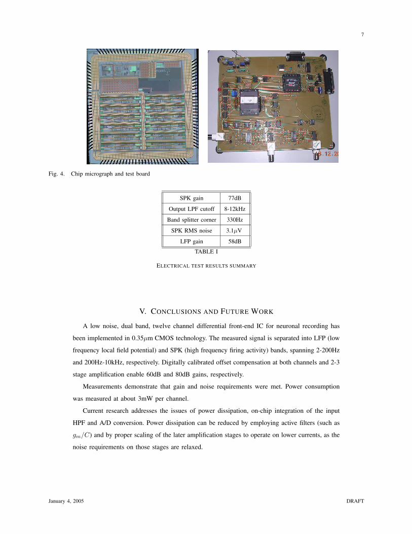
The chip was fabricated using AMS 0.35µm quad-metal, double poly CMOS process with
3.3V power supply (Fig. 4).
Ten fabricated chips were tested electrically. Some of the electrical test results are summarized
in Tab. I. While most of the design goals were met, note that band splitter frequency is somewhat
displaced. This is due to a failure in the band-splitter MOS capacitor biasing circuit.
The measured frequency response (magnitude) for SPK and LFP bands is shown in Fig. 5 (a).
The frequency response is quite stable over all the measured chips. Fig. 5 (b) shows input-referred
noise power spectral density (PSD) of several channels together with a simulated curve (solid line).
1/f noise dominates over the LFP band and thermal noise dominates the higher frequency SPK
band. The increase at the high end is due to out of band components (i.e. above the output LPF
cutoff). Power dissipation of 3mW per channel was measured.
January 4, 2005 DRAFT
7
Fig. 4. Chip micrograph and test board
SPK gain 77dB
Output LPF cutoff 8-12kHz
Band splitter corner 330Hz
SPK RMS noise 3.1µV
LFP gain 58dB
TABLE I
ELECTRICAL TEST RESULTS SUMMARY
V. CONCLUSIONS AND FUTURE WORK
A low noise, dual band, twelve channel differential front-end IC for neuronal recording has
been implemented in 0.35µm CMOS technology. The measured signal is separated into LFP (low
frequency local field potential) and SPK (high frequency firing activity) bands, spanning 2-200Hz
and 200Hz-10kHz, respectively. Digitally calibrated offset compensation at both channels and 2-3
stage amplification enable 60dB and 80dB gains, respectively.
Measurements demonstrate that gain and noise requirements were met. Power consumption
was measured at about 3mW per channel.
Current research addresses the issues of power dissipation, on-chip integration of the input
HPF and A/D conversion. Power dissipation can be reduced by employing active filters (such as
gm/C) and by proper scaling of the later amplification stages to operate on lower currents, as the
noise requirements on those stages are relaxed.
January 4, 2005 DRAFT

8
101 102 103 104 105 1060
10
20
30
40
50
60
70
Gai
n [d
B20
]
F [Hz]
SPIKE & LFP transfer, chip#1, ch#4
(a) Frequency response (b) Input noise PSD. Black line —
simulated PSD.Fig. 5. Measured channel frequency response and input-referred noise PSD
REFERENCES
[1] Q. Bai, K. D. Wise, and D. J. Anderson, “A high-yield microassembly structure for three-dimensional
microelectrode arrays,” IEEE Trans. Biomed Eng., vol. 47, no. 3, pp. 281–289, March 2000.
[2] E. M. Maynard, C. T. Nordhausen, and R. Normann, “The utah intracortical electrode array: a
recording structure for potential brain-computer interfaces,” Electroencephalography and clinical
Neurophysiology, vol. 102, pp. 228–239, 1997.
[3] M. Nicolelis, “Actions from thoughts,” Nature, vol. 409, pp. 403–407, 2001.
[4] R. R. Harrison, “A low-power integrated circuit for adaptive detection of action potentials in noisy
signals,” in Proc. of the 25-th Annual International Conference of the IEEE EMBS, September 2003,
pp. 3325–3328.
[5] M. S. Lewicki, “A review of methods for spike sorting: the detection and classification of neural action
potentials,” Network: Computation in Neural Systems, vol. 9, no. 4, pp. R53–R78, 1998.
[6] Z. S. Zumsteg, R. E. Ahmed, G. Santhanam, K. V. Shenoy, and T. H. Meng, “Power feasibility of
implantable digital spike-sorting circuits for neural prosthetic systems,” in Proc. of the 26-th Annual
International Conference of the IEEE EMBS, September 2004, pp. 4237–4240.
[7] D. A. Borkholder, “Cell based biosensors using microelectrodes,” Ph.D. dissertation, Univ. of Stanford,
Novermber 1998.
[8] K. Guillory and R. Normann, “A 100-channel system for real time detection and storage of extracellular
spike waveforms,” Journal of Neuroscience Methods, vol. 91, pp. 21–29, 1999.
[9] I. Obeid, J. C.Morizio, M. A. L. N. K. A. Moxon, and P. D. Wolf, “Two multichannel integrated circuits
for neural recording and signal processing,” IEEE Trans. on Biomed. Eng., vol. 50, no. 2, pp. 255–258,
February 2003.
[10] A. Arieli, A. Sterkin, A. Grinvald, and A. Aertsen, “Dynamics of ongoing activity: Explanation of the
large variability in evoked cortical responses,” Science, vol. 273, pp. 1868–1871, September 1996.
January 4, 2005 DRAFT

9
[11] J. P. DONOGHUE, J. N. SANES, N. G. HATSOPOULOS, and G. GAAL, “Neural discharge and
local field potential oscillations in primate motor cortex during voluntary movements,” The Journal of
Neurophysiology, vol. 79, no. 1, pp. 159–173, January 1998.
[12] R. R. Harrison and C. Charles, “A low-power low-noise cmos amplifier for neural recording applica-
tions,” IEEE Journal of Solid State Circuits, vol. 38, no. 6, pp. 958–965, June 2003.
[13] W. R. Patterson, Y. K. Song, C. W. Bull, I. Ozden, A. P. Deangellis, C. Lay, J. L. McKay, A. V.
Nurmikko, J. D. Donoghue, and B. W. Connors, “A microelectrode/microelectronic hybrid device for
brain implantable neuroprosthesis applications,” IEEE Trans. on Biomed. Eng., vol. 51, no. 10, October
2004.
[14] P. Mohseni and K. Najafi, “A fully integrated neural recording amplifier with dc input stabilization,”
IEEE Trans. on Biomed. Eng., vol. 51, no. 5, May 2001.
[15] R. Lemon, Methods For Neuronal Recording In Conscious Animals. International Brain Research
Organization, 1984.
[16] T. L. Deliyannis, Y. Sun, and J. K. Fidler, Continuous-Time Active Filter Design. CRC Press, 1999.
January 4, 2005 DRAFT