1 An overview of work in Glasgow relevant to the design study Stuart Reid 1 SUPA, University of...
25
1 An overview of work in Glasgow relevant to the design study Stuart Reid Stuart Reid 1 SUPA, University of Glasgow SUPA, University of Glasgow Glasgow University – 22 July 2010 Glasgow University – 22 July 2010
-
Upload
antonia-ball -
Category
Documents
-
view
215 -
download
0
Transcript of 1 An overview of work in Glasgow relevant to the design study Stuart Reid 1 SUPA, University of...
1
An overview of work in Glasgow relevant to the design study
Stuart ReidStuart Reid11 SUPA, University of Glasgow SUPA, University of Glasgow
Glasgow University – 22 July 2010Glasgow University – 22 July 2010

Materials issues for ETMaterials issues for ET
22
• The construction of a 3rd generation gravitational wave observatory within Europe E.T. (Einstein Telescope).
• Cryogenic operating temperature (ET-LF)– Silicon proposed as test mass and suspension material + construction/bonding– Identification of best mirror coatings material/technology being investigated
1 10 100 1000 1000010
-25
10-24
10-23
10-22
10-21
10-20
10-19
Frequency [Hz]
3rd generationS
train
[H
z-1/2
]
1st generation
2nd generation
Seismic/suspension/
Newtonian Noise
Thermal Noise
Shot Noise

33
• Single layers of coating materials appliedto silicon cantilever substrates supplied by Stanford / KNT (Glasgow)
• Cantilever clamped rigidly and bending modes excited electrostatically.• Loss calculated from envelope of exponential decay in amplitude
Multilayer mirror coatingsMultilayer mirror coatings
coated cantilever in clamp
tantala coating
electrostaticdrive
34mm
500m50m thick
Coating applied here

44
• Comparison of dissipation in tantala doped with 14.5 % TiO2 and un-doped tantala for 3rd (left) and 4th (right) bending modes.
• TiO2 doping reduces the height and slightly increases the width of the dissipation peak
• TiO2 doping reduces the loss of Ta2O5 throughout the temperature range studied, with the exception of the wings of the peak
Effect of doping on loss of TaEffect of doping on loss of Ta22OO55 coatings coatings
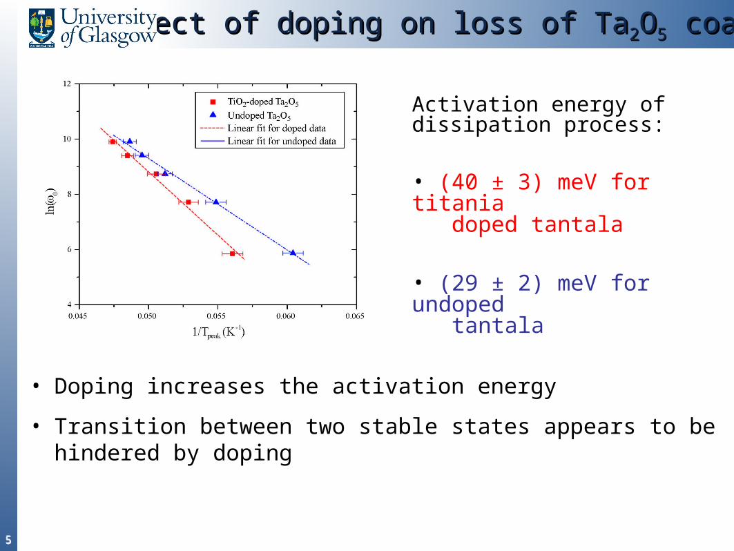
55
• Doping increases the activation energy
• Transition between two stable states appears to be hindered by doping
Effect of doping on loss of TaEffect of doping on loss of Ta22OO55 coatings coatings
Activation energy of dissipation process:
• (40 ± 3) meV for titania doped tantala
• (29 ± 2) meV for undoped tantala
66
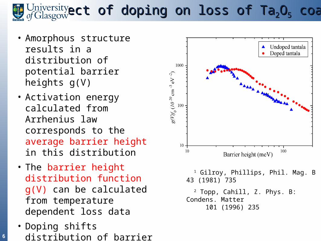
Effect of doping on loss of TaEffect of doping on loss of Ta22OO55 coatings coatings
• Amorphous structure results in a distribution of potential barrier heights g(V)
• Activation energy calculated from Arrhenius law corresponds to the average barrier height in this distribution
• The barrier height distribution function g(V) can be calculated from temperature dependent loss data
• Doping shifts distribution of barrierheights to higher energy, thusreducing loss
1 Gilroy, Phillips, Phil. Mag. B 43 (1981) 735
2 Topp, Cahill, Z. Phys. B: Condens. Matter 101 (1996) 235

77
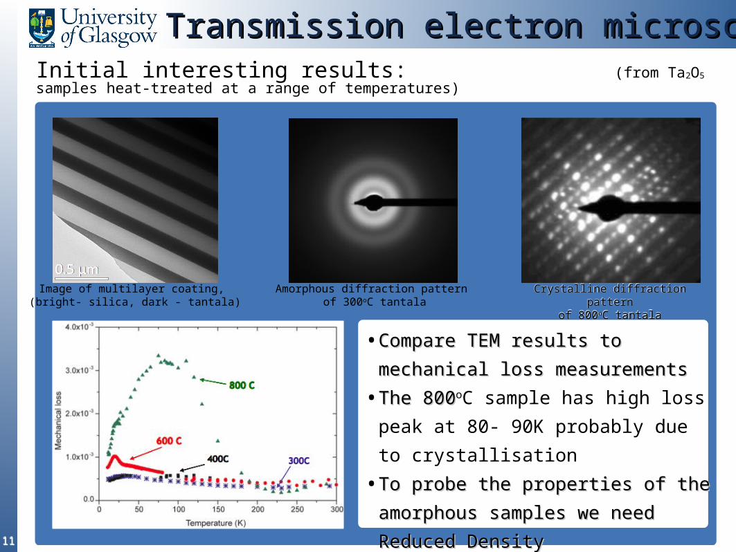
Effect of heat treatment temperature on TaEffect of heat treatment temperature on Ta22OO55 loss loss
• 35 K peak: Observed in Ta2O5 heat treated at 300, 400 C. Evidence suggests may also be present in Ta2O5 heat treated at 600 C. Activation energy 54 meV (postulate that this may be analogous to dissipation peak in fused silica, involving thermally activated transitions of oxygen atoms)
• 18K peak: Observed in Ta2O5 heat treated at 600 C and 800 C. Dissipation mechanism may be related to structural changes brought on by heat treatment close to re-crystallisation temperature. Perhaps the start of pre-crystallisation ordering (but still appears amorphous on electron diffraction measurements)
• 90K peak: Observed in coating heat treated at 800 C. Large, broad loss peak likely to be related to (expected) onset of polycrystalline structure due to high temperature heat treatment. Dissipation mechanism could be e.g. phonon scattering at grain boundaries – more analysis required
800 C
Above: Electron diffraction pattern of Ta2O5 heat treated at 800 C
Left: Loss at 1.9 kHz of 0.5 m Ta2O5 coatings annealed at 300, 400, 600 and 800 C.
88
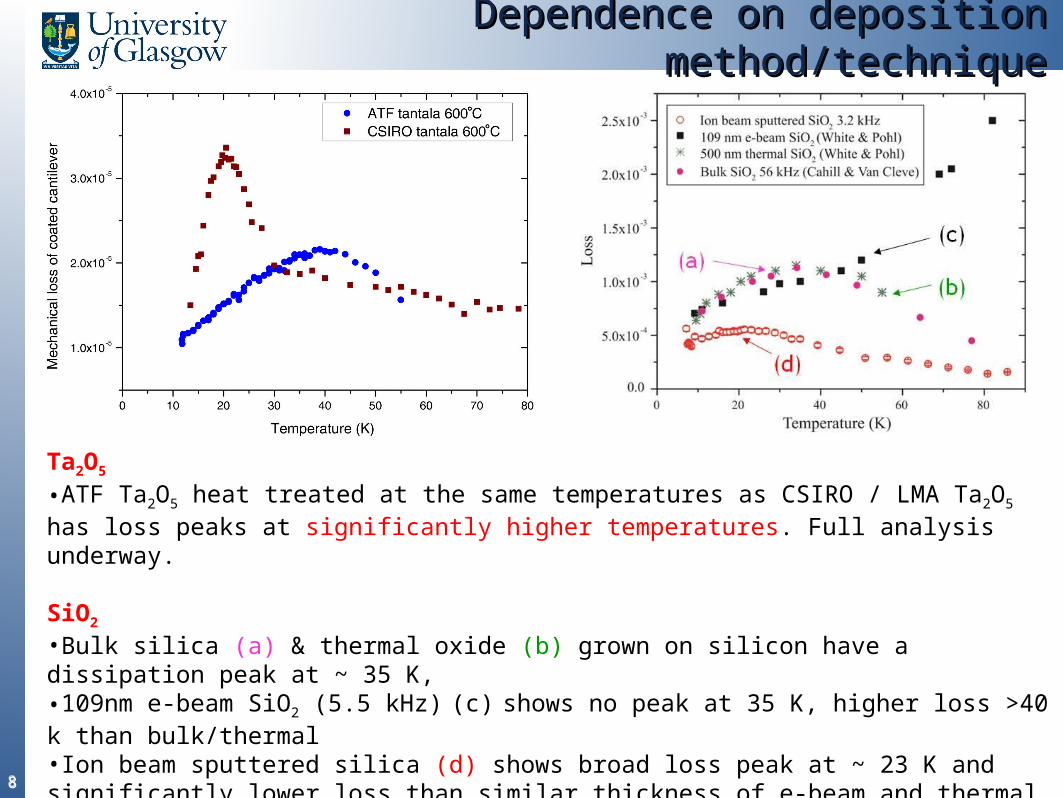
Dependence on deposition method/techniqueDependence on deposition method/technique
Ta2O5
•ATF Ta2O5 heat treated at the same temperatures as CSIRO / LMA Ta2O5 has loss peaks at significantly higher temperatures. Full analysis underway.
SiO2
•Bulk silica (a) & thermal oxide (b) grown on silicon have a dissipation peak at ~ 35 K,•109nm e-beam SiO2 (5.5 kHz) (c) shows no peak at 35 K, higher loss >40 k than bulk/thermal•Ion beam sputtered silica (d) shows broad loss peak at ~ 23 K and significantly lower loss than similar thickness of e-beam and thermal SiO2
Suggests details of coating deposition procedure may have significant impact on the temperature dependence of the mechanical loss – further study of great interest!

99
Alternative high-index coating materialsAlternative high-index coating materials
HfO2
• Different atomic weight/size (differences in dynamics arising from atomic weight)
• Loss lower than tantala below 125 K
• Peak position (50 K) and width shifted compared to tantala (no peak in 100 C data)
• High optical absorption (60 ppm) measured at Stanford
• Electron diffraction measurements show evidence of both crystalline and amorphous structure in all the hafnia coatings
• Silica-doped hafnia remains amorphous when annealed up to 500 C, and presence of silica appears to only slightly increase loss at room temperature

1010
• Useful for probing atomic structure and chemistry
• Allows us to characterise atomic structure– Imaging– Diffraction – Spectroscopy
Studying the atomic structure of IBS coatingsStudying the atomic structure of IBS coatings
What is causing the What is causing the mechanical loss on an mechanical loss on an
atomic level?atomic level?
1111
Image of multilayer coating, (bright- silica, dark - tantala)
Amorphous diffraction pattern of 300oC tantala
Crystalline diffraction patternof 800oC tantala
Crystalline diffraction patternof 800oC tantala
• Compare TEM results to mechanical loss Compare TEM results to mechanical loss
measurementsmeasurements• The 800The 800oC sample has high loss peak at 80-
90K probably due to crystallisation• To probe the properties of the amorphous To probe the properties of the amorphous
samples we need Reduced Density samples we need Reduced Density
FunctionsFunctions
Initial interesting results: (from Ta2O5 samples heat-treated at a range of temperatures)
Transmission electron microscopyTransmission electron microscopy

1212
Reduced density functionsReduced density functions
• The reduced density function is a Fourier transform of the information gained from the intensity profile [D. J. H. Cockayne, Annu.Rev.Mater.Res, 37:159-87, (2007)]
Intensity profile Reduced density functionTantala diffraction pattern
• Silica and tantala are amorphous materials– They do not have long range order– They do have short range order
• We can probe this short range order with reduced density functions– RDFs give a statistical representation of where atoms sit with regards to a central atom
1313
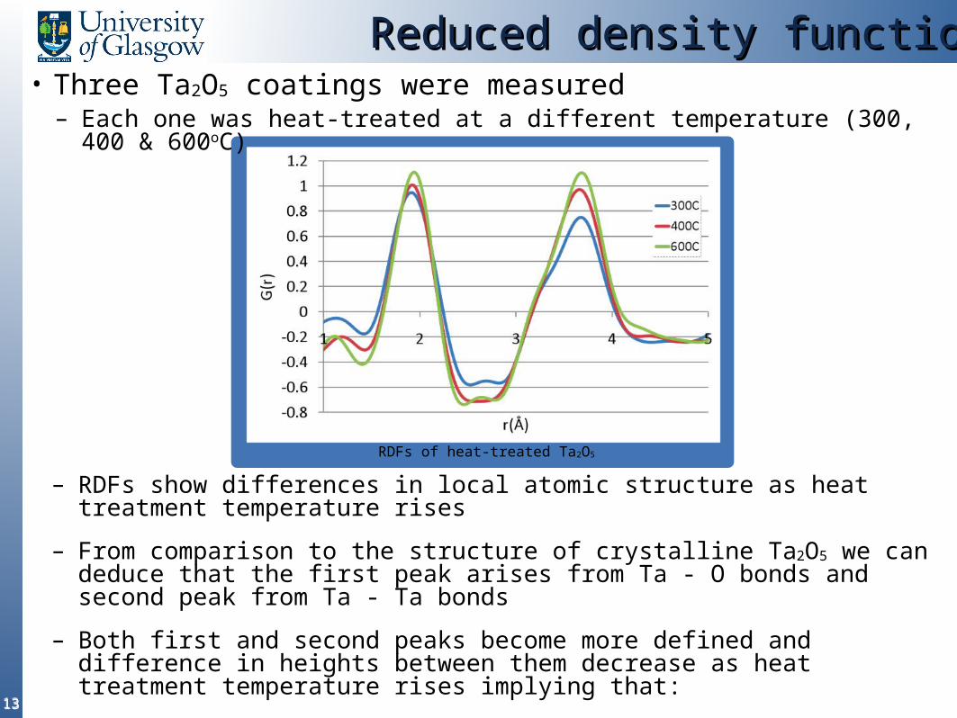
Reduced density functionsReduced density functions
RDFs of heat-treated Ta2O5
• Three Ta2O5 coatings were measured– Each one was heat-treated at a different temperature (300, 400 & 600oC)
– RDFs show differences in local atomic structure as heat treatment temperature rises
– From comparison to the structure of crystalline Ta2O5 we can deduce that the first peak arises from Ta - O bonds and second peak from Ta - Ta bonds
– Both first and second peaks become more defined and difference in heights between them decrease as heat treatment temperature rises implying that:
– Material is becoming more ordered– There is an increase in Ta - Ta bonding

1414
Modelling the atomic structureModelling the atomic structure
Atomic model of amorphous Ta2O5 with red coloured
oxygen and blue coloured tantalum atoms from molecular dynamics
simulations showing a stable Ta2O2 fragment
(a) Comparison between refined and experimental RDFs, (b) partial RDFs
showing individual nearest neighbourdistances within the model
•Atomic structure measurements from this model provides important information including nearest atomic neighbour distances, co-ordination numbers and observed similarities between crystalline and amorphous phases, such as clusters with increased contribution from a Ta2O2 ring fragment.

1515
Diffractive optics and waveguide coatingsDiffractive optics and waveguide coatings
•Proposals have been made that potentially allow a significant reduction in the coating thickness required for high reflectivity in future GW detectors, e.g. diffractive optics and waveguide coatings.
•Both can be fabricated through micromachining silicon surfaces
300nm
400nm
1um
Waveguide coating fabricated in JenaSimple grating pattern with comparable geometryto Jena waveguides, fabricated in Glasgow (KNT)

1616
Diffractive optics and waveguide coatingsDiffractive optics and waveguide coatings
•Initial results comparing cantilevers with and without grating structures can be seen below (results for the 5th bending mode at ~3kHz)•Preliminary measurements suggest that the increased surface area (top surface area increased ~3x), resulting from the grating pattern, have an insignificant effect on the overall measured mechanical loss of our cantilevers.•Further gratings with reduced period (more lines) are currently being fabricated in Glasgow.•T-shaped (waveguide) gratings are ready in Jena for measuring.•A collaborative effort to characterise the thermal noise of waveguide coatings is underway.
1717
Construction quasi-monolithic silicon suspensionsConstruction quasi-monolithic silicon suspensions
•Requirements for 3rd generation GW observatories (ET-LF / low T)
•Bond thermomechanical properties- Thermal noise (mechanical loss + thickness)- Heat extraction (thermal conductivity + bond area)
•Bond robustness- Mechanical strength- Temperature cycling effects/failures

1818
Hydroxide-catalysis bond thicknessHydroxide-catalysis bond thickness
•SEM imaging of the bond material
Si
Si
SiO2
SiO2
Bond material
40 nm
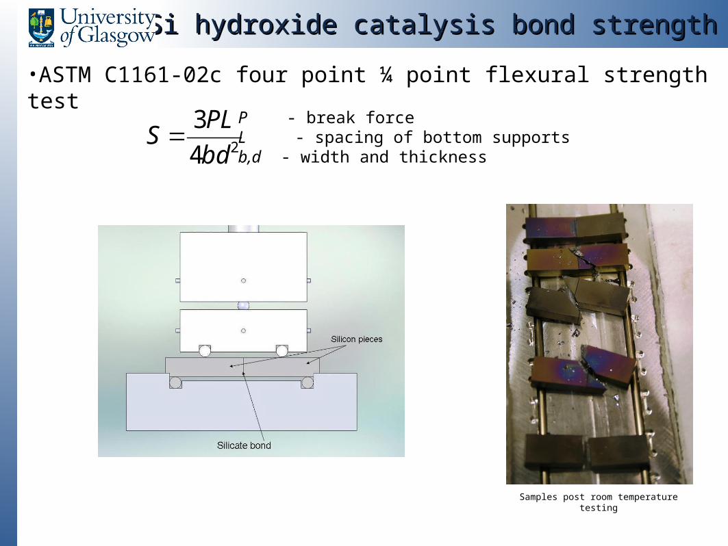
Si-Si hydroxide catalysis bond strength testingSi-Si hydroxide catalysis bond strength testing
•ASTM C1161-02c four point ¼ point flexural strength test
24
3
bd
PLS
P - break forceL - spacing of bottom supportsb,d - width and thickness
Samples post room temperature testing

Si-Si hydroxide catalysis bond strength testingSi-Si hydroxide catalysis bond strength testing
0 50 100 150 200 250 3000
10
20
30
40
50
60
70
Minimum oxide layer of sample [nm]
Str
engt
h [M
pa]
Cryogenic Temperature ResultsRoom Temperature Results

Si – Si Hydroxide Catalysis Bonds - temperature cyclingSi – Si Hydroxide Catalysis Bonds - temperature cycling
The ability of silicate bonds to withstand repeated temperature cycles must be verified, in addition to withstanding the thermal stresses that may be induced during cooling.
Repeated cycles from room temperature to 77K were performed on bonded samples of silicon with no bond failures (in addition to this various samples of different materials including SiO2-ZnSe, SiO2-Ge, SiO2-ULE, SiO2 Al‐ 2O3, all of whom have different coeff. of thermal expansion)

Si – Si Hydroxide Catalysis Bonds - thermal conductivitySi – Si Hydroxide Catalysis Bonds - thermal conductivity
Florence results
Thermal conductivity measurements carried out by Matteo LorenziniBonded silicon sample fabricated in Glasgow (1” diameter, 28 + 48 mm lengths)Thermal conductivity of bonded sample at low T peak similar to modeled pure silicon with thin (~700nm) glass-like layer
Heat flow
BO
NDTmeas Tmeas Tmeas
Lorenzini et al., ET meeting, 1-3 March 2010, Friedrich-Schiller-Universität Jena.
http://www.et-gw.eu/

Si – Si Hydroxide Catalysis Bonds - thermal conductivitySi – Si Hydroxide Catalysis Bonds - thermal conductivity
ATC/Glasgow thermal conductivity investigations:
•Preliminary thermal conductance measurements have been carried out between the UK Astronomy Technology Centre (Edinburgh) and Glasgow.•Plan to study the dependence of the thermal conductivity as a function of thermal oxide layer thickness.
Figure 3: Thermal Conductance vs. Temperature for bulk (reference) and bonded samples with standard deviation errors. The sample follows the form G=aTb where here the values for the bulk and bonded sample
a=2.65 ± 0.97 and 0.27 ± 0.01 and b= 1.01 ± 0.19 and 1.29 ± 0.01 respectively, with temperature T.
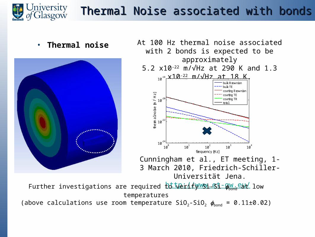
Thermal Noise associated with bondsThermal Noise associated with bonds
• Thermal noise
Cunningham et al., ET meeting, 1-3 March 2010, Friedrich-Schiller-
Universität Jena.http://www.et-gw.eu/
At 100 Hz thermal noise associated with 2 bonds is expected to be
approximately5.2 x10-22 m/√Hz at 290 K and 1.3 x10⁻²²
m/√Hz at 18 K.
100
101
102
103
104
10-24
10-22
10-20
10-18
frequency [Hz]th
erm
al n
ois
e [m
/ H
z]
bulk Brownianbulk TEcoating Browniancoating TEcoating TRtotal
Further investigations are required to verify Si-Si bond at low temperatures(above calculations use room temperature SiO2-SiO2 bond = 0.11±0.02)

Summary of bonding work in GlasgowSummary of bonding work in Glasgow
Silicate bonding appears to be a highly promising technique for the construction of cryogenic and ultra-low loss monolithic suspensions
Ongoing collaborative research: Characterisation of mechanical loss at low T Thermal conductivity measurements below 37 K Establishing the effect of the type of oxide layer Technique/chemistry used to achieve bond and how it affect
thermomechanical properties