1 A very low drop voltage regulator · April 2017 DocID025502 Rev 2 1/33 This is information on a...
33
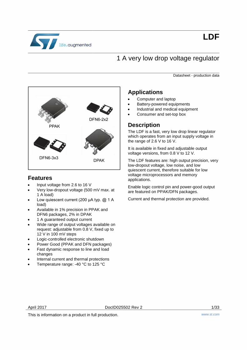
April 2017 DocID025502 Rev 2 1/33 This is information on a product in full production. www.st.com LDF 1 A very low drop voltage regulator Datasheet - production data Features Input voltage from 2.6 to 16 V Very low-dropout voltage (500 mV max. at 1 A load) Low quiescent current (200 μA typ. @ 1 A load) Available in 1% precision in PPAK and DFN6 packages, 2% in DPAK 1 A guaranteed output current Wide range of output voltages available on request: adjustable from 0.8 V, fixed up to 12 V in 100 mV steps Logic-controlled electronic shutdown Power Good (PPAK and DFN packages) Fast dynamic response to line and load changes Internal current and thermal protections Temperature range: -40 °C to 125 °C Applications Computer and laptop Battery-powered equipments Industrial and medical equipment Consumer and set-top box Description The LDF is a fast, very low drop linear regulator which operates from an input supply voltage in the range of 2.6 V to 16 V. It is available in fixed and adjustable output voltage versions, from 0.8 V to 12 V. The LDF features are: high output precision, very low-dropout voltage, low noise, and low quiescent current, therefore suitable for low voltage microprocessors and memory applications. Enable logic control pin and power-good output are featured on PPAK/DFN packages. Current and thermal protection are provided.
Transcript of 1 A very low drop voltage regulator · April 2017 DocID025502 Rev 2 1/33 This is information on a...
April 2017 DocID025502 Rev 2 1/33
This is information on a product in full production. www.st.com
LDF
1 A very low drop voltage regulator
Datasheet - production data
Features Input voltage from 2.6 to 16 V
Very low-dropout voltage (500 mV max. at 1 A load)
Low quiescent current (200 μA typ. @ 1 A load)
Available in 1% precision in PPAK and DFN6 packages, 2% in DPAK
1 A guaranteed output current
Wide range of output voltages available on request: adjustable from 0.8 V, fixed up to 12 V in 100 mV steps
Logic-controlled electronic shutdown
Power Good (PPAK and DFN packages)
Fast dynamic response to line and load changes
Internal current and thermal protections
Temperature range: -40 °C to 125 °C
Applications Computer and laptop
Battery-powered equipments
Industrial and medical equipment
Consumer and set-top box
Description The LDF is a fast, very low drop linear regulator which operates from an input supply voltage in the range of 2.6 V to 16 V.
It is available in fixed and adjustable output voltage versions, from 0.8 V to 12 V.
The LDF features are: high output precision, very low-dropout voltage, low noise, and low quiescent current, therefore suitable for low voltage microprocessors and memory applications.
Enable logic control pin and power-good output are featured on PPAK/DFN packages.
Current and thermal protection are provided.
Contents LDF
2/33 DocID025502 Rev 2
Contents
1 Block diagram .................................................................................. 3
2 Pin configuration ............................................................................. 4
3 Typical application .......................................................................... 5
4 Absolute maximum ratings ............................................................. 6
5 Electrical characteristics ................................................................ 7
6 Application information ................................................................ 11
6.1 External capacitors .......................................................................... 11
6.1.1 Input capacitor .................................................................................. 11
6.1.2 Output capacitor ............................................................................... 11
6.2 Output voltage setting for ADJ version ............................................ 11
6.3 Enable pin operation ....................................................................... 11
6.4 Power Good .................................................................................... 11
7 Typical characteristics .................................................................. 12
8 Package information ..................................................................... 16
8.1 DFN6 (3x3) package information .................................................... 16
8.2 DFN6 (3x3) packing information ...................................................... 18
8.3 DFN6 (2x2) package information .................................................... 20
8.4 DFN6 (2x2) packing information ...................................................... 23
8.5 PPAK package information ............................................................. 24
8.6 DPAK package information ............................................................. 26
8.7 PPAK and DPAK packing information ............................................. 29
9 Ordering information ..................................................................... 31
10 Revision history ............................................................................ 32
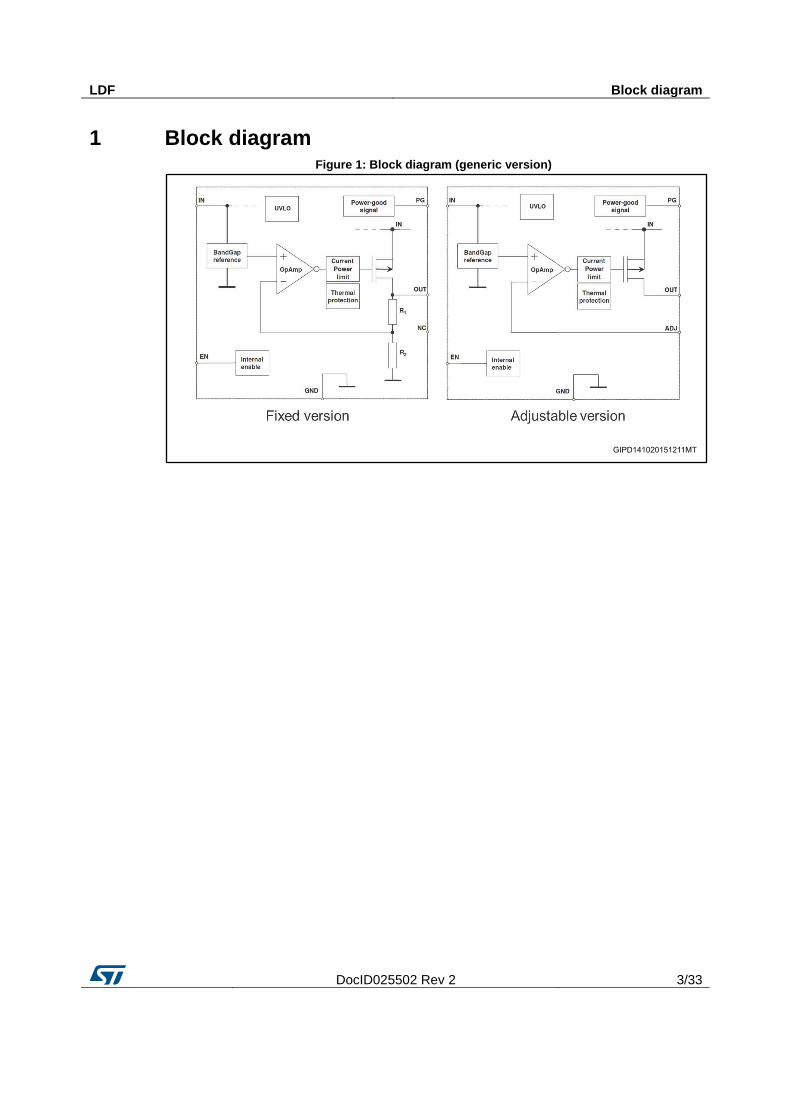
LDF Block diagram
DocID025502 Rev 2 3/33
1 Block diagram Figure 1: Block diagram (generic version)
Pin configuration LDF
4/33 DocID025502 Rev 2
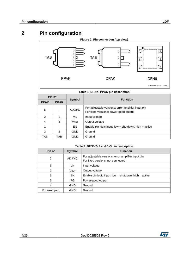
2 Pin configuration Figure 2: Pin connection (top view)
Table 1: DPAK, PPAK pin description
Pin n° Symbol Function
PPAK DPAK
5 - ADJ/PG For adjustable versions: error amplifier input pin
For fixed versions: power-good output
2 1 VIN Input voltage
4 3 VOUT Output voltage
1 - EN Enable pin logic input: low = shutdown, high = active
3 2 GND Ground
TAB TAB GND Ground
Table 2: DFN6-2x2 and 3x3 pin description
Pin n° Symbol Function
2 ADJ/NC For adjustable versions: error amplifier input pin
For fixed versions: not connected
6 VIN Input voltage
1 VOUT Output voltage
5 EN Enable pin logic input: low = shutdown, high = active
3 PG Power-good output
4 GND Ground
Exposed pad GND Ground

LDF Typical application
DocID025502 Rev 2 5/33
3 Typical application Figure 3: Fixed versions
Figure 4: Adjustable versions (PPAK and DFN6 packages only)
Absolute maximum ratings LDF
6/33 DocID025502 Rev 2
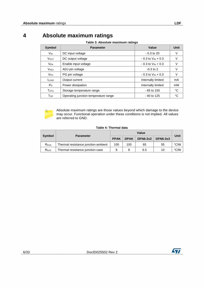
4 Absolute maximum ratings Table 3: Absolute maximum ratings
Symbol Parameter Value Unit
VIN DC input voltage - 0.3 to 20 V
VOUT DC output voltage - 0.3 to VIN + 0.3 V
VEN Enable input voltage - 0.3 to VIN + 0.3 V
VADJ ADJ pin voltage -0.3 to 2 V
VPG PG pin voltage - 0.3 to VIN + 0.3 V
ILOAD Output current Internally limited mA
PD Power dissipation Internally limited mW
TSTG Storage temperature range - 65 to 150 °C
TOP Operating junction temperature range - 40 to 125 °C
Absolute maximum ratings are those values beyond which damage to the device may occur. Functional operation under these conditions is not implied. All values are referred to GND.
Table 4: Thermal data
Symbol Parameter Value
Unit PPAK DPAK DFN6-2x2 DFN6-3x3
RthJA Thermal resistance junction-ambient 100 100 65 55 °C/W
RthJC Thermal resistance junction-case 8 8 6.5 10 °C/W
LDF Electrical characteristics
DocID025502 Rev 2 7/33
5 Electrical characteristics
TJ = 25 °C, VIN = VOUT(NOM) + 1 V, CIN = 1 μF, COUT = 2.2 μF, ILOAD = 10 mA, VEN = 2 V, unless otherwise specified.
Table 5: LDF (fixed versions) electrical characteristics
Symbol Parameter Test conditions Min. Typ. Max. Unit
VIN Operating input voltage
2.6
16 V
VOUT VOUT accuracy, PPAK and DFN6 versions
VOUT +1 V (1) ≤ VIN ≤ 16 V ILOAD = 10 mA
-1
1 %
10 mA ≤ ILOAD ≤ 1 A
TJ = -40 to 125 °C -1.5
1.5 %
VOUT VOUT accuracy, DPAK version
VOUT +1 V (1) ≤ VIN ≤ 16 V ILOAD = 10 mA
-2
2 %
10 mA ≤ ILOAD ≤ 1 A
TJ = -40 to 125 °C -3
3 %
ΔVOUT Static line regulation
VOUT +1 V (1) ≤ VIN ≤ 16 V
0.01
%V VOUT +1 V (1) ≤ VIN ≤ 16 V
TJ = -40 to 125 °C 0.04
ΔVOUT Static load regulation
10 mA ≤ ILOAD ≤ 1 A
0.2
%/A 10 mA ≤ ILOAD ≤ 1 A
TJ = -40 to 125 °C 0.6
VDROP Dropout voltage (2) ILOAD = 1 A
-40 °C < TJ < 125 °C 200 500 mV
Iq Quiescent current
ON mode: VEN = 2 V
ILOAD = 10 mA to 1 A
TJ = -40 to 125 °C
200 800
µA OFF mode: VEN = GND, PPAK and DFN versions
30
OFF mode: VEN = GND, PPAK and DFN versions
-40 °C < TJ < 125 °C
120
ISC Short-circuit current VIN > 3 V
1.5
A
VEN Enable input logic low VIN = 2.6 V to 16 V
-40 °C < TJ < 125 °C
0.8 V
Enable input logic high 2
IEN Enable pin input current
VEN = VIN
5 10 µA
PG
Power-good output threshold
Rising edge
0.92*VOUT
V Falling edge
0.8*VOUT
Power-good output voltage low
ISINK = 6 mA
open drain output 0.4

Electrical characteristics LDF
8/33 DocID025502 Rev 2
Symbol Parameter Test conditions Min. Typ. Max. Unit
SVR Supply voltage rejection
VIN = 4.5 V +/- 0.5 VRIPPLE f = 120 Hz
VOUT = 3.3 V
60
dB VIN = 4.5 V +/- 0.5 VRIPPLE
f = 120 Hz to 100 kHz VOUT = 3.3 V
45
eN Output noise voltage
Bw = 10 Hz to 100 kHz, ILOAD = 100 mA
COUT = 2.2 μF
45
μVRMS /VOUT
TSHDN Thermal shutdown
170
°C Hysteresis
10
Notes:
(1) For VOUT < 1.6 V; VIN = 2.6 V. (2) Dropout voltage is the input-to-output voltage difference at which the output voltage is 100 mV below its nominal value. This specification does not apply to output voltages below 1.6 V.
LDF Electrical characteristics
DocID025502 Rev 2 9/33
TJ = 25 °C, VIN = VOUT(NOM) + 1 V, CIN = 1 μF, COUT = 2.2 μF, ILOAD = 10 mA, VEN = 2 V, unless otherwise specified.
Table 6: LDF (adjustable version) electrical characteristics
Symbol Parameter Test conditions Min. Typ. Max. Unit
VIN Operating input voltage
2.6
16 V
VADJ
Reference voltage VIN = VOUT +1 V (1)
0.8
V
Reference voltage tolerance
VOUT + 1 V (1) ≤ VIN ≤ 16 V
ILOAD = 10 mA -1
1
% 10 mA ≤ ILOAD ≤ 1 A
TJ = -40 to 125 °C -1.5
1.5
ΔVOUT Static line regulation
VOUT +1 V (1) ≤ VIN ≤ 16 V
0.01
%V VOUT+1 V (1) ≤ VIN ≤ 16 V
TJ = -40 to 125 °C 0.04
ΔVOUT Static load regulation
10 mA ≤ ILOAD ≤ 1 A
0.2
%/A
10 mA ≤ ILOAD ≤ 1 A
TJ = -40 to 125 °C 0.2 0.6
VDROP Dropout voltage (2)
VOUT fixed to 2.5 V,
ILOAD = 1 A
-40 °C < TJ < 125 °C
200 500 mV
Iq Quiescent current
ON mode: VEN = 2 V
ILOAD = 10 mA to 1 A
TJ = -40 to 125 °C
200 800
µA OFF mode: VEN = GND
PPAK and DFN versions 30
OFF mode: VEN = GND
PPAK and DFN versions
-40 °C < TJ < 125 °C
120
ISC Short-circuit current VIN > 3 V
1.5
A
VEN
Enable input logic low VIN = 2.6 V to 16 V
-40 °C < TJ < 125 °C
0.8
V Enable input logic high
2
IEN Enable pin input current
VEN = VIN
5 10 µA
PG
Power-good output threshold
Rising edge
0.92*VADJ
V Falling edge
0.8*VADJ
Power-good output voltage low
ISINK = 6 mA
open drain output 0.4

Electrical characteristics LDF
10/33 DocID025502 Rev 2
Symbol Parameter Test conditions Min. Typ. Max. Unit
SVR Supply voltage rejection
VIN = 3 V +/- 0.5 VRIPPLE
f = 120 Hz
VOUT = 0.8 V
62
dB VIN = 3 V +/- 0.5 VRIPPLE
f = 120 Hz to 100 kHz
VOUT = 0.8 V
55
eN Output noise voltage
Bw = 10 Hz to 100 kHz
ILOAD = 100 mA
COUT = 2.2 μF
50
μVRMS /VOUT
TSHDN Thermal shutdown
170
°C Hysteresis
10
Notes:
(1) For VOUT < 1.6 V; VIN = 2.6 V. (2) Dropout voltage is the input-to-output voltage difference at which the output voltage is 100 mV below its nominal value. This specification does not apply to output voltages below 1.6 V.

LDF Application information
DocID025502 Rev 2 11/33
6 Application information
6.1 External capacitors
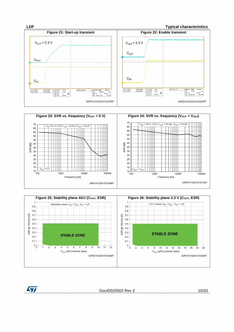
The LDF voltage regulator requires external ceramic capacitors to assure the control loop stability. These capacitors must be selected to meet the requirements of minimum capacitance and equivalent series resistance (see Figure 25: "Stability plane ADJ (COUT, ESR)" and Figure 26: "Stability plane 3.3 V (COUT, ESR)". Input/output capacitors should be located as closer as possible to the relative pins.
6.1.1 Input capacitor
An input capacitor, whose minimum value is 1 μF, must not be located farther than 0.5" from the input pin of the device and returned to a clean analog ground.
6.1.2 Output capacitor
Ceramic capacitors could be used on the output, provided that they must meet the minimum amount of capacitance and E.S.R. (equivalent series resistance) value required. 2.2 μF is suggested as minimum capacitance to guarantee the stability of the regulator. Anyway, other COUT values can be used according to the Figure 25: "Stability plane ADJ (COUT, ESR)" and Figure 26: "Stability plane 3.3 V (COUT, ESR)" showing the allowable ESR range as a function of the output capacitance. The output capacitor must maintain its ESR in the stable region over the full operating temperature range to assure stability. Besides, capacitor tolerance and temperature variation must be taken into account to assure the minimum amount of capacitance.
6.2 Output voltage setting for ADJ version
In the adjustable version, the output voltage can be set from 0.8 V up to the input voltage minus the voltage drop across the pass transistor (dropout voltage), by connecting a resistor divider between the ADJ pin and the output, thus allowing remote voltage sensing.
The resistor divider could be selected by the following equation:
𝑉𝑂𝑈𝑇 = 𝑉𝐴𝐷𝐽(1 + 𝑅1𝑅2⁄ ) 𝑤𝑖𝑡ℎ 𝑉𝐴𝐷𝐽 = 0.8 𝑉(𝑡𝑦𝑝. )
It is recommended to use resistors with values in the range of 10 kΩ to 100 kΩ. Lower values can also be suitable, but current consumption increases.
6.3 Enable pin operation
This pin can be used to turn OFF the regulator when it is pulled down, so to drastically reduce the current consumption. When the enable feature is not used, this pin must be tied to VIN to keep the regulator output in ON state every time. To assure the proper operation, the signal source, used to drive the EN pin, must be able to swing above and below the specified thresholds listed in the electrical characteristics (VEN). The EN pin must not be left floating because it is not internally pulled down/up.
6.4 Power Good
The LDF features an open drain PG pin to sequence either external supplies or loads and to provide fault detection. This pin requires an external resistor (RPG) to pull Power Good high when the output is within the power-good tolerance window. Typical values for this resistor range from 10 kΩ to 100 kΩ.
Typical characteristics LDF
12/33 DocID025502 Rev 2
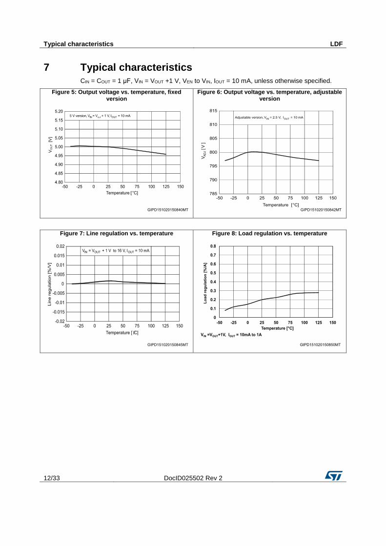
7 Typical characteristics
CIN = COUT = 1 μF, VIN = VOUT +1 V, VEN to VIN, IOUT = 10 mA, unless otherwise specified.
Figure 5: Output voltage vs. temperature, fixed version
Figure 6: Output voltage vs. temperature, adjustable version
Figure 7: Line regulation vs. temperature
Figure 8: Load regulation vs. temperature
LDF Typical characteristics
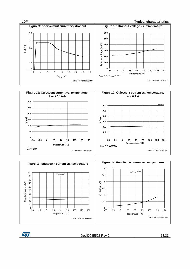
DocID025502 Rev 2 13/33
Figure 9: Short-circuit current vs. dropout
Figure 10: Dropout voltage vs. temperature
Figure 11: Quiescent current vs. temperature,
IOUT = 10 mA
Figure 12: Quiescent current vs. temperature,
IOUT = 1 A
Figure 13: Shutdown current vs. temperature
Figure 14: Enable pin current vs. temperature
Typical characteristics LDF
14/33 DocID025502 Rev 2
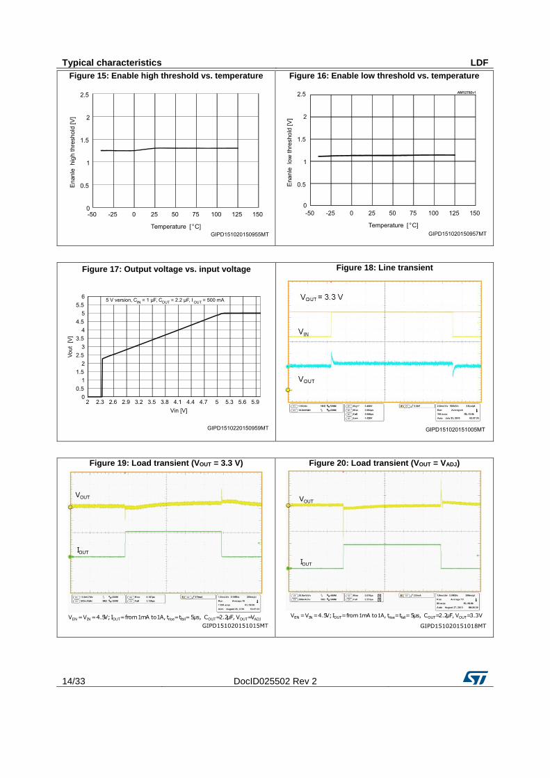
Figure 15: Enable high threshold vs. temperature
Figure 16: Enable low threshold vs. temperature
Figure 17: Output voltage vs. input voltage
Figure 18: Line transient
Figure 19: Load transient (VOUT = 3.3 V)
Figure 20: Load transient (VOUT = VADJ)
LDF Typical characteristics
DocID025502 Rev 2 15/33
Figure 21: Start-up transient
Figure 22: Enable transient
Figure 23: SVR vs. frequency (VOUT = 5 V)
Figure 24: SVR vs. frequency (VOUT = VADJ)
Figure 25: Stability plane ADJ (COUT, ESR)
Figure 26: Stability plane 3.3 V (COUT, ESR)
Package information LDF
16/33 DocID025502 Rev 2
8 Package information
In order to meet environmental requirements, ST offers these devices in different grades of ECOPACK® packages, depending on their level of environmental compliance. ECOPACK® specifications, grade definitions and product status are available at: www.st.com. ECOPACK® is an ST trademark.
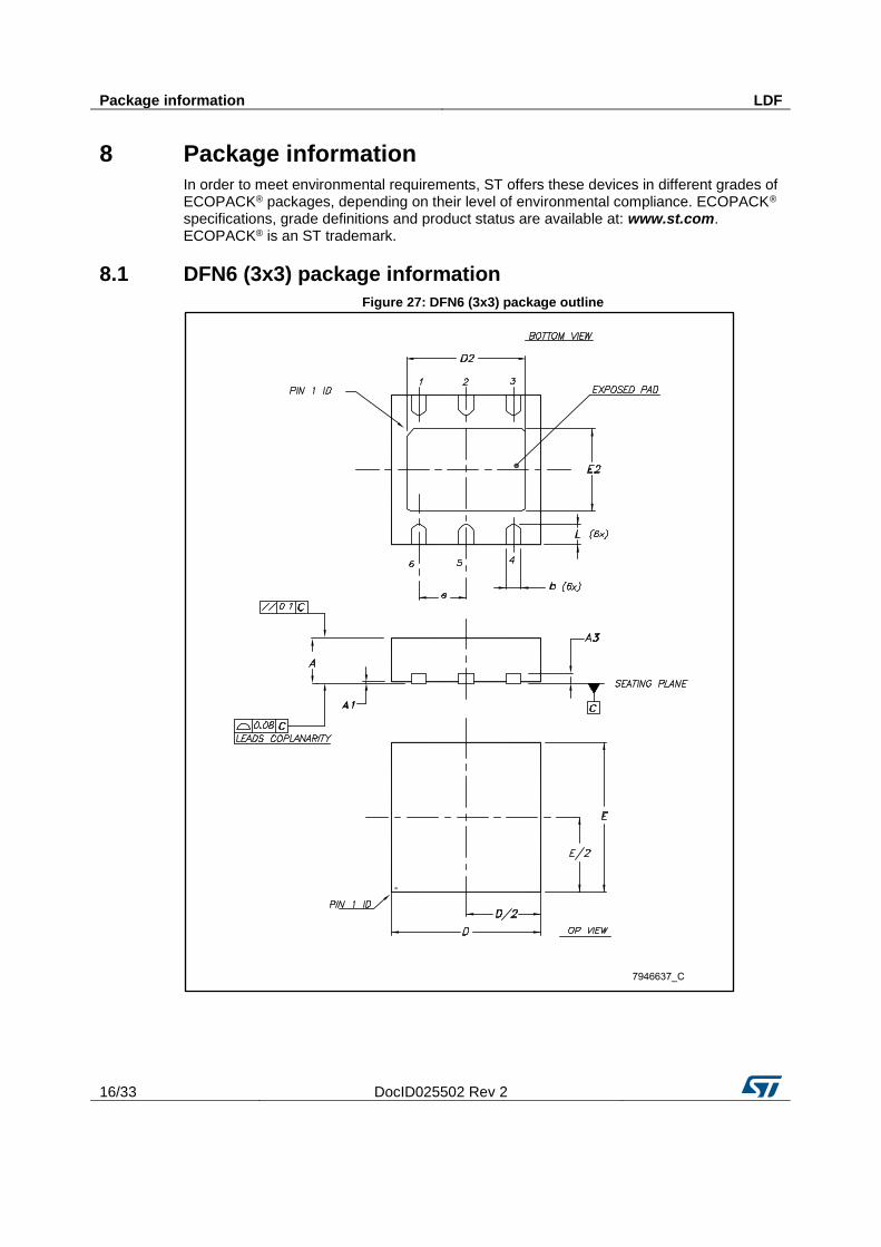
8.1 DFN6 (3x3) package information
Figure 27: DFN6 (3x3) package outline

LDF Package information
DocID025502 Rev 2 17/33
Table 7: DFN6 (3x3) mechanical data
Dim. mm
Min. Typ. Max.
A 0.80
1
A1 0 0.02 0.05
A3
0.20
b 0.23
0.45
D 2.90 3 3.10
D2 2.23
2.50
E 2.90 3 3.10
E2 1.50
1.75
e
0.95
L 0.30 0.40 0.50
Figure 28: DFN6 (3x3) recommended footprint
Package information LDF
18/33 DocID025502 Rev 2
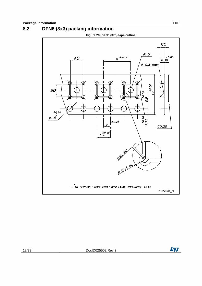
8.2 DFN6 (3x3) packing information
Figure 29: DFN6 (3x3) tape outline
7875978_N
LDF Package information
DocID025502 Rev 2 19/33
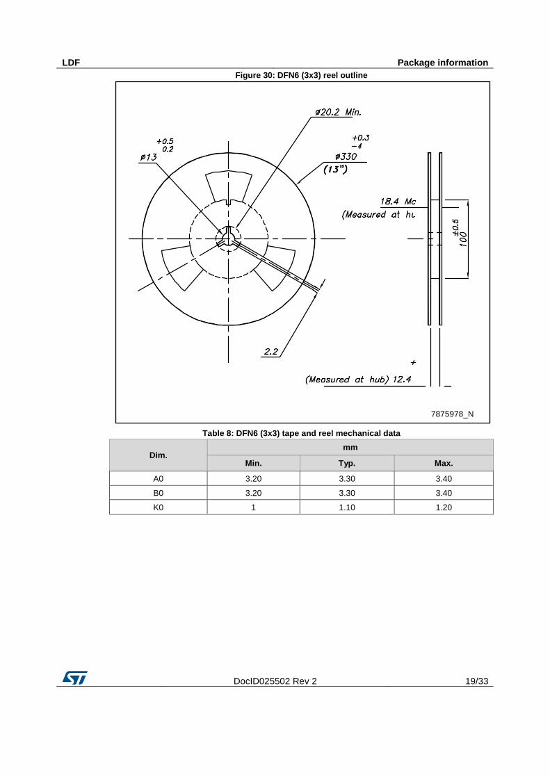
Figure 30: DFN6 (3x3) reel outline
Table 8: DFN6 (3x3) tape and reel mechanical data
Dim. mm
Min. Typ. Max.
A0 3.20 3.30 3.40
B0 3.20 3.30 3.40
K0 1 1.10 1.20
7875978_N
Package information LDF
20/33 DocID025502 Rev 2
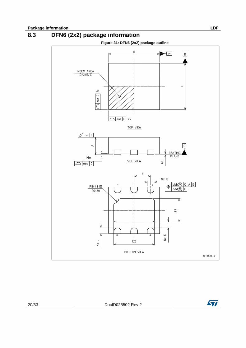
8.3 DFN6 (2x2) package information
Figure 31: DFN6 (2x2) package outline
LDF Package information
DocID025502 Rev 2 21/33
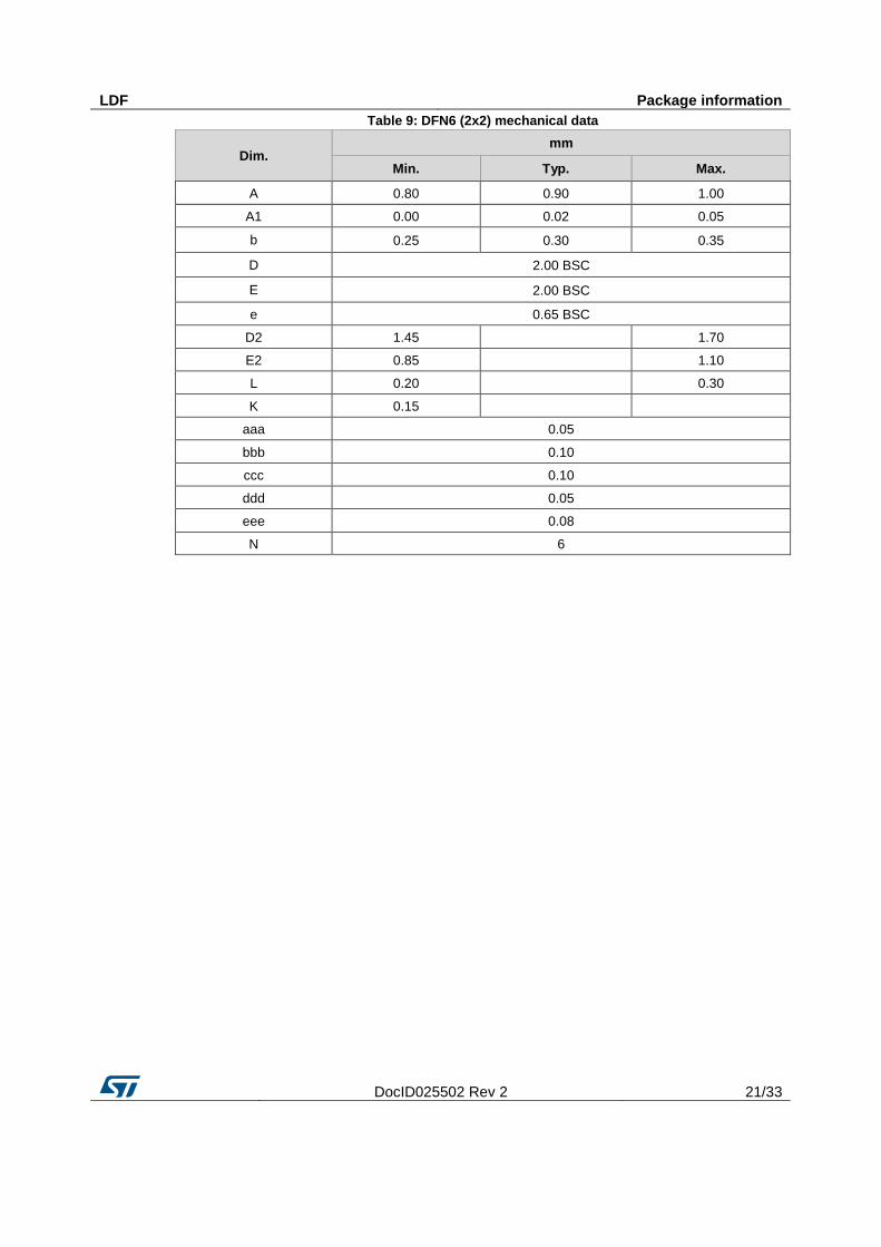
Table 9: DFN6 (2x2) mechanical data
Dim. mm
Min. Typ. Max.
A 0.80 0.90 1.00
A1 0.00 0.02 0.05
b 0.25 0.30 0.35
D 2.00 BSC
E 2.00 BSC
e 0.65 BSC
D2 1.45
1.70
E2 0.85
1.10
L 0.20
0.30
K 0.15
aaa 0.05
bbb 0.10
ccc 0.10
ddd 0.05
eee 0.08
N 6
Package information LDF
22/33 DocID025502 Rev 2
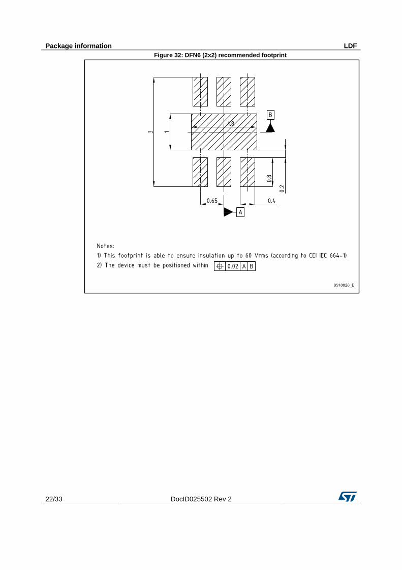
Figure 32: DFN6 (2x2) recommended footprint
LDF Package information
DocID025502 Rev 2 23/33
8.4 DFN6 (2x2) packing information
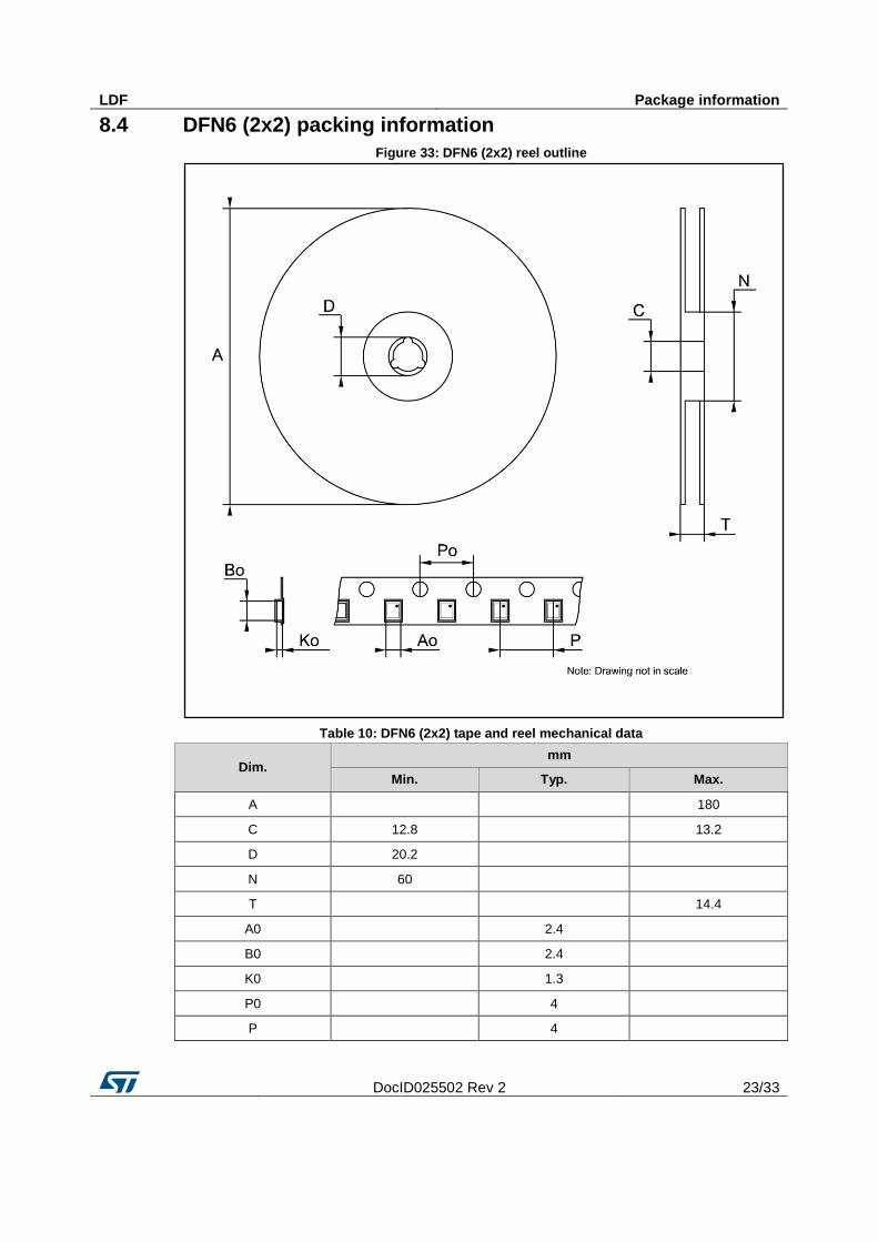
Figure 33: DFN6 (2x2) reel outline
Table 10: DFN6 (2x2) tape and reel mechanical data
Dim. mm
Min. Typ. Max.
A
180
C 12.8
13.2
D 20.2
N 60
T
14.4
A0
2.4
B0
2.4
K0
1.3
P0
4
P
4

Package information LDF
24/33 DocID025502 Rev 2
8.5 PPAK package information
Figure 34: PPAK package outline

LDF Package information
DocID025502 Rev 2 25/33
Table 11: PPAK mechanical data
Dim. mm
Min. Typ. Max.
A 2.2
2.4
A1 0.9
1.1
A2 0.03
0.23
B 0.4
0.6
B2 5.2
5.4
C 0.45
0.6
C2 0.48
0.6
D 6
6.2
D1
5.1
E 6.4
6.6
E1
4.7
e
1.27
G 4.9
5.25
G1 2.38
2.7
H 9.35
10.1
L2
0.8 1
L4 0.6
1
L5 1
L6
2.8
R
0.20
V2 0°
8°
Package information LDF
26/33 DocID025502 Rev 2
8.6 DPAK package information
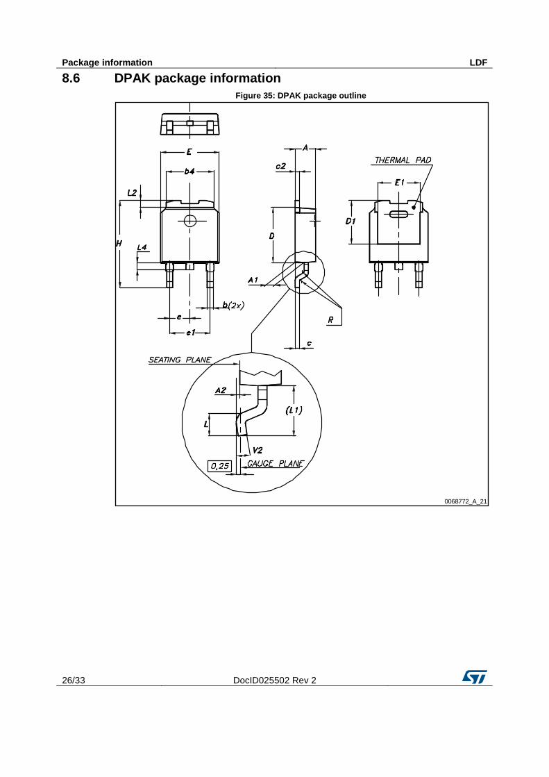
Figure 35: DPAK package outline
0068772_A_21
LDF Package information
DocID025502 Rev 2 27/33
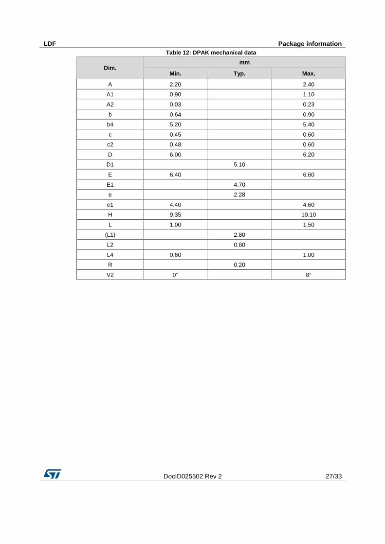
Table 12: DPAK mechanical data
Dim. mm
Min. Typ. Max.
A 2.20
2.40
A1 0.90
1.10
A2 0.03
0.23
b 0.64
0.90
b4 5.20
5.40
c 0.45
0.60
c2 0.48
0.60
D 6.00
6.20
D1
5.10
E 6.40
6.60
E1
4.70
e
2.28
e1 4.40
4.60
H 9.35
10.10
L 1.00
1.50
(L1)
2.80
L2
0.80
L4 0.60
1.00
R
0.20
V2 0°
8°
Package information LDF
28/33 DocID025502 Rev 2
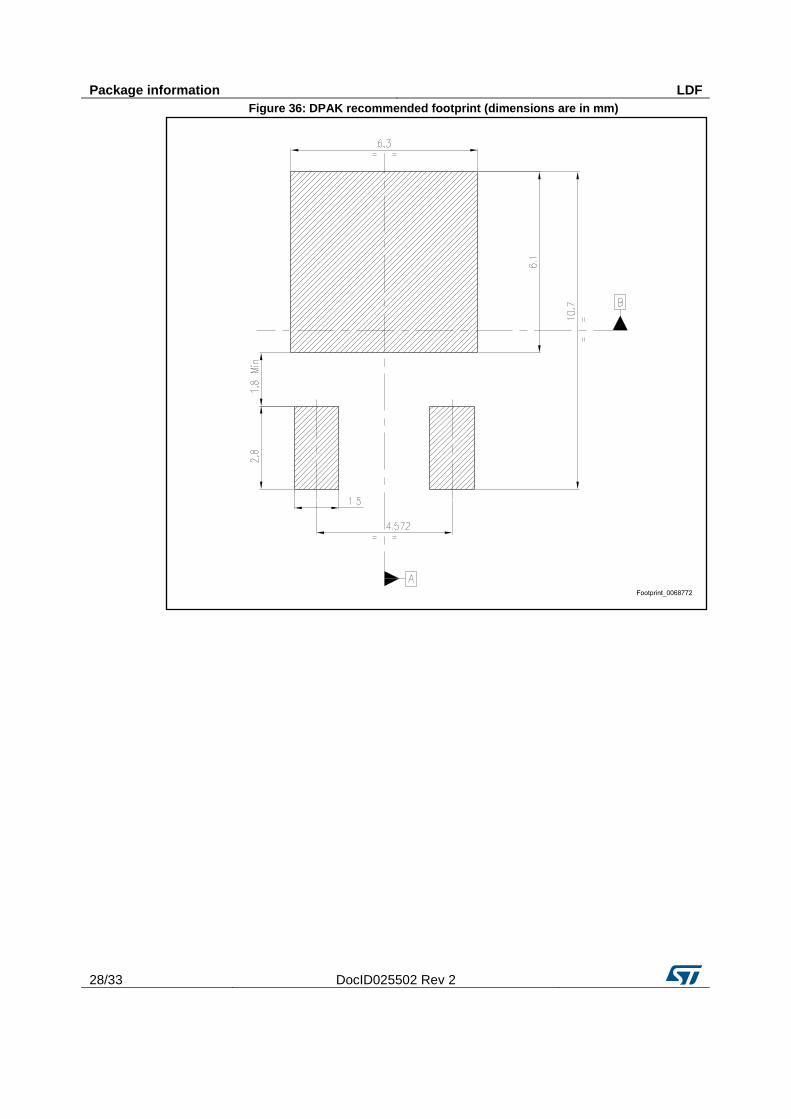
Figure 36: DPAK recommended footprint (dimensions are in mm)
LDF Package information
DocID025502 Rev 2 29/33
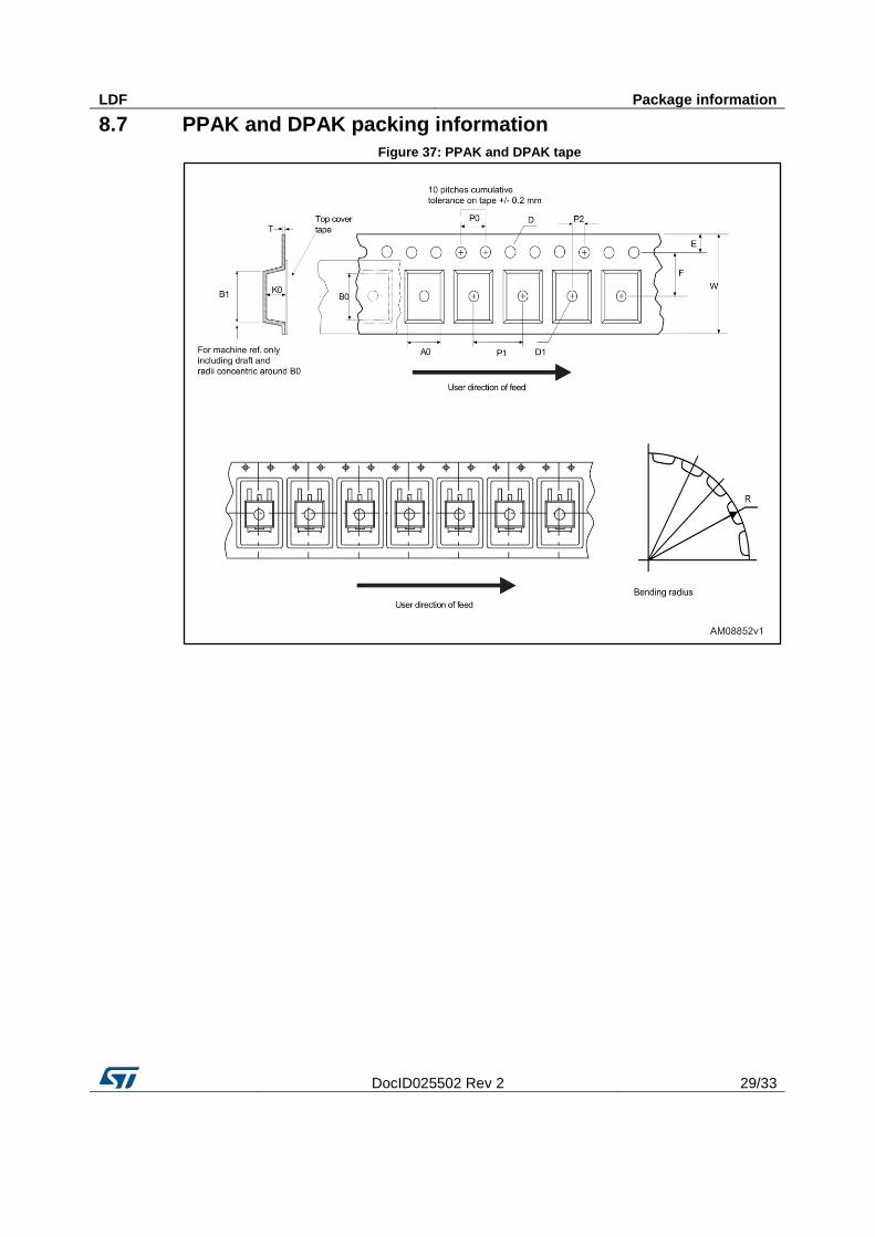
8.7 PPAK and DPAK packing information
Figure 37: PPAK and DPAK tape
Package information LDF
30/33 DocID025502 Rev 2
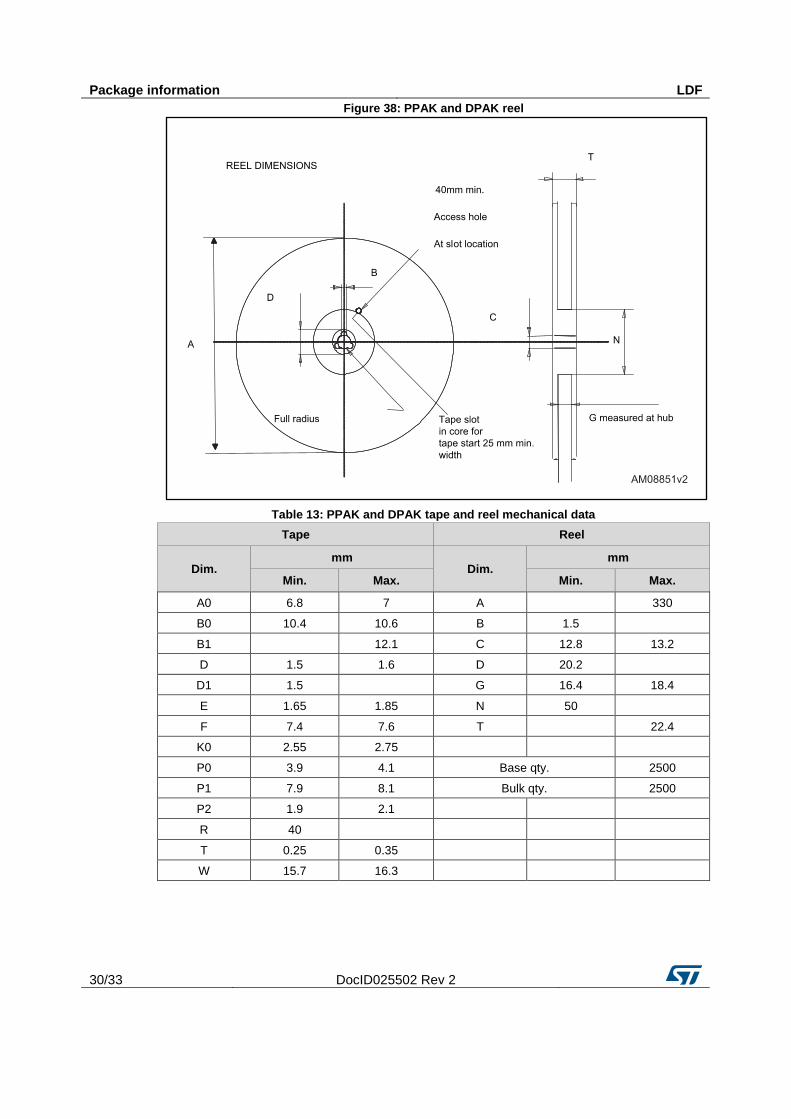
Figure 38: PPAK and DPAK reel
Table 13: PPAK and DPAK tape and reel mechanical data
Tape Reel
Dim. mm
Dim. mm
Min. Max. Min. Max.
A0 6.8 7 A
330
B0 10.4 10.6 B 1.5
B1
12.1 C 12.8 13.2
D 1.5 1.6 D 20.2
D1 1.5
G 16.4 18.4
E 1.65 1.85 N 50
F 7.4 7.6 T
22.4
K0 2.55 2.75
P0 3.9 4.1 Base qty. 2500
P1 7.9 8.1 Bulk qty. 2500
P2 1.9 2.1
R 40
T 0.25 0.35
W 15.7 16.3
LDF Ordering information
DocID025502 Rev 2 31/33
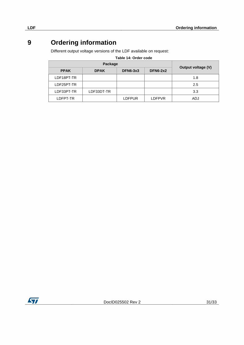
9 Ordering information
Different output voltage versions of the LDF available on request:
Table 14: Order code
Package Output voltage (V)
PPAK DPAK DFN6-3x3 DFN6-2x2
LDF18PT-TR
1.8
LDF25PT-TR
2.5
LDF33PT-TR LDF33DT-TR
3.3
LDFPT-TR
LDFPUR LDFPVR ADJ
Revision history LDF
32/33 DocID025502 Rev 2
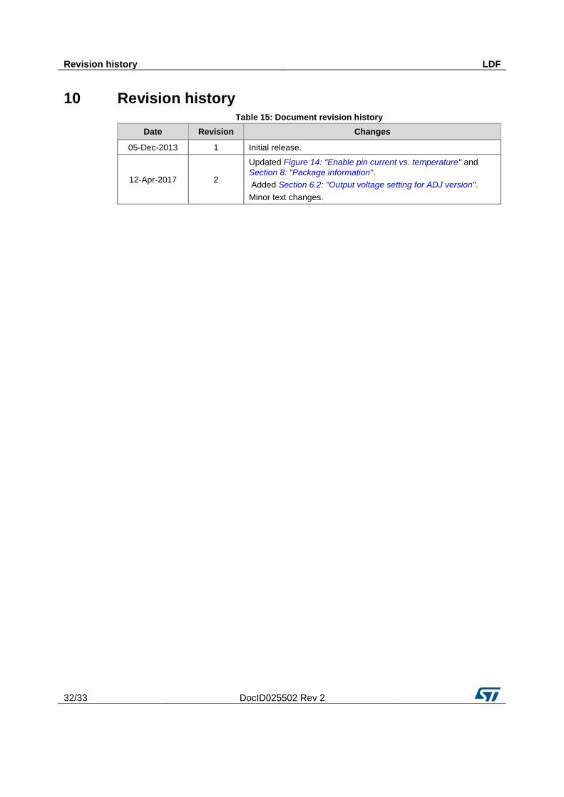
10 Revision history Table 15: Document revision history
Date Revision Changes
05-Dec-2013 1 Initial release.
12-Apr-2017 2
Updated Figure 14: "Enable pin current vs. temperature" and
Section 8: "Package information".
Added Section 6.2: "Output voltage setting for ADJ version".
Minor text changes.
LDF
DocID025502 Rev 2 33/33
IMPORTANT NOTICE – PLEASE READ CAREFULLY
STMicroelectronics NV and its subsidiaries (“ST”) reserve the right to make changes, corrections, enhancements, modifications, and improvements to ST products and/or to this document at any time without notice. Purchasers should obtain the latest relevant information on ST products before placing orders. ST products are sold pursuant to ST’s terms and conditions of sale in place at the time of order acknowledgement.
Purchasers are solely responsible for the choice, selection, and use of ST products and ST assumes no liability for application assistance or the design of Purchasers’ products.
No license, express or implied, to any intellectual property right is granted by ST herein.
Resale of ST products with provisions different from the information set forth herein shall void any warranty granted by ST for such product.
ST and the ST logo are trademarks of ST. All other product or service names are the property of their respective owners.
Information in this document supersedes and replaces information previously supplied in any prior versions of this document.
© 2017 STMicroelectronics – All rights reserved