1 21 August 2015 Electronic and Interconnect Solutions Division Using Tape & Reel for High Volume...
31
1 March 13, 202 2 Electronic and Interconnect Solutions Division Using Tape & Reel for High Volume Flip Chip Delivery: A Manufacturing Analysis Joint Study by: Pat Jones - Delco Electronics Corporation Lisa Bernal Brethour - Surface Mount Taping, Inc. Tom Becker - 3M Presented at MCC/EIA/SEMATECH KGD Industry Workshop September 19, 1997
-
Upload
melina-greene -
Category
Documents
-
view
223 -
download
1
Transcript of 1 21 August 2015 Electronic and Interconnect Solutions Division Using Tape & Reel for High Volume...

1April 19, 2023Electronic and Interconnect Solutions Division
Using Tape & Reel for High Volume Flip Chip Delivery: A Manufacturing Analysis
Joint Study by:
Pat Jones - Delco Electronics Corporation
Lisa Bernal Brethour - Surface Mount Taping, Inc.
Tom Becker - 3M
Presented atMCC/EIA/SEMATECH KGD Industry Workshop
September 19, 1997

2April 19, 2023Electronic and Interconnect Solutions Division
Presentation Outline
• Background
• Test Plan
• Test Procedure
• Material Selection
• Wafer to Tape and Reel Results
• Transportation Test Results
• Bump Shape Analysis
• Spectral Analysis
• Pick and Place Test Results
• Conclusions and Recommendations
3April 19, 2023Electronic and Interconnect Solutions Division
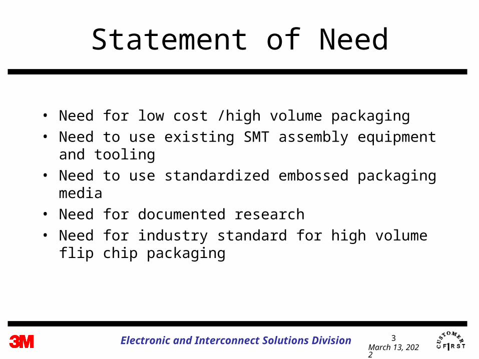
Statement of Need
• Need for low cost /high volume packaging
• Need to use existing SMT assembly equipment and tooling
• Need to use standardized embossed packaging media
• Need for documented research
• Need for industry standard for high volume flip chip packaging

4April 19, 2023Electronic and Interconnect Solutions Division
Objective
• Determine feasibility of using standard embossed tape and reel packaging for flip chip ICs bumps down
• Determine functional “range of sizes” of flip chips in standard pockets
• Provide design model for sizing embossed pockets to flip chips
• Provide research to the semiconductor industry to assist in standardization
5April 19, 2023Electronic and Interconnect Solutions Division
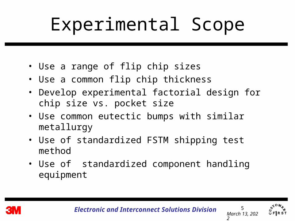
Experimental Scope
• Use a range of flip chip sizes
• Use a common flip chip thickness
• Develop experimental factorial design for chip size vs. pocket size
• Use common eutectic bumps with similar metallurgy
• Use of standardized FSTM shipping test method
• Use of standardized component handling equipment

6April 19, 2023Electronic and Interconnect Solutions Division
3M Motorola Delco
Tape Sizing Factorial and Rotation Analysis Tape Design and Manufacture Tape Re-design and Manufacture
Wafer Bumping Wafer Processing Flip Chip Inspection Transfer to Gel Pak Transfer to Tape & Reel Wafer to Tape Analysis Sample Shipment
Wafer Fab Wafer Bumping Wafers to Motorola Transportation Test Bump Inspection Bump Measurement Spectral Analysis Pick and Place Experiment
All : Analysis & Report Generation
Joint Division of Responsibilities

7April 19, 2023Electronic and Interconnect Solutions Division
Process Flow
Delco Electronics Wafers
MotorolaBump
Delco Electronics
Bump
MotorolaWafer to Tape
Delco ElectronicsTest/Assembly
3M Tape & Reel
Motorola, SPSWafers

8April 19, 2023Electronic and Interconnect Solutions Division
Flip Chip Description
*Bump Metallurgy: Eutectic Sn/Pb 60/40 or 63/37
Name Size Chip Thickness Number of Bump Pattern(mm) (mm) Bumps
Small FDIZ 1.3 x 1.3 0.81 6 Array
Mid-Size MSFB-1UP 5.8 x 5.8 0.69 96 PerimeterFB250 6.35 x 6.35 0.72 48 3 Row ArrayMFDS 4.34 x 5.63 0.76 40 Array
Large MSFB-4UP 11.17 x 12.6 0.72 384 ArrayTC10 6.6 x 9.47 0.72 150 Perimeter

9April 19, 2023Electronic and Interconnect Solutions Division
Flip Chip Photos
8 mm Tape
24 mm Tape 12 & 16 mm Tape
MSFB,4-UP
MFDS
MSFBFDIZ
Photos to scale

10April 19, 2023Electronic and Interconnect Solutions Division
Embossed Carrier Description
• 3M™ Conductive Polycarbonate Carrier 3000BD
• 3M™ Conductive PSA Cover Tape 2666
• Precision Flat-bottom Pockets
• All pockets (except TC10) are “worst-case” for bump contact with carrier
• Bevel Edge with Raised Cross-bar pocket design
Bare Die
< 3.0 deg. Draft AngleInside Corner
Flat-bottomPocket
Bevel < 35 deg..
Bevel at50% of Ko
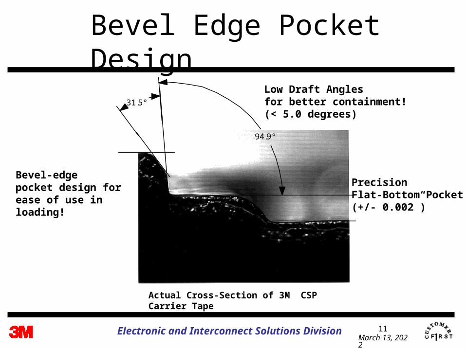
11April 19, 2023Electronic and Interconnect Solutions Division
Bevel Edge Pocket Design
Bevel-edgepocket design for ease of use in loading!
Low Draft Anglesfor better containment!(< 5.0 degrees)
PrecisionFlat-Bottom Pocket(+/- 0.002”)
Actual Cross-Section of 3M CSP Carrier Tape
31.5°
94.9°
12April 19, 2023Electronic and Interconnect Solutions Division
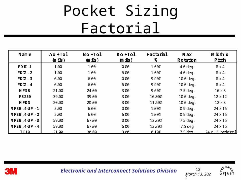
Pocket Sizing Factorial
Name Ao +Tol Bo +Tol Ko +Tol Factorial Max Width x (mils) (mils) (mils) % Rotation Pitch
FDIZ -1 1.00 1.00 0.00 1.00% 4.0 deg. 8 x 4
FDIZ - 2 1.00 1.00 6.00 1.00% 4.0 deg. 8 x 4
FDIZ - 3 6.00 6.00 0.00 9.90% 10.0 deg. 8 x 4
FDIZ - 4 6.00 6.00 6.00 9.90% 10.0 deg. 8 x 4
MFSB 21.00 24.00 3.00 9.60% 7.5 deg. 16 x 8
FB250 39.00 39.00 3.00 16.00% 10.0 deg. 12 x 12
MFDS 20.00 20.00 3.00 11.60% 10.0 deg. 12 x 8
MFSB, 4-UP - 1 5.00 6.00 0.00 1.00% 0.9 deg. 24 x 16
MFSB, 4-UP - 2 5.00 6.00 6.00 1.00% 0.9 deg. 24 x 16
MFSB, 4-UP - 3 59.00 67.00 0.00 13.30% 7.5 deg. 24 x 16
MFSB, 4-UP - 4 59.00 67.00 6.00 13.30% 7.5 deg 24 x 16
TC10 21.00 30.00 3.00 8.10% 7.5 deg. 24 x 12 pedestal

13April 19, 2023Electronic and Interconnect Solutions Division
Wafer-to-Tape Process
• 100% visual inspection performed prior to pick manually inked damaged chips
• Bumps inspected to Delco Electronics Workmanship Standards
• Manually placed control dice in Gel-Pak®, bumps up
• Generated vibration samples versus control in tape and reel
Gel-Pak® is a product of Vichem Corporation

14April 19, 2023Electronic and Interconnect Solutions Division
Wafer-to-Tape Equipment
15April 19, 2023Electronic and Interconnect Solutions Division
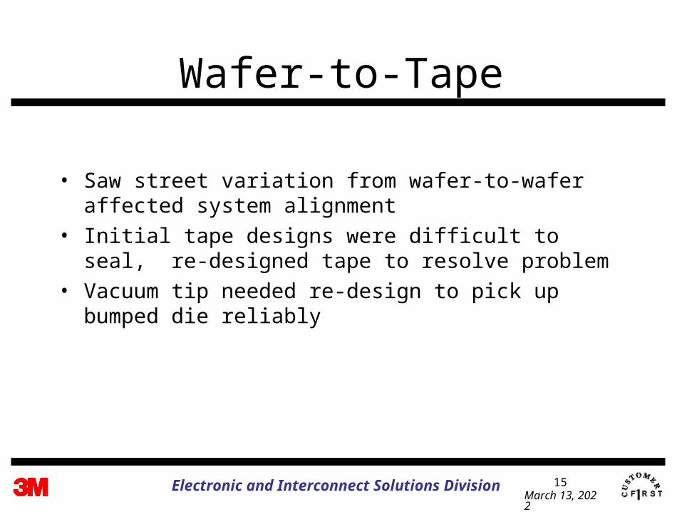
Wafer-to-Tape
• Saw street variation from wafer-to-wafer affected system alignment
• Initial tape designs were difficult to seal, re-designed tape to resolve problem
• Vacuum tip needed re-design to pick up bumped die reliably

16April 19, 2023Electronic and Interconnect Solutions Division
Wafer-to-Tape Results
Flip-Chip Misplaced Dice UPHFDIZ - Tape 1 0.80% 1200FDIZ - Tape 2 13.20% 1200FDIZ - Tape 3 0.00% 1560FDIZ - Tape 4 1.20% 1560MFDS 0.04% 2760FB250 0.94% 3000MSFB1-UP 0.00% 2520MSFB4-UP Tape 1 2.60%MSFB4-UP Tape 2 1.30%MSFB4-UP Tape 3 2.70%MSFB4-UP Tape 4 0.00%TC10 0.06% 2220

17April 19, 2023Electronic and Interconnect Solutions Division
Packaging and Shipping Method
• Partially filled 13” reels
• Anti-static bags
• Placed in primary shipping container (pizza box) with anti-static bubble wrap
• Placed in secondary shipping container with anti-static bubble wrap
• Shipped UPS Red
- Tempe, AZ to Kokomo, IN
18April 19, 2023Electronic and Interconnect Solutions Division
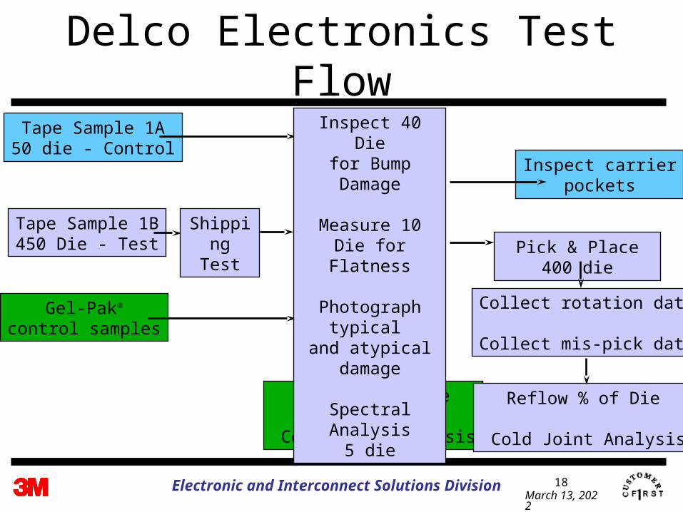
Delco Electronics Test Flow
Tape Sample 1A50 die - Control
Tape Sample 1B450 Die - Test
Gel-Pak®
control samples
Inspect carrierpockets
Pick & Place 400 die
Collect rotation data
Collect mis-pick data
Reflow % of Die
Cold Joint Analysis
Inspect 40 Diefor Bump Damage
Measure 10 Die forFlatness
Photograph typical and atypical
damage
Spectral Analysis5 die
Reflow % of Die
Cold Joint Analysis
Shipping Test

19April 19, 2023Electronic and Interconnect Solutions Division
Shipping Test
• Federal Standard Test Method 101C:
• Vibration Method 5019.1
– Vibrate on 3 sides - one hour each
– 0.5” unrestrained vertical movement
• Drop Test Method 5007.1
– Level B, procedures b, c and f
– 27” drop height

20April 19, 2023Electronic and Interconnect Solutions Division
FDIZ Bump Photos
Control Gel-Pak® Control Tape & Reel Test Sample
SEM Photos

21April 19, 2023Electronic and Interconnect Solutions Division
MSFB Bump Photos
Control Gel-Pak® Control Tape & Reel Test Sample
SEM Photos
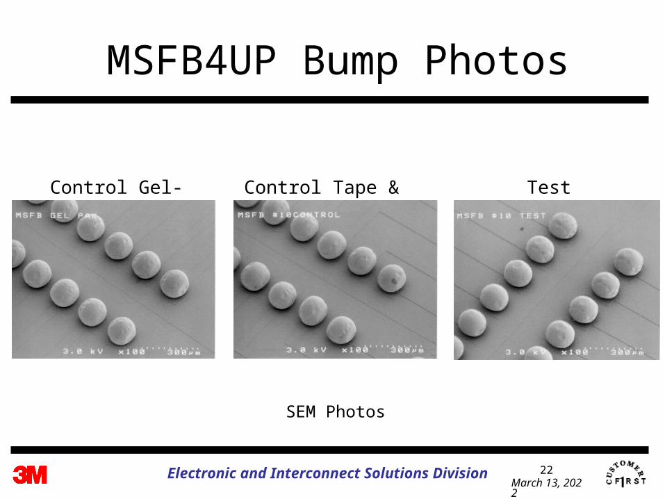
22April 19, 2023Electronic and Interconnect Solutions Division
MSFB4UP Bump Photos
Control Gel-Pak® Control Tape & Reel Test Sample
SEM Photos

23April 19, 2023Electronic and Interconnect Solutions Division
FB250 Bump Photos
Control Gel-Pak® Control Tape & Reel Test Sample
SEM Photos

24April 19, 2023Electronic and Interconnect Solutions Division
Bump Height Statistical Analysis
• Using computerized optical measuring system
– Repeatable to 2.5 um
– Analysis of mid-size FB250 bumps
• Analyzed bump heights and flatness
• Average and sigma

25April 19, 2023Electronic and Interconnect Solutions Division
Bump Heights - Average
XBAR: Bump Heights25 devices
48 bumps/device
0.06
0.065
0.07
0.075
0.08
0.085
0.09
0.095
0.1
1 3 5 7 9 11
13
15
17
19
21
23
25
CONTROL: Gel Pack
EMBOSSED: No Vibration orDrop
TEST- Vibrated/Drop Tested

26April 19, 2023Electronic and Interconnect Solutions Division
Bump Heights - Sigma
SIGMA: Bump Heights25 devices
48 bumps/device
0.006
0.008
0.01
0.012
0.014
0.016
0.018
1 3 5 7 9 11
13
15
17
19
21
23
25
EMBOSSED: No Vibration orDrop
CONTROL: Gel Pack
TEST- Vibrated/Drop Tested
27April 19, 2023Electronic and Interconnect Solutions Division
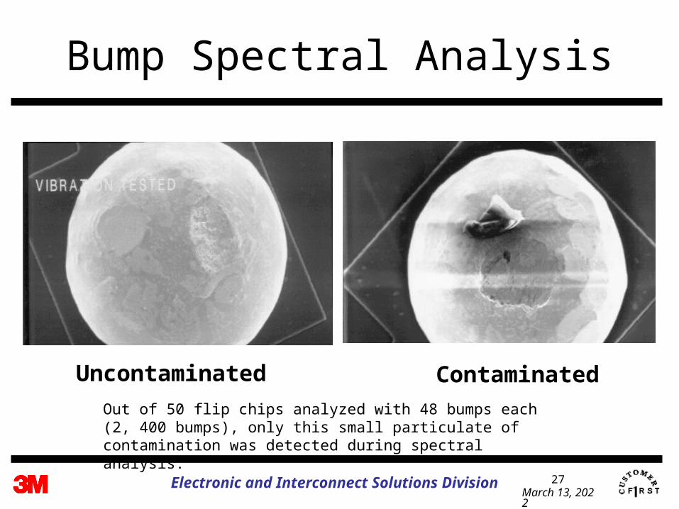
Bump Spectral Analysis
Uncontaminated Contaminated
Out of 50 flip chips analyzed with 48 bumps each (2, 400 bumps), only this small particulate of contamination was detected during spectral analysis.
28April 19, 2023Electronic and Interconnect Solutions Division
Substrate Assembly Process
• SMD equipment with standard feeders (blind pick!)
• Data collection
– Rotation of flip chips in pockets
– Mis-pick information
• Reflow on test PCBs
• Comparison of modules with control vs. tested flip chips

29April 19, 2023Electronic and Interconnect Solutions Division
Pick and Place Test ResultsFlip-Chip Pick & Place #1 Pick & Place #2FDIZ - Tape 1 6.6% 0.0%FDIZ - Tape 2 10.0% 0.0%FDIZ - Tape 3 30.0% 0.0%FDIZ - Tape 4 13.0% 0.0%MFDS N/A 3.5%MSFB1-UP 0.0% N/AMSFB4-UP Tape 1 0.0% 5.0%MSFB4-UP Tape 2 0.0% 10.0%MSFB4-UP Tape 3 25.0% 5.0%MSFB4-UP Tape 4 0.0% 5.0%TC10 N/A 6.0%
*P&P #1 vacuum chuck was not optimized for small die and had difficulty picking up the FDIZ components.
*P&P #2 vision system was not optimized for large components and had difficulty “seeing” the large components.

30April 19, 2023Electronic and Interconnect Solutions Division
Conclusions and Recommendations
• Use of standardized embossed tape & reel solves high volume/low cost transportation needs
• Must limit die movement to < 10 degrees to prevent die damage
• Carrier should be cleaned prior to use
• Existing SMT placement equipment is capable of blind picking flip chips from carrier tapes
31April 19, 2023Electronic and Interconnect Solutions Division
Important Notice
Important NoticeBefore using this product, you must evaluate it and determine if it is suitable for your intended application. You assume all risks and liability associated with such use.
Warranty; Limited Remedy; Limited Liability3M’s product warranty is stated in its Product Literature available upon request. 3M MAKES NO OTHER WARRANTIES INCLUDING, BUT NOT LIMITED TO, ANY IMPLIED WARRANTY OF MERCHANTABILITY OR FITNESS FOR A PARTICULAR PURPOSE. If this product is defective within the warranty period stated above, your exclusive remedy shall be, at 3M’s option, to replace or repair the 3M product or refund the purchase price of the 3M product. Except where prohibited by law, 3M will not be liable for any loss or damage arising from this 3M product, whether direct, indirect, special, incidental or consequential regardless of the legal theory asserted.
3M is a trademark of 3M Company.