.1 1999 ©UCB CS 161Computer Architecture Chapter 5 Instructor: L.N. Bhuyan bhuyan LECTURE 10.
21
.1 1999 ©UCB CS 161Computer Architecture Chapter 5 Instructor: L.N. Bhuyan www.cs.ucr.edu/~bhuyan LECTURE 10
-
date post
21-Dec-2015 -
Category
Documents
-
view
219 -
download
0
Transcript of .1 1999 ©UCB CS 161Computer Architecture Chapter 5 Instructor: L.N. Bhuyan bhuyan LECTURE 10.

.1 1999 ©UCB
CS 161Computer Architecture
Chapter 5
Instructor: L.N. Bhuyanwww.cs.ucr.edu/~bhuyan
LECTURE 10

.2 1999 ©UCB
Compose Datapath: R-form + Load/Store
Registers
ReadRegister 1 Read
data 1ALURead
data 2
ReadRegister 2
WriteRegister
WriteData
Instr-uction
Zero
ALU control
4
RegWrite
Address
Readdata
WriteData
SignExtend 32
16
Dmem
MemRead
MemWrite
1Mux0
MemTo-Reg0=R-form1=L/SM
ux
ALUSrc0 = R-format1 = Load/Store
Add muxes

.3 1999 ©UCB
Compose Datapath: … + Imem + PC
Registers
ReadReg1
Readdata1 A
LURead
data2
ReadReg2
WriteReg
WriteData
Zero
ALU control
4
RegWrite
Address
Readdata
WriteData
SignExtend 32
16
Dmem
MemRead
MemWrite
Mux
MemTo-Reg
Mux
ALUSrc
Read Addr
Instruc-tion
Imem
“4”
PC
add

.4 1999 ©UCB
Compose Datapath: … + Branch
Registers
ReadReg1
Readdata1
ALURead
data2
ReadReg2
WriteReg
WriteData
Zero
ALUcon
RegWrite
Address
Readdata
WriteData
SignExtend 32
16
Dmem
MemRead
MemWrite
Mux
MemTo-Reg
Mux
ALUSrc
Read Addr
Instruc-tion
Imem
“4”
PC
add
add <<
2
Mux
PCSrc
“Left Shift 2”module
What about jump?

.5 1999 ©UCB
Recap: Single-Cycle Datapath
Registers
ReadReg1
Readdata1
ALURead
data2
ReadReg2
WriteReg
WriteData
Zero
ALU con
RegWrite
Address
Readdata
WriteData
SignExtend 32
16
Dmem
MemRead
MemWrite
Mux
MemTo-Reg
Mux
ALUSrc
Read Addr
Instruc-tion
Imem
“4”
PC
add
add <<
2
Mux
PCSrc
4
Supports allMIPS-lite instrns?

.6 1999 ©UCB
Datapath: Miscellaneous Details°Wrinkle: destination registers may differ across instruction formats:
• R-format: [rd] <- [rs] op [rt]add $t0,$s0,$s1, For this
instn, bits 11-15 is destination (t0), which should be connected to the write reg.
• I-format: [rt] <- mem[[rs] + imm16]lw $t0,24($s3), For this
instn, bits 16-20 should go to the write port. Bits 0-15 go to the ALU as address.
• Connection to the write port changes!
°Solution? mux to the rescue!

.7 1999 ©UCB
Datapath (add RegDst Mux)
Regs
ReadReg1
Readdata1
ALURead
data2
ReadReg2
WriteReg
WriteData
Zero
ALU-con
RegWrite
Address
Readdata
WriteData
SignExtend
Dmem
MemRead
MemWrite
Mux
MemTo-Reg
Mux
Read Addr
Instruc-tion
Imem
4
PC
add
add <<
2
Mux
PCSrc
ALU-src
Mux
25:21
20:16
15:11
RegDst
15:0
31:0
.8 1999 ©UCB
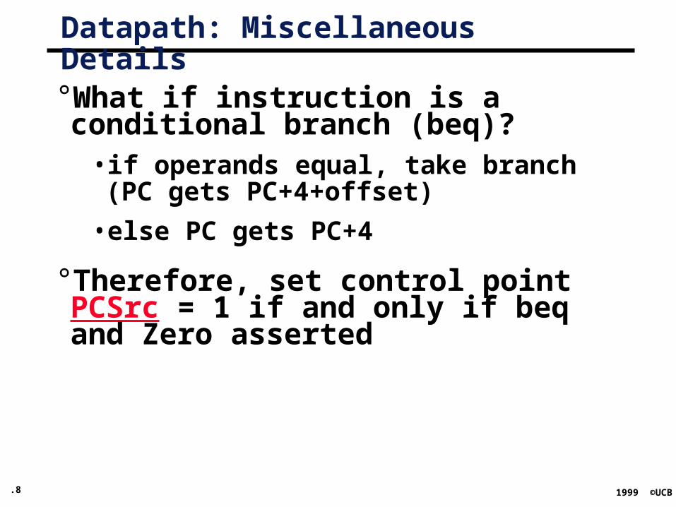
Datapath: Miscellaneous Details°What if instruction is a conditional branch (beq)?
• if operands equal, take branch (PC gets PC+4+offset)
• else PC gets PC+4
°Therefore, set control point PCSrc = 1 if and only if beq and Zero asserted

.9 1999 ©UCB
Datapath (add Branch control point)
Regs
ReadReg1
Readdata1
ALURead
data2
ReadReg2
WriteReg
WriteData
Zero
ALU-con
RegWrite
Address
Readdata
WriteData
SignExtend
Dmem
MemRead
MemWrite
Mux
MemTo-Reg
Mux
Read Addr
Instruc-tion
Imem
4
PC
add
add <<
2
Mux
ALU-src
Mux
25:21
20:16
15:11
RegDst
15:0
31:0
Branch
PCSrc

.10 1999 ©UCB
Adding Control°CPU = Datapath + Control
°Single-Cycle Design:• Instruction takes exactly one clock cycle
• Datapath units used only once per cycle
• Writable state updated at end of cycle
°What must be “controlled”?• Multiplexors (Muxes)
• Writable state elements: Register File, Data Memory (Dmem)
- what about PC? Imem?
• ALU (which operation?)

.11 1999 ©UCB
Processor = Datapath + Control° Single-Cycle Design: everything happens in
one clock cycle
until next falling edge of clock, processor just one big combinational circuit!!!
control is just a combinational circuit(output, just function of inputs)
° outputs? control points in datapath
° inputs? the current instruction! (opcode, funct control everything)

.12 1999 ©UCB
Defining Control
ControlLogic
op rs rt rd shamt funct
R-formatinstruction
To datapath
6 6

.13 1999 ©UCB
Defining Control° Note that funct field only present in R-format instruction - funct controls ALU only
° To simplify control, define Main, ALU control separately – using multiple levels will also increase speed – important optimization technique
° ALUop inputs will be defined
ControlLogic
MainControl
ALUcontrol
op
funct
op
funct
ALU-con
ALUop

.14 1999 ©UCB
Defining ALU Control
ALUcon
ALU
Zero
Result
ALUcon ALU function Instruction(s) supported
0000 AND R-format (and) 0001 OR R-format (or) 0010 add R-format (add), lw, sw 0110 subtract R-format (sub), beq 0111 set on less than R-format (slt) 1100 NOR R-format (nor)
A
B

.15 1999 ©UCB
Defining ALU Control
Instruction Desired opcode ALU Action ALUOp funct ALUcon
lw add 00 xxxxxx 0010sw add 00 xxxxxx 0010beq subtract 01 xxxxxx 0110R-type add 10 100000 (add) 0010R-type subtract 10 100010 (sub) 0110R-type logical AND 10 100100 (and) 0000R-type logical OR 10 100101 (or) 0001R-type set on less 10 101010 (slt) 0111
ALUOp Funct Fielda1 a2 f5 f4 f3 f2 f1 f0 ALUcon
0 0 x x x x x x 0010x 1 x x x x x x 01101 x x x 0 0 0 0 00101 x x x 0 0 1 0 01101 x x x 0 1 0 0 00001 x x x 0 1 0 1 00011 x x x 1 0 1 0 0111
Don’t Cares

.16 1999 ©UCB
Deriving ALUcon outputs
From the truth table, output signals can be easily derived because of don’t cares.
•Operation2 (msb) = ALUOp0 OR (ALUOp1 AND F1)
•Operation1 = ALUOp1 NOR F2
•Operation0 (lsb) = ALUOp1 AND (F3 OR F0)
ALUOp is supplied by the main control unit (to be designed) and F0-F5 are the lsbs of the instruction.
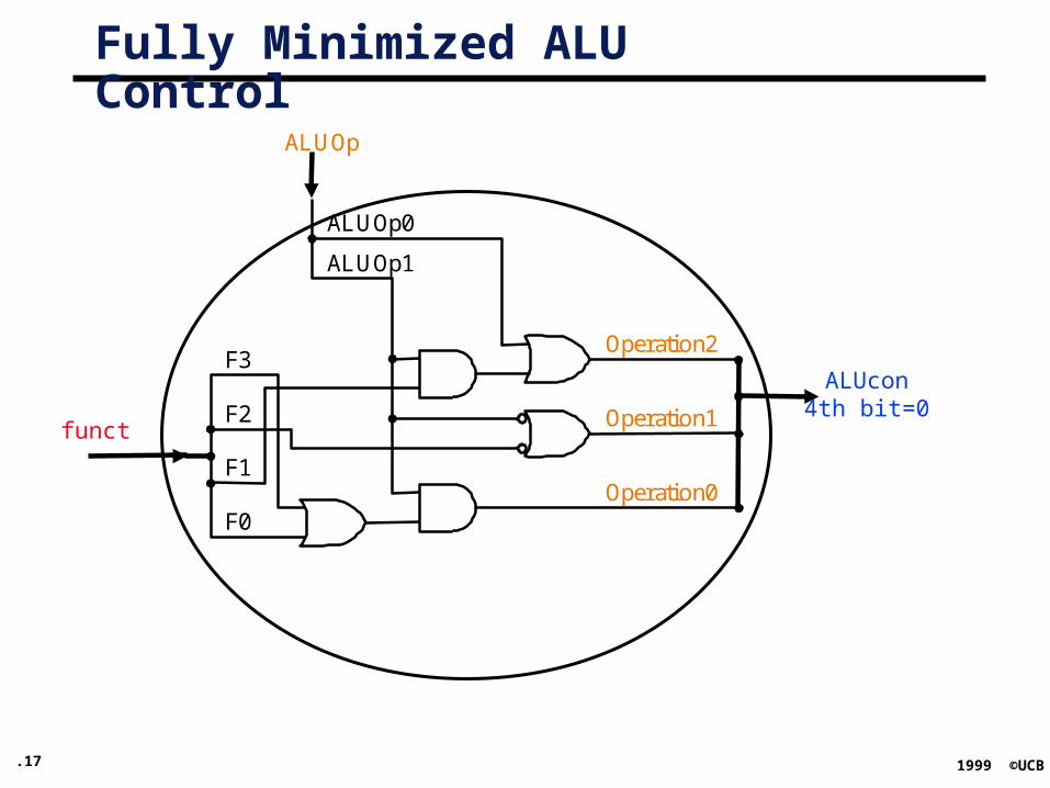
.17 1999 ©UCB
Fully Minimized ALU Control
Operation2
Operation1
Operation0
ALUOp1
F3
F2
F1
F0
ALUOp0
ALUOp
ALUcon4th bit=0
funct

.18 1999 ©UCB
Datapath + ALU Control
Registers
ReadReg1
Readdata1
ALURead
data2
ReadReg2
WriteReg
WriteData
Zero
ALU-con
RegWrite
Address
Readdata
WriteData
SignExtend
Dmem
MemRead
MemWrite
Mux
MemTo-Reg
Mux
Read Addr
Instruc-tion
Imem
“4”
PC
add
add <<
2
Mux
PCSrc
ALU Control
Instr[5:0]ALUOp
ALU-src

.19 1999 ©UCB
Implementing Main Control
Main Control
RegDst
Branch
MemRead
MemtoReg
ALUop
MemWrite
ALUSrc
RegWrite
op
2
Main Control has one 6-bit input, 9 outputs (7 are 1-bit, ALUOp is 2 bits)
To build Main Control as sum-of-products:
(1) Construct a minterm for each different instruction (or R-type); each minterm corresponds to a single instruction (or all of the R-type instructions), e.g., MR-format, Mlw
(2) Determine each main control output by forming the logical OR of relevant minterms (instructions), e.g., RegWrite: MR-format OR Mlw

.20 1999 ©UCB
Single-Cycle MIPS-lite CPU
Regs
ReadReg1
Readdata1
ALURead
data2
ReadReg2
WriteReg
WriteData
Zero
ALU-con
RegWrite
Address
Readdata
WriteData
SignExtend
Dmem
MemRead
MemWrite
Mux
MemTo-Reg
Mux
Read Addr
Instruc-tion
Imem
4
PC
add
add <<
2
Mux
ALU Control
5:0ALUOp
ALU-src
Mux
25:21
20:16
15:11
RegDst
15:0
31:0
Branch
Main Control
op=[31:26]
PCSrc

.21 1999 ©UCB
Adding Jal instrn to datapath1. Jal consists of jump and link for
function calls – jump to the function address (j target) already implemented in Fig. 5.29
2. Place PC+4 (return address) in $ra. So (a) extend the mux at reg input to include 31 ($ra) as another input and (b) expand the mux at write data input to have PC+4 as another input. DRAW on Fig. 5.29.