070823 ISPC-18 School (13) · ISPC-18 Summer School Kyoto, Japan Background As integrated circuit...
45
Plasma Etching August 24, 2007 Department of Aeronautics and Astronautics, Department of Aeronautics and Astronautics, Graduate School of Engineering, Kyoto University, Graduate School of Engineering, Kyoto University, Yoshida Yoshida- Honmachi, Sakyo Honmachi, Sakyo- ku, Kyoto 606 ku, Kyoto 606- 8501, Japan 8501, Japan E-mail: [email protected] Kouichi Ono Kouichi Ono ISPC-18 Summer School Kyoto, Japan Background As integrated circuit device dimensions continue to be scaled down to <0.1 m, strict requirements are being imposed on plasma etching technology. Especially, the precise or nanometer-scale control is indispensable for etched profiles and critical dimensions, together with higher selectivity, higher microscopic uniformity, and less damage. Moreover, new materials such as metals and low- and high-k* dielectrics are being employed for <0.1 m devices, and so the etching of such new materials are also required in integrating them into device fabrication. *k : dielectric constant This lecture presents the current status of plasma etching tech- nology based on the physical and chemical mechanisms underlying the processing, along with the future prospect towards nano-scale processes.
Transcript of 070823 ISPC-18 School (13) · ISPC-18 Summer School Kyoto, Japan Background As integrated circuit...

Plasma Etching
August 24, 2007
Department of Aeronautics and Astronautics, Department of Aeronautics and Astronautics, Graduate School of Engineering, Kyoto University,Graduate School of Engineering, Kyoto University,
YoshidaYoshida--Honmachi, SakyoHonmachi, Sakyo--ku, Kyoto 606ku, Kyoto 606--8501, Japan8501, JapanE-mail: [email protected]
Kouichi OnoKouichi Ono
ISPC-18 Summer SchoolKyoto, Japan
Background�As integrated circuit device dimensions continue to be scaled down to <0.1 �m, strict requirements are being imposed on plasma etching technology.
�Especially, the precise or nanometer-scale control is indispensable for etched profiles and critical dimensions, together with higher selectivity, higher microscopic uniformity, and less damage.
�Moreover, new materials such as metals and low- and high-k*dielectrics are being employed for <0.1 �m devices, and so the etching of such new materials are also required in integrating them into device fabrication. *k : dielectric constant
�This lecture presents the current status of plasma etching tech-nology based on the physical and chemical mechanisms underlying the processing, along with the future prospect towards nano-scale processes.
辻野貴志
タイプライターテキスト
Copyright remains with the author(s).

Outline
1. Introduction1. Introduction�ULSI devices �Requirements for plasma etching technology
2. Fundamentals of Plasma Etching Technology�Etching characteristics �Core technology of Plasma Etching
3. Role of Plasma in Plasma Etching�Gas-phase reactions �Ion acceleration through the sheath
4. Surface Reaction Processes in Plasma Etching�Surface reactions �Ion and neutral transport in microstructures�Feature profile evolution �Microscopic uniformity �Charging
5. Current Issues of Plasma Etching Technology�Current issues �Poly-Si gate etch �High-k gate etch�Metal etch �Deep RIE
6. Summary�Future prospects
1. Introduction� Si-ULSI Devices� Requirements for Plasma Etching

Logic Technology Families
http://www.tsmc.com
Si- ULSI Devices
http://www.intel.com/research/silicon
Si- ULSI Devices (continued)
http://www.intel.com/research/silicon
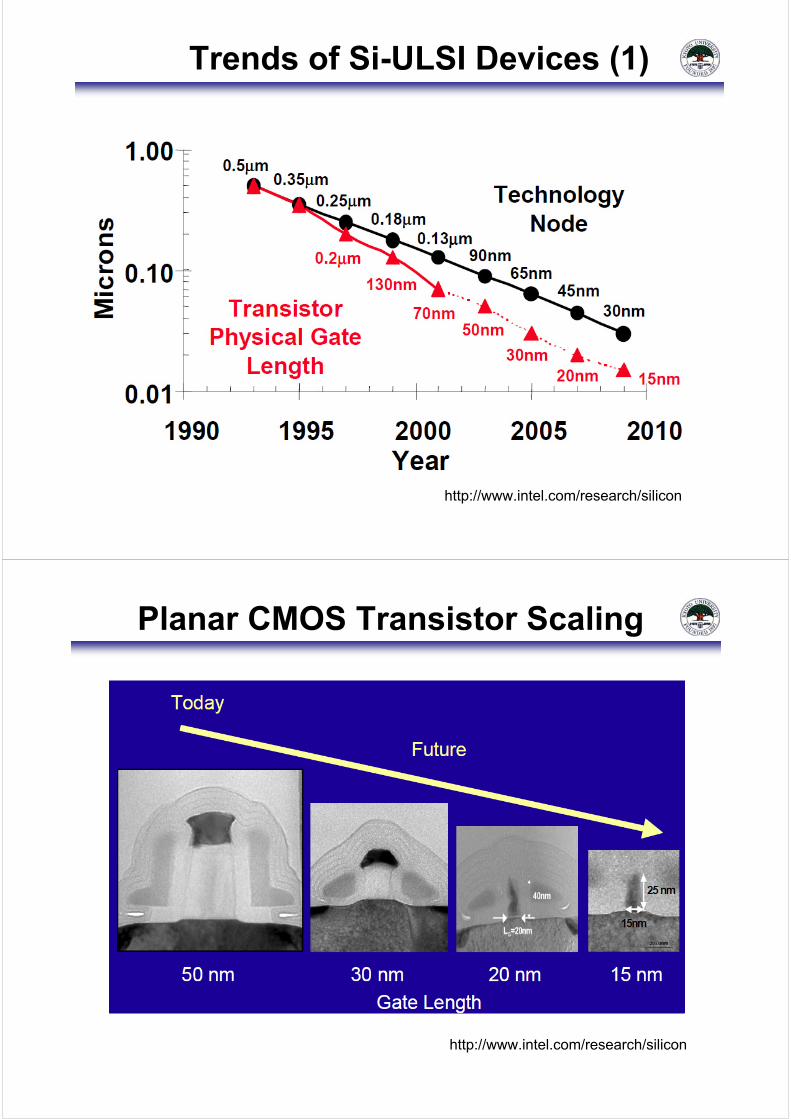
Trends of Si-ULSI Devices (1)
http://www.intel.com/research/silicon
Planar CMOS Transistor Scaling

Trends of Si-ULSI Devices (2)
MetalMetalMetalPoly-silicon
Poly-silicon
Poly-silicon
Poly-silicon
Poly-silicon
Gate electrode
High-kHigh-kHigh-kSiO2SiO2SiO2SiO2SiO2Gate dielectric
Ultra Low-k(k=1.9)
Ultra Low-k(k=2.1)
Ultra Low-k(k=2.5)
Low-k(k<2.9)
Low-k(k=2.9)
FSG(k<3.6)
FSG(k=3.6)
FSG(k=3.6)
Inter-layer dielectric
?CuCuCuCuCuAlAlInter-connect
300300300300300200/300200200Wafer size (mm)
22 nm32 nm45 nm65 nm90 nm0.13 �m0.18 �m0.25 �mProcess generation
20112009200720052003200119991997Year (1st production)
* FSG: high-density plasma fluorinated SiO2
�As integrated circuit device dimensions continue to be scaled down, increasingly strict requirementsare being imposed on plasma processing technology, including the etching and deposition of newmaterials as well as the more precise control of etching of conventional materials.�Great attention has recently been placed on integrating high and low dielectric constant (k) materials
into the fabrication of gate stacks and multi-level interconnections, respectively, for advancedsub-100 nm microelectronic devices.
High-k Gate Stack
�The technological challenge continues for growing ultra-thin SiO2 film of high quality, to maintainthe gate capacitance without increasing the leakage current and reducing the oxide reliability;however, the ultimate solution would rely on high-k materials such as HfO2 and ZrO2, and theirsilicates and aluminates. �Moreover, for gate stacks with high-k dielectrics, gate electrodes of conventional Poly-Si arerequired ultimately to be replaced by metal gates of TiN, TaN, Ru/RuO2, Pt and Ir.�Plasma processing is indispensable for the fabrication or etching of gate electrodes,and also for the removal or etching of high-k dielectric.
High-k gate stack
(from NEC)
Transistor (Gate stack)
Ultra-thin gate SiO2
(from AMAT)

Multi-level Interconnects andLow-k Inter-layer Dielectric
�Low-k inter-layer dielectrics (ILD) are required for reducing the resistance-capacitance time delay,which is getting more conspicuous as the shrinkage of the spacing between metal lines in high-density multi-level interconnections.�Plasma processing is indispensable for chemical vapor deposition (CVD) of ILD,and also for the fabrication or etching of high-aspect-ratio contact (HARC) and via holes through ILD.
(Low-k,SiOCH)
(Multi-levelinterconnects)
http://www.intel.com/research/silicon
(1) Etch anisotropy and selectivity (�)� Profile control, Critical dimension (CD) control� Selectivity over mask and underlying layers
(2) Plasma damage (�)� Charging damage� Physical damage (ion-bombardment, impurity permeation)� Radiation damage
(3) Microscopic uniformity (on a chip and cell scale) (�)� Etch rate, Profile, Selectivity, Damage, etc.� Dependence on aspect ratio (AR), feature size, and pattern density
(4) Macroscopic uniformity (on a wafer scale) (�)� Etch rate, Profile, Selectivity, Damage, etc.
(5) Etching of new materials and device structures� Low-k, High-k, Metal, Dual gate, etc.
Requirements for Plasma EtchingFor ULSI fabrication
�The ULSI devices are substantially planar (2D), usually 5-10 �m thick, owing to limitations of the traditional fabrication processes for ULSI.

In addition to (1) � (5) for ULSI,
(6) High etch rate (or Etching ofdeep structures)
(7) Etching of 3D microstructures
Requirements for Plasma EtchingFor fabrication of MEMS
�MEMS devices are manufactured using processes based on USLI fabrication technologies, and also using emerging technologies to fabricate 3D, deep (up to 1 mm) microstructures with higher throughputs and lower costs.
*MEMS: Microelectromechanical Systems
Bio-chip, �TASDNA Chip (DNA Microarrays)
SensorIR Sensor
Acceleration Sensor
Actuator
DMD (Digital MirrorDevice)
Optical Switch
RF-MEMS
Microfabrication using Etching
DRAM cell
2 mm0.2 mm
0.2 �m
Micro cantilever Micro turbine
1 �mPhotonic crystal

2. Fundamentals of PlasmaEtching Technology
� Etching Characteristics� Core Technology of Plasma Etching
Plasma reactorFeed gasProcess control
Plasma Etching Technology
� Etching Characteristics :� Etch anisotropy and selectivity� Microscopic uniformity� Plasma damage
� Plasma etching (or processing) technology consists of three coretechnologies: (1) Plasma reactor, (2) Reactive Gas, and(3) Process control.
� Plasma plays two roles in plasma processing:(1) To generate ions and reactive neutrals from feed gases through
electron impact events, which are then transported ontosubstrate surfaces.
(2) To form the sheath above substrate surfaces, which acceleratesthe ions onto substrate surfaces.

Plasma Etching
RF CoilRF PowerSource
FeedGas
DielectricPlate
Plasma
To Pump
Wafer Stage
CoolingWaterSubstrate
RF Bias
RF CoilRF PowerSource
FeedGas
DielectricPlate
Plasma
To Pump
Wafer Stage
CoolingWaterSubstrate
RF Bias
CCP* mode(100 W)
ICP Cl2 Plasma
ICP mode(300 W)
ICP (Inductively Coupled Plasma)
EtchedProfile(Poly-Si)
*CCP : Capacitively Coupled Plasma
Etch Anisotropy and Selectivity
�Anisotropy :
�CD Loss / Gain :
�Selectivity :
vertical
lateral 1ERERA ��
10 WWW ���
layerunder or mask
film
ERERS �Etching
Process
W0
W1W1
Underetch
AfterLithography
Overetch
Just Etch
After MaskRemoval
Start
MaskFilm
Substrate(Under layer)
(50% Etching)
(100% Etching)
(150% Etching)(50% Overetch)
Isotropic Anisotropic

Profile Irregularities
*The nonuniform surface coverage of neutrals results from the difference in anisotropy between incoming ions and neutral reactants.**The nonvertical ion incidence originates from the thermal motion of ions, scattering of ions through collision with neutrals in the
sheath, and deflection of ion trajectories due to charging of mask dielectrics.***The charging results from the difference in anisotropy between incoming Ions and electrons.
Microtrenching
[Ion Reflection from Feature Sidewalls][Charging of Mask Dielectrics and theConsequent Deflection of IonTrajectories]***
�Ion
(Outwardly) Tapered
[Deposition of Surface Inhibitors/Etch Products on FeatureSidewalls]
Surface Inhibitor
Etch Product
�
[Nonuniformity Surface Coverageof Neutrals in Microstructural Featurescombined with Nonvertical Ion Incidence]*
Inversely Tapered
��
Ion�Neutral Reactant
Undercut
�
Neutral Reactant
[Isotropic Etching by Neutrals]
Mask
Notching
�Ion
[Differential Charging of MicrostructuraFeatures and the Consequent Deflectionof Ion Trajectories] ***
� �� Electron��
Bowing
�Ion
[Nonvetical Incidenceof Ions]**
���
(a) (b) (c)
(d) (e) (f)
SelectivitySelectivity over underlying films is required during overetch.
MaskFilm to be etched
Just Etch
Underlying Film
Overetch
OpenField
Mask
Before Etch
Just Etch
Overetch
Before EtchFilm to be etched
Underlying Film
Mask Mask
Substrate
Selectivity overmask is requiredduring mainand overetch.

Microscopic Uniformity
(c)
(e)
(b)
(f)
(d)
[Shadowing for Incoming (Neutral) Reactants]
RIE Lag
(Neutral) Reactants
OpenField
Large aspect-ratio features etch slower than smaller ones.
OpenField
InverseRIE Lag
Surface Inhibitors
[Shadowing for Incoming Surface Inhibitors][Deposition on Bottom Surfcaes]
Large aspect-ratio features etch faster than smaller ones.
[Shadowing for Incoming (Neutral) Reactants]
RIE Lag
(Neutral) Reactants
OpenField
Large aspect-ratio features etch slower than smaller ones.[Shadowing for Incoming (Neutral) Reactants]
RIE Lag
(Neutral) Reactants
OpenField
Large aspect-ratio features etch slower than smaller ones.
OpenField
InverseRIE Lag
Surface Inhibitors
[Shadowing for Incoming Surface Inhibitors][Deposition on Bottom Surfcaes]
Large aspect-ratio features etch faster than smaller ones.
OpenField
InverseRIE Lag
Surface Inhibitors
[Shadowing for Incoming Surface Inhibitors][Deposition on Bottom Surfcaes]
Large aspect-ratio features etch faster than smaller ones.Surface Inhibitors
OpenField
[Shadowing for Incoming Surface Inhibitors][Deposition on Sidewalls]
Large aspect features etch less tapered than smaller ones.
[Transport (Redeposition) of Etch Products]
OpenField
EtchProducts
Large aspect features etch more tapered than smaller ones.
[Differential Charging of Microstructural Featuresand the Consequent Deflection of Ion Trajectories]
Notching occurs at the inner sidewall foot of theoutermost feature of a L&S structure neighboringan open area.
OpenField
Notching+
Ions+ +
OpenField
[Charging of Mask Dielectricsand the consequent Deflection of Ion Trajectories]
Large aspect features exhibit more significant trenchingthan smaller ones.
Micro-trenching
+Ions
+ +
Surface Inhibitors
OpenField
[Shadowing for Incoming Surface Inhibitors][Deposition on Sidewalls]
Large aspect features etch less tapered than smaller ones.
[Transport (Redeposition) of Etch Products]
OpenField
EtchProducts
Large aspect features etch more tapered than smaller ones.
Surface Inhibitors
OpenField
[Shadowing for Incoming Surface Inhibitors][Deposition on Sidewalls]
Large aspect features etch less tapered than smaller ones.
Surface Inhibitors
OpenField
[Shadowing for Incoming Surface Inhibitors][Deposition on Sidewalls]
Surface Inhibitors
OpenField
[Shadowing for Incoming Surface Inhibitors][Deposition on Sidewalls]
Large aspect features etch less tapered than smaller ones.
[Transport (Redeposition) of Etch Products]
OpenField
EtchProducts
Large aspect features etch more tapered than smaller ones.[Transport (Redeposition) of Etch Products]
OpenField
EtchProducts
Large aspect features etch more tapered than smaller ones.
[Differential Charging of Microstructural Featuresand the Consequent Deflection of Ion Trajectories]
Notching occurs at the inner sidewall foot of theoutermost feature of a L&S structure neighboringan open area.
OpenField
Notching+
Ions+ +
OpenField
[Charging of Mask Dielectricsand the consequent Deflection of Ion Trajectories]
Large aspect features exhibit more significant trenchingthan smaller ones.
Micro-trenching
+Ions
+ +
[Differential Charging of Microstructural Featuresand the Consequent Deflection of Ion Trajectories]
Notching occurs at the inner sidewall foot of theoutermost feature of a L&S structure neighboringan open area.
OpenField
Notching+
Ions+ +
[Differential Charging of Microstructural Featuresand the Consequent Deflection of Ion Trajectories]
Notching occurs at the inner sidewall foot of theoutermost feature of a L&S structure neighboringan open area.
OpenField
Notching+
Ions+ +
OpenField
[Charging of Mask Dielectricsand the consequent Deflection of Ion Trajectories]
Large aspect features exhibit more significant trenchingthan smaller ones.
Micro-trenching
+Ions
+ +
OpenField
[Charging of Mask Dielectricsand the consequent Deflection of Ion Trajectories]
Large aspect features exhibit more significant trenchingthan smaller ones.
Micro-trenching
+Ions
+ +
(a)
EtchRate
EtchedProfile
Plasma
photon Je Ji
electron ion
CuILD
ion
Si sub.
STISTI
gate dielectricgate electrode
PMD
ILD
ion ion
(i) Charging Damage“plasma current” : Ji , Je
(~ mA/cm2)
(ii) Physical Damageion with high energy
(Ei ~ 100 eV)
(iii) Radiation Damagehigh energy photon
(h�~ 10 eV)
(ii)(iii) (i)
Plasma
photon Je Ji
electron ion
CuILD
ion
Si sub.
STISTI
gate dielectricgate electrode
PMD
ILD
ion ion
(i) Charging Damage“plasma current” : Ji , Je
(~ mA/cm2)
(i) Charging Damage“plasma current” : Ji , Je
(~ mA/cm2)
(ii) Physical Damageion with high energy
(Ei ~ 100 eV)
(ii) Physical Damageion with high energy
(Ei ~ 100 eV)
(iii) Radiation Damagehigh energy photon
(h�~ 10 eV)
(iii) Radiation Damagehigh energy photon
(h�~ 10 eV)
(ii)(iii) (i)
Plasma Damage

Plasma Etching Reactors
5 �m 3 �m 2 �m 1.3 �m 0.8 �m 0.5 �m 0.35 �m 0.25 �m 0.18 �m 0.13 �m 90 nm 65 nm
16 K 64 K 256 K 1 M 4 M 16 M 64 M 256 M 1 G (4 G) (16G) ---
Year 1977 1980 1982 1985 1988 1991 1994 1996 1998 2001 2004 2007
6” 8” 8”/12”4” 5”WaferDiameter
Barrel type
ICP
HWP
RIE (batch type)
SWP
DCSelf-bias
�Ion-Assisted Reaction(Ion acceleration through the sheath to achievedirectional, energetic ions incident on the substrate�
�Low-Pressure, High-Density �Independent Ion Energy Control
External Magnetic Fields
Two RF/Microwave Sources: for Plasma Source and for RF Biasing
Pulse ModulationPulse BiasingFrequency ControlHigh Flow RateWall Temperature ControlWafer Temperature Control
ECR
Narrow Gap, Triode, Two-frequencyRIE(single type)
MERIE Dipole Ring Magnet
No MagneticFields
Low-Pressure, High-DensityPlasmas
ExternalMagneticFields
FeatureSize
IntegrationLevel
�Low-Pressure, High-Density �Lower Ion Energy
Feed Gas
Cooling Water GroundedElectrode(Anode)
RF Power Source
Plasma Wafer
To Pump
CoolingWater
Powered Electrode(Cathode)
Feed Gas
Cooling Water GroundedElectrode(Anode)
RF Power Source
Plasma Wafer
To Pump
CoolingWater
Powered Electrode(Cathode)
Plunger
Microwaves
Waveguide
PlasmaFeed Gas
To PumpWaferStage
Quartz Tube
Wafer
CoolingWater
Plunger
Microwaves
Waveguide
PlasmaFeed Gas
To PumpWaferStage
Quartz Tube
Wafer
CoolingWater
Cathode CouplingRIE (Reactive Ionetching)
Two-Frequency CCP
CDE (Chemical Dry Etching)
AnodeCoupling
Plasma
PoweredElectrode
GroundedElectrode
Wafer
RF Power Source(13.56 MHz)
Plasma
PoweredElectrode
GroundedElectrode
Wafer
RF Power Source(13.56 MHz)
Plasma
PoweredElectrode
Wafer
RF Power Source(40 MHz)
PoweredElectrode
RF Power Source(2 MHz)
Plasma
PoweredElectrode
Wafer
RF Power Source(40 MHz)
PoweredElectrode
RF Power Source(2 MHz)
Plasma Sources (1)
RF Power Source
Powered Electrode
Wafer
Plasma
Grounded Electrode
To Pump
Feed Gas
Powered Electrode
WaferQuartz Boat
Quartz Chamber
Etch Tunnel
RF Power Source
Powered Electrode
Wafer
Plasma
Grounded Electrode
To Pump
Feed Gas
Powered Electrode
WaferQuartz Boat
Quartz Chamber
Etch Tunnel
Barrel type(Multi Wafer Type)
CCP (Capacitively Coupled Plasma) Downstream Plasma
Low and Middle Density

RF CoilRF PowerSource
FeedGas
DielectricPlate
Plasma
To Pump
Wafer Stage
CoolingWaterSubstrate
RF BiasSource
RF CoilRF PowerSource
FeedGas
DielectricPlate
Plasma
To Pump
Wafer Stage
CoolingWaterSubstrate
RF BiasSource
Feed Gas
Cooling Water GroundedElectrode(Anode)
RF Power Source
Plasma Wafer
To Pump
CoolingWater
Powered Electrode(Cathode)
Magnetic Field Coil
Feed Gas
Cooling Water GroundedElectrode(Anode)
RF Power Source
Plasma Wafer
To Pump
CoolingWater
Powered Electrode(Cathode)
Magnetic Field Coil
RF PowerSource RF Coil
Plasma
To PumpRF Bias Source
Dielectric Wall
Substrate
CoolingWaterFeed
Gas
WaferStage
RF PowerSource RF Coil
Plasma
To PumpRF Bias Source
Dielectric Wall
Substrate
CoolingWaterFeed
Gas
WaferStage
Plasma
CoolingWater
FeedGas
To Pump Wafer Stage
RF Bias
RF PowerSource
Wafer PermanentMagnets
MagneticField Coil
Antenna
Dielectric Belljar
Plasma
CoolingWater
FeedGas
To Pump Wafer Stage
RF Bias
RF PowerSource
Wafer PermanentMagnets
MagneticField Coil
Antenna
Dielectric Belljar
MicrowavesWaveguide
DielectricWindow
FeedGas
Feed Gas
RF Bias
Wafer Stage
PlasmaWafer
CoolingWater
To Pump
ECRResonanceRegion
MagneticField Coil
MicrowavesWaveguide
DielectricWindow
FeedGas
Feed Gas
RF Bias
Wafer Stage
PlasmaWafer
CoolingWater
To Pump
ECRResonanceRegion
MagneticField Coil
Microwaves
Waveguide
Feed Gas
Grounded Plate
Wafer Stage
Cooling WaterTo Pump
RF Bias
WaferPlasma
Teflon PlateQuartz Plate
Aluminum Plate
Microwaves
Waveguide
Feed Gas
Grounded Plate
Wafer Stage
Cooling WaterTo Pump
RF Bias
WaferPlasma
Teflon PlateQuartz Plate
Aluminum Plate
ECR (Electron Cyclotron Resonance)
HWP (Helicon Wave-excited Plasma)
SWP (Surface Wave-excited Plasma)
Plasma Sources (2)MERIE (Magnetically Enhanced RIE) ICP (Inductively Coupled Plasma)
Middle and High Density
10-4 10-3 10-2 10-1 100
109
1010
1011
1012
ECP
Helicon
Gas Pressure (Torr)
Pla
sma
Den
sity
(cm
�3)
Barrel
1
RIE
MERIE
ICP
10�4 10�3 10�2 10�1 1
1012
1011
1010
109
10-4 10-3 10-2 10-1 100
109
1010
1011
1012
ECP
Helicon
Gas Pressure (Torr)
Pla
sma
Den
sity
(cm
�3)
Barrel
1
RIE
MERIE
ICP
10�4 10�3 10�2 10�1 1
1012
1011
1010
109
10-4 10-3 10-2 10-1 100
10
100
1000
1
ECR
MERIE
ICP
RIE
Barrel
��
�
��
(eV
)
Helicon
10�4 10�3 10�2 10�1 1
Gas Pressure (Torr)
Ion
Ene
rgy
(eV
)
103
102
10
10-4 10-3 10-2 10-1 100
10
100
1000
1
ECR
MERIE
ICP
RIE
Barrel
��
�
��
(eV
)
Helicon
10�4 10�3 10�2 10�1 1
Gas Pressure (Torr)
Ion
Ene
rgy
(eV
)
103
102
10
� Ion Transport through Collisionless Sheath� Low Flux of Neutral Reactants� High Flux of Ions� Low Ion Incident Energy
Plasma Properties� High Anisotropy� Little Lateral Etching� High Selectivity� Low Damage
Processing
Trends of Plasma Etching Reactors

�Halogen-containing gases are primarilyemployed for plasma etching.
�N2, O2, and CH4 gases are also employedin some cases; e.g., N2/H2 for organiclow-k films, O2/Cl2 for Ru, and CH4/H2for ITO.
�Rare gases such as He and Ar are oftenemployed as diluent gases. (Kr and Xe arealso employed in some cases.)
* Presently not used owing to toxicity problems.
*
*
Reactive Gases for Plasma Etching
From CRC Handbook of Physics and Chemistry
Bond Strengthof Diatomicmolecules
�Feed gases are preferred for etching to give reactive atoms which canbreak the bond of materials and formetch or reaction products.
+ Bond strength in eV* Bond strength in Materials
+ +
Reactive Gases for Plasma Etching(continued)

Boiling temperature of Materials (at a vapor pressure of 1 atm)
Reactive Gases for Plasma Etching
�Feed gases are preferred for etching to give reaction or etch productshaving lower boiling temperatures(or higher vapor pressures).
From CRC Handbook of Physics and Chemistry
(continued)
Process Control in Plasma Processing
Plasma Characteristics(Plasma Parameters and Structures)
Electrons: density, velocity distribution Ions and Neutrals: chemical composition,
concentration, velocity distributionPlasma Structures: plasma and surface
potentials, sheath voltage and thickness
Incident Characteristics on SubstratesIons, Neutrals, and Electrons: flux, chemical
composition, velocity distribution (Incident energy and angular distribution)
1) Gas-Phase Reactions2) Plasma-Wall Interactions
4) Plasma-Surface Interactionsin Microstructural Features
Equipment Functions (Externally Controllable Parameters)Plasma Excitation Source: frequency, power, time modulationRF Bias Source: frequency, power, time modulationFeedstock Gas: species, flow rate, pumping speed, pressure, temperatureReactor and Electrode: geometry / structure, material, temperature, external fieldsWafer / Substrate Stage: geometry / structure, material, temperature
Processing Characteristics (Etching and Deposition Characteristics)
Rate, Profile, Selectivity, Step Coverage, Electrical and Mechanical Properties, Damage, Macroscopic Uniformity, Microscopic Uniformity
Plasma Reactor
3) Plasma-Surface Interactions

3. Role of Plasma in PlasmaEtching Technology
� Gas-phase Reactions(to generate ions and neutrals)
� Ion Acceleration through the Sheath(DC self-bias voltage)
Reaction Processes in Plasma Reactor
Plasma
SheathSubstrate
Electrode (Wafer / Substrate Stage)
FeedGas To
Pump
2) Plasma-Wall InteractionsAdsorption / deposition on wallsCharge neutralization on wallsWall recombination, Wall erosion
1) Gas-Phase ReactionsElectron-impact eventsIon reactionsNeutral reactions
Ions and Neutrals Feed gas speciesProduct species
(from substrates)Impurities
(from Walls)Mask materials
3) Plasma-Surface InteractionsAdsorption, Desorption, Purely chemical reactions,Phsyical sputtering, Ion-assisted reactions,Deposition, Passivation layer formation
Transport to Substrates
�
4) Plasma-Surface Interactionsin Microstructural Features
Shadowing, Surface charging, Surface reemission/ reflection, Surface reactions
Transport to Walls
n
ChamberInner Walls(SiO2, Al2O3, etc.)
�
n
�n
w
s
PlasmaReactor
RF Source

Gas-Phase ReactionsCl/Cl2 Reaction Processes in Chlorine Plasmas
Reaction Process
Eth (eV)
Cross section (cm2)
Rate coefficienta (cm3/s)
Electron-impact reactions: Molecular ionization Dissociative ionization Ion-pair formation Dissociative attachment Dissociative excitation Atomic ionization
Electron detachment
Dissociative recombination Atomic recombination
e + Cl2 Cl2+ + e + e e + Cl2 Cl+ + Cl + e + e e + Cl2 Cl+ + Cl� + e e + Cl2 (Cl2�)* Cl� + Cl* e + Cl2 (Cl2)*
+ e Cl + Cl* + e e + Cl Cl+ + e + e e + Cl+ Cl++
+ e + e e + Cl� Cl + e + e Cl2
+ + e Cl + Cl*
Cl+ + e Cl* Cl+
+ e + e Cl* + e Cl + e Cl� Cl + e + e Cl� + e
11.48 15.48 11.87 0 3.12 13.01 23.80 3.62 0 0 �13.01 0 �3.12
�1 �2 �3 �4 �5 �6 �7 �
� � � � �
k1 k2 k3 k4 k5 k6
k7 k8=2.6�10-8 exp(�5.3/Te)
k9=9.1�10�7/Te0.6
k10=3.2�10�11/Te1/2
k11=7.1�10�7/Te9/2 cm6/s
k12=9.1�10�12/Te1/2
k13=7.1�10�7/Te9/2 cm6/s
Ion reactions: Ion-ion recombination
Charge exchange
Cl2
+ + Cl� Cl2 + Cl Cl+
+ Cl� Cl + Cl Cl+
+ Cl2 Cl + Cl2+ Cl� + Cl2 Cl + Cl� + Cl
������� ������� ������� �������
k14=5.0�10�8 k15=5.0�10�8 k16=5.4�10�10
k17=1.0�10�10
Neutral reactions: Volume recombination Wall recombination Surface reaction
Cl + Cl + M(Cl2) Cl2 + M(Cl2) Cl + Cl + wall Cl2 + wall Cl + wafer (0.25)SiCl4 + wafer
������� ������� �������
k18=2.8�10-32 cm6/s 1 =0.005 for stainless steel 2 =0.05 for silicon
a In k7-k13, the electron temperature Te is in eV. Rate coefficients k13-k17 are values at T=300 K. Coefficients 1 and 2 are reactive sticking probabilities. * Total Ionization Cross Section: Qi = �1 + �2 + �3 Total Cross section for Negative Ion Formation: Qa = �3 + �4 �1 = Qi � (�2 + �3) �3 = Qa for Ee >11.87 eV
�2 = Qi (Ee�4.0)/4 �4 = Qa for Ee <11.87 eV
or 1=0.007 *
* For anodized aluminum 1=0.1 or 0.15
Cl/Cl2 Reaction Processes in Chlorine Plasmas
Collision Cross Section Rate CoefficientElectron-Impact Reactions for Cl/Cl2
� � � �� � � � eeeeeee
eeeeee
�������
��
��
��
��
fd
vvfdvk e vv
Gas-Phase Reactions (continued)

rng
eeee
g
nkkkk
nnkknnkkkk
nknnkkkdt
d
��]Cl[]Cl[)]Cl[2]Cl[(]Cl)[]Cl[2]Cl[(
]Cl[)(])Cl[]Cl[]Cl[]Cl[(
]Cl[)2(]Cl[
171615214
13121110298
e6e542
������
������
����
�����
����
Reactants and Products0-dimensional Calculation � Cl2 Plasma �
Reactants
Plasma Diagnostics(including diagnostics of the fluxes and energiesof ions and neutrals incident on the surface).
measured
Reactants and ProductsFlux of Ions and NeutralsIncident on Substrate Surfaces
(continued)
�n � (nn/4) (8kTn /�mn)1/2
�i � 0.6ni (kTe / mi)1/2
Neutral Flux :
Ion Flux :
•The neutral-to-ion flux ratio �Cl/�i is of the order of 10at 10 mTorr, decrease wit decreasing pressure.
•The neutral-to-ion flux ratio �Cl2/�i is about one orderof magnitude higher than �Cl/�i.

Wavenumber (cm-1)
50070090011001300A
bsor
banc
e
0.000
0.004
0.008
0.012
0.016
0.020
gas phase
after Ar Plasma Treatment
during Etching
after Etching
Si-OStretch
Si-OBend
SiCl4
SiClx(x=1-3)
surface
Cl2 Plasma 0.5 mTorr
Si etching in Cl2 plasma
Plasma and Surface Diagnostics(by using FTIR absorption spectroscopy)
Reactants and Products (continued)
�Silicon tetrachloride SiCl4 was the only IR-absorbing etch product species detected in the gas phase, while unsaturated SiClx (x=1�3) as well as SiCl4 were observed on the surface.�[SiCl4] � 1�1013 cm�3 � [Cl2] in the gas phase.�A broad absorption feature due to Si�O vibrations or silicon oxides was found to occur both in the
gas phase and on the surface, where oxygen came from the dielectric windows and chamber walls.
Reaction Products (or Etch Products)
e� + SiCl4 � Cl� + SiCl3e� + SiCl4 � Cl� + SiCl2 + Cl e� + SiCl4 � Cl� + SiCl + Cl2e� + SiCl4 � Cl2
� + SiCl2e� + SiCl4 � Cl2
� + SiCl + Cl
At Ee<10 eV, k1�10�7, k2�10�7, k3�10�9, k4�10�9, and k5�10�10 cm3/s
SiCl + O2 � SiO + ClOSiCl2 + O2 � SiO + ClO + ClSiCl3 + O2 � SiO + ClO + Cl2SiCl4 + O2 � SiO + ClO + Cl2 + Cl
At T�300 K, k6�10�12, k7�10�15, k8�10�12, and k9�10�17 cm3/s
Reactants and Products (continued)
[k1][k2][k3][k4][k5]
[k6][k7][k8][k9]
Electron-Impact Reactions and Neutral reactions for Product Species
Electron-Impact Reactions
Neutral Reactions

r (cm)0 2 4 6 8 10
Neu
tral f
luxe
s (10
18 c
m��
s�� )
0.0
0.5
1.0
1.5
2.0
SiCl2SiCl4
Cl
r (cm)
r (cm)r (cm)0 2 4 6 8 10
Ion
fluxe
s (10
16 c
m�2
s�1 )
0.0
0.2
0.4
0.6
0.8
1.0
1.2
1.4
Cl2+
Cl+
Ion
Flux
(101
6cm
�2 s�1
)N
eutra
l Flu
x (1
018
cm�2
s�1
)
0.6
0.8
0.8
1.0
1.01.2
1.4
z
r0.6
0.8
0.8
1.0
1.01.2
1.4
z
r
0.20.4
0.4
0.6
0.6
0.60.8
0.8
0.8
1.0
1.0
1.0
1.2
1.2
1.2
z
r0.20.4
0.4
0.6
0.6
0.60.8
0.8
0.8
1.0
1.0
1.0
1.2
1.2
1.2
z
r
z
r
[SiCl2] (1013 cm�3)
[Cl+] (1011 cm�3)r (cm)
(a) (b)
To pump
Wafer Stage
Planar RF Coils
R=15 cm
H=9
cm
Rw=10 cm
z
r
GasInlet
Dielectric Window
RF Bias To pump
Wafer Stage
Planar RF Coils
R=15 cm
H=9
cm
Rw=10 cm
z
r
GasInlet
Dielectric Window
RF Bias
Si etching in Cl2 Plasma
Two-dimensionalFluid Simulation� Cl2 Plasma (10 mTorr) �
Reactants and Products (continued)
a) The situation is similar to Si etching in Cl2/O2 plasmas.b) Silicon oxides SiOx would also occur.c) In case of photoresist mask.
In case of hard mask (or SiO2 mask), Si and/or O would occur.
O2, OReactive species
CxHyc)SiClx, SiOxCly
b)DepositingSpecies
Surface Inhibitors
O2+, O+Cl2
+, Cl+IonCl2, ClNeutral Reactant
Mask Material
Impurity from Wallsand Windows
Reaction Product
Feed Gas
SourceRole in Surface Reactions
Reactive Speciesin Real Etching Environments
During Si etching in Cl2 plasmas a)
�In real etching environments, reactive species responsible for etching surface reactions come not only from feed gases but also reaction products, impurities from walls and/or windows, and mask materials.
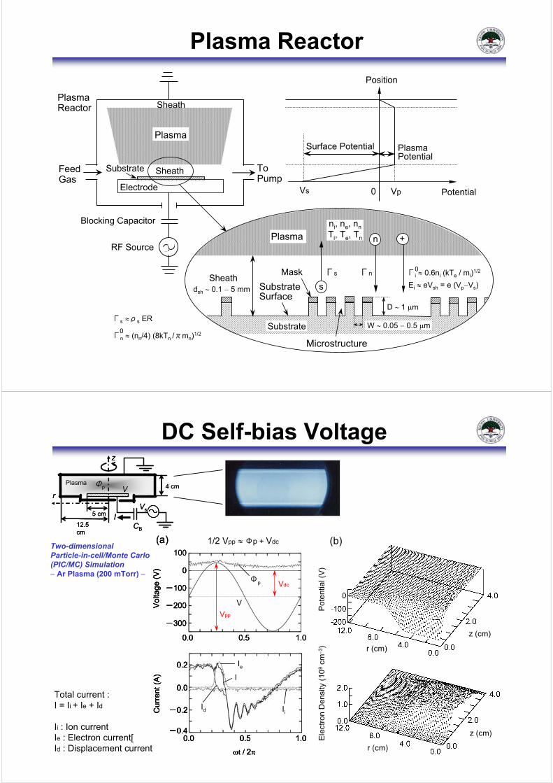
Plasma Reactor
FeedGas
0Vs Vp Potential
Position
Plasma
Sheath
Sheath
Substrate
Electrode
PlasmaReactor
PlasmaPotential
Surface Potential
ToPump
�s ��s ER
dsh � 0.1 � 5 mm
D � 1 �m
ni, ne, nn
�n
+n
W � 0.05 � 0.5 �m
s�i � 0.6ni (kTe / mi)1/2
Ei � eVsh = e (Vp�Vs)
Substrate
SubstrateSurface
Microstructure
Plasma
Sheath Mask 0
Blocking Capacitor
RF Source
�s
Ti, Te, Tn
�n � (nn/4) (8kTn /�mn)1/20
DC Self-bias Voltage
r
12.5 cm
z
4 cmPlasma �p
CB
VsI5 cm
Vr
12.5 cm
z
4 cmPlasma �p
CB
VsI5 cm
V
Total current : I = Ii + Ie + Id
Ii : Ion currentIe : Electron current[Id : Displacement current
(a)
0
Pote
ntia
l (V
)
2.012.00.0
1.0
2.0
1.0
�t / 2�
0.0 0.5�0.4
0.2
0.0
�0.2Cur
rent
(A)
Ii
I
Ie
Id
100
1.0
0
�100
�200
�300
V
0.0 0.5
Volta
ge (V
)
�p
r (cm)z (cm)
Pot
entia
l (V
)E
lect
ron
Den
sity
(109
cm�3
)
(b)
r (cm)
z (cm)
z (cm)
r (cm)
(a)
0
Pote
ntia
l (V
)
2.012.00.0
1.0
2.0
1.0
�t / 2�
0.0 0.5�0.4
0.2
0.0
�0.2Cur
rent
(A)
Ii
I
Ie
Id
1.0
�t / 2�
0.0 0.5�0.4
0.2
0.0
�0.2Cur
rent
(A)
Ii
I
Ie
Id
100
1.0
0
�100
�200
�300
V
0.0 0.5
Volta
ge (V
)
�p
0
�100
�200
�300
V
0.0 0.5
Volta
ge (V
)
�p
r (cm)z (cm)
Pot
entia
l (V
)E
lect
ron
Den
sity
(109
cm�3
)
(b)
r (cm)
z (cm)
z (cm)
r (cm)
Vdc
1/2 Vpp � �p + Vdc
Vpp
Two-dimensionalParticle-in-cell/Monte Carlo(PIC/MC) Simulation� Ar Plasma (200 mTorr) �

150 200100Energy (eV)
0.5
0.0
1.0D
istri
butio
n (a
.u.)
10 200Energy (eV)
0.5
0.0
1.0
Dis
tribu
tion
(a.u
.)
0 90Angle (deg.)
0.5
0.0
1.0
Dis
tribu
tion
(a.u
.)
30�30 60�60�9090
1.0
0Angle (deg.)
30�30 60�60�90
0.5
0.0
Dis
tribu
tion
(a.u
.) (a)
(c) (d)
(b)
Ar� e�
Ar� e�
150 200100Energy (eV)
0.5
0.0
1.0D
istri
butio
n (a
.u.)
10 200Energy (eV)
0.5
0.0
1.0
Dis
tribu
tion
(a.u
.)
0 90Angle (deg.)
0.5
0.0
1.0
Dis
tribu
tion
(a.u
.)
30�30 60�60�9090
1.0
0Angle (deg.)
30�30 60�60�90
0.5
0.0
Dis
tribu
tion
(a.u
.) (a)
(c) (d)
(b)
Ar� e�
Ar� e�
Incident Ions and ElectronsEi � �p + Vdc
Energy Distribution of Incident Ions
Cl2 Gas Pressure (Pa)
Ion Energy (eV)
Cur
rent
(re
l. un
its)
Ion Energy (eV)
Dis
tribu
tion
(a.u
.)
* Incident ion energy (or IEDF) depends on rf frequency, voltage, sheath width, ion mass, and pressure.

Incident Angle � (deg.)
-30 -20 -10 0 10 20 30
Dis
tribu
tion
G(�
)cos�
0
5
10
15
20
2050
100
500
1000
R = eVs /kTi�
Low-Pressure, High-Density Plasmas(Typically, kTi � 0.5 eV, Vsh � 50 V)
R = eVsh/kTi � 100
Incident Angle Distribution G(q) of Ion FluxesIn Collisionless Sheath
Angular Distribution of Incident Ions
Sheath
Plasma
Substrate
Maxwellian kTi
G(�)
Vsh
Ion
�
GasMolecules
� Incident angular distribution of ion fluxes (or IADF) depends on sheath voltage, sheath width, ion mass, and pressure.
4. Surface Reaction Processesin Plasma Etching(Plasma-Surface Interactions)� Surface Reactions� Transport of Ions and Neutrals
in Microstructural Features� Feature Profile Evolution� Microscopic Uniformity� Surface Charging

Etching Surface Reactions �Etching occurs through surface reactions with ions and neutrals
incident on surfaces from the plasma, where the positive ions areincident on surfaces after been accelerated through the sheath, while the neutrals are incident isotropically on surfaces.(High-energy electrons are also incident on surfaces after beingdecelerated through the sheath, playing an important role indifferential charging of feature surfaces.)
�Etching characteristics achieved depends primarily on the chemical constituent of ions and neutrals incident on surfaces, flux andenergy and angular distributions of incident ions and neutrals,and surface temperature.
�Moreover, the etching of patterned features (or the feature profile evolution during etching) are determined also by the transport of ions and neutrals in microstructural features, because the etching reactions occur in feature surfaces in microstructures
�Surface reactions responsible for etching have been investigatedby using : Beam experiments (including surface diagnostics)
Plasma experiments (including plasma and surface diagnostics,plasma simulation*) *Particle model and Fluid model
Process simulation (semi-empirical profile simulation, molecular dynamics (MD) simulation)
Study of Etching Surface Reactions
Ion Source
Gas / RadicalSource
(Ar+, Cl+, etc.)
(Cl2, XeF2, etc.)
Quartz CrystalMicrobalance / Wafer Stage
Substrate
To Pump
A+
QMS (QuadrupoleMass Spectrometer)
J.W. Coburn and H.F. Winters, J. Appl. Phys. 50, 3189 (1979).
�The etch rate is enhanced by about an order of magnitude by simultaneous exposure of ions andreactive neutrals.
Time (s)
Si e
tch
rate
(A
/min
)
XeF2 gasonly
Ar+ ion beamonly
Ar+ ion beam + XeF2 gas

Etching Mechanisms
Reaction
Desorption
Adsorption(+ mixing)
EtchingMechanism
Substrate
Purely Chemical Physical / Chemical Sputtering Ion-Assisted Inhibitor DepositionReactiveNeutral
AdsorbedNeutrals
Energetic Ion Energetic Ion (reactive) Energetic Ion
AdsorbedNeutrals
Surface Inhibitor
ReactionProduct
ReactionProduct
ReactionProductProduct
Etching Mechanism vs. Characteristics

�The etch anisotropy relies primarily on the ion-assisted reaction at the bottom of the feature andthe passivation layer formation on feature sidewalls.
�There are two mechanisms for the formation ofpassivation layers on feature surfaces:
(i) Inhibitor deposition.(ii) Inhibitor adsorption or surface oxidation.
�There are two mechanisms for ion-assisted(or ion-enhanced) reaction:
(i) Chemical sputtering (or Physically enhancedchemical sputtering), where energetic ionsenhance the step of Reaction.
(ii) Chemically enhanced physical sputtering(or Physical sputtering), where energetic ionsenhance the step of Desorption
Mechanism for Anisotropic Etching
Si Substrate
Cl+ Cl2+
Energetic Ions
Cl Cl2
��� ��� � ��� � �
ChlorosilylLayer(SiClx Layer)
Adsorption
Cl+ Cl2+
Reaction
Etch ProductsSiClx (x=1�4)
Desorption
Cl Cl2
Neutral ReactantsEnergetic Ions
���! ��� � " � "�
#� � !� � $� %&
�� � ���' �()*�+,!*
�-� ��� � �
Si
Mask
Cl Cl2
Neutral ReactantsCl+ Cl2+
Energetic Ions
SiClx
Surface InhibitorsSiClxSiOxCly
(Unreactive / Depositing Species)
(Reactive Species)O O2
Reaction Layer(SiClx Layer)
Ion-Assisted Reaction
Passivation LayerFormation
ReactionProducts Passivation Film
(SiClx, SiOx, SiOxCly Layer)
Ion-Assisted Reaction
�The etch yield depends on ion energy as Y(Ei)=A(Ei1/2�Eth1/2) at Ei< 1 keV, where A is a constant,in physical sputtering as well as ion-assisted etching reaction.�In ion-assisted etching, the etch yield depends also on neutral-to-ion flux ratio.
Ch. Steinbrucel, Appl. Phys. Lett. 55, 1960 (1989).
Neutral-to-Ion Flux Ratio (Cl / Cl+)
0 50 100 150 200
Etc
h Y
ield
(Si /
Cl+
)
0
1
2
3
4
Ei = 75 eV
Ei = 35 eV
Ei = 55 eV
measured (Chang et al.)calculated (present model)calculated (Langmuir adsorption model)
Neutral-to-Ion Flux Ratio (Cl / Cl+)
0 50 100 150 200
Etc
h Y
ield
(Si /
Cl+
)
0
1
2
3
4
Ei = 75 eV
Ei = 35 eV
Ei = 55 eV
measured (Chang et al.)calculated (present model)calculated (Langmuir adsorption model)
Etch Yield Y(Ei, � ) vs. Incident Ion Energy Ei
J.P. Chang and H.H. Sawin, J. Vac. Sci. Technol.A 15, 610 (1977).
*
*
(� = 0�)
Beam Experiments
(� = 0�)
SiAr+ + Cl2
Cl+
Ar+
F+
Ne+
0 0.5 1.0
E (keV)
ET
CH
YIE
LD
(at
oms/
ion)
3
2
1

Ion-Assisted Reaction
T. Mizutani et al., Nucl. Instrum. Methods,B7/8, 825 (1985).
�The etch yield peaks at normal incidence (� = 0�) in ion-assisted etching reaction, while it peaksat around � � 65� in physical sputtering.
Cl2+ ion beam
Ei = 1 kV
T.M. Mayer, R.A. Baker, and L.J. Whitman,J. Vac, Sci. Technol. 18, 349 (1981).
Etch Yield Y(Ei, � ) vs. Ion Incidence Angle �
(continued)
Si
Beam Experiments
Ion-Assisted Reaction (continued)
Cou
nts
(arb
. Uni
ts)
Mass Number (amu)
Ion EnergyEi = 75 eV
Ei = 250 eV
Ei = 1000 eV
SiCl4 Gas
Si+Cl+ SiCl+ SiCl2+ SiCl3+ SiCl4+
Ar+ ion beam+ Cl2 gas on Si
Beam Experiments
Ei = 500 eV
Ei = 250 eV
Ei = 100 eV
CC
MB
MBCC
S=CC+MB
SiC
lFlu
x (a
rb. u
nits
)
Time of Flight (ms)
*MB: Maxwell-Boltzmann *CC: Collision Cascade
�The amount of lower chlorinated SiClx species increases with increasing ion energy.�The velocity distribution of etch product species desorbed from surfaces changes from MB to CC,
as the ion energy is increased.
D.J. Oosatra et al., J. Apl. Phys. 63, 315 (1988)
Reaction Products

Ion-Assisted Reaction (continued)
Surface Reaction Layer (Chlorinated Surface Layer (SiClx Layer)
N. Layadi, V.M. Donnelly, and J.T.C. Lee, J. Appl. Phys. 81, 6738 (1977).
�The chlorinated surface layer consists of SiClx (x=1-3)�The thickness of SiClx layer increases with increasing ion incident energy.
Si etching in Cl2 plasmas
Surface Reaction ProcessesModel of Surface Chemistry in Real Etching Environments(Si etching in Cl2, Cl2/O2 Plasmas)
�
�� Sn0�n
So0�o
Si (s) SiClx (s)�
SiOy (s)�
Ysn�i�
Desorption
Yso�i�
Sputtering�
Coverage: �n
Oxidation
Chlorination�
Coverage: �o�
So0�oOxidation�
Cov.:1-�n-�o-�p�
SiClx (g)�
Decomposition / Reaction ���� Deposition : Redeposition :�
SiOy (g)�
Yn�i�
Dechlorination�
Si (g)�
�SiOuClv (s)
Coverage: �p
SiOuClv (g)�Yp�i�
YSi�i�
Deposition�
Sp0�p+ Sq0�q�
Sputtering�
Sputtering�
Sp0�p+ Sq0�qDeposition Deposition
Sp0�p+ Sq0�q
SiSiClx� SiOy�
Clean Surface
OxidizedSurface�
SiOuClv�Deposited Surface�
SiOuClv�Cl� O
Si Substrate
Infinitesimal Reaction Surface�
(Etching)�
�q
�p
�n 1-�n-�o-�p� �o �p�
1-�n-�o-�p�
ChlorinatedSurface�

� � � �� ��s
nn n n o p sn n i n o o n p p q q n
� � � � � �� � � � � �t
S xY Y S S S� � � � � � � � �0 0 0 01 ( )
� � � ����s
oo0 o o p so i o p p q q o
�� � � �� � � �
tS Y S S� � � � � �1 0 0
� �� ����s
pp0 p q0 q p p i p
�� � � ��
tS S Y� � � �1
� �� �ER Y Y Y� � � � � �1 1 s
i sn n so o s n o p� � � � � �
� �� �DR S S Y� � �1
0 0 pp p q q p i p� � ��
v ER DR� �
Interface Evolution Rate :
Etch and Deposition Rates :
Temporal Change of the Coverage of Infinitesimal Reaction Surfaces :
Infinitesimal Reaction Surfaces .Chlorinated SiClx Surface �nOxidized SiOy Surface �oDeposited SiOuClv Surface �pClean Si Surface /��n��o��p
Surface Coverage. 0!�n, �o, �p!1
Surface Reaction Processes(continued)
Langmuir Adsorption Kinetics Model (monolayer adsorption)
0Ion-Enhanced Etch Yield of Si : Ysn = 0.4 (Ei = 50 eV, maximum at � � 01)from a Cl+/Cl2+ ion beam study [M. Balooch et al, JVST A14, 229 (1996)].
0Total Removal Yield of Cl Adsorbed : (xYsn + Yn) = 3 (Ei = 50 eV, maximum at � � 01)determined by comparing an ion-neutral synergy model with aspect-ratio dependence data on etch rate obtained in ECR Ar/Cl2 plasmas [A.D. Bailey III et al, JVST B13, 2133 (1995)].
0Sputter Yields of Si and SiOy : Ys (�=0�) = 0.06 (maximum at � � 601)Yso (�=0�) = 0.02 (maximum at � � 601)
from Cl+/Cl2+ ion beam study [D.J. Oostra et al., Appl. Phys. Lett. 50, 1506 (1987)].[S. Tachi et al., JVST A9, 796 (1991)].
0Sputter Yield of Surface Inhibitors SiuClvOw : Yp (�=0�) = Ysn (maximum at � � 601)assumed.
0Sticking Coefficient of Neutral Reactants on Si : Sn0 = 0.55from beam study of Cl2 on Si [D.J.D.Suullivan et al., J. Phys. Chem. 97, 12051 (1993)].
* � 0.001 for Cl on Si.
0Sticking Coefficient of O on Si and SiClx : So0 = 1from beam study [J.R. Engstrom et al., Phys. Rev. B41, 1038 (1990)].
* � 0.001 for O2 on Si from beam study [J.R. Engstrom et al., Phys. Rev. B41, 1038 (1990)].
0Sticking Coefficient of Etch Products on Si, SiClx, and SiOy : Sp0 , Sq0 = 0.1 ~ 0.5 (assumed)* ! 0.002 for SiCl4 on Si from beam study [L.J. Whitman et al., Surf. Sci. 232, 297 (1990)]. * � 0.1�0.5 for SiClx+ (x=1,2; Ei =30 eV) from beam study [T. Sakai et al., 32, 3089 (1993)].* � 1 for products on themselves.
Surface Reaction ProcessesParameters for Surface Reaction Processes (Si etching in Cl2, Cl2/O2 Plasmas)
(continued)

Transport of Ions and Neutralsin microstructures
�Ions and neutrals coming from the plasma onto substrate surfaces are further transported ontosidewalls and bottom surfaces in microstractural features. Here, neutrals include reactants,etch products and by-products, surface inhibitors, and oxygen.
P
Window (�1!�!�2)
"nP
X
Y
Z
Mask
Substrate
Energetic Ions Neutral Reactants
Surface InhibitorsEtch By-Products
�i0
�d0�p
0
�n0
Ion Sheath
Bulk Plasma
Etched Surface �i (P)
�d(P)�p(P)�n(P)
# =" - �
Etch Products �qs
�1�2
#
�
�o(P)
Oxygen �o0
�q(P)
P
Window (�1!�!�2)
"nP
X
Y
Z
X
Y
Z
Mask
Substrate
Energetic Ions Neutral Reactants
Surface InhibitorsEtch By-Products
�i0
�d0�p
0
�n0
Ion Sheath
Bulk Plasma
Etched Surface �i (P)
�d(P)�p(P)�p(P)�n(P)
# =" - �
Etch Products �qs
�1�2
#
�
�o(P)�o(P)
Oxygen �o0
�q(P)
n
Neutral Shadowing
+
Ion Shadowingn
Surface Reemission of Neutrals(Knudsen Transport)
+
IonReflection
nnn n
nn
nn
Desorption of Adsorbed NeutralsDesorption of Etch Products
Charging of Feature Surfaces(Deflection of Ion Trajectories)
R
+
e
+ + +
++
+
+
- - ------
++
+++
- -------
+ + + +
(a) (b)
(c) (d)
(e) (f)
+
n
Neutral Shadowing
+
Ion Shadowingn
Surface Reemission of Neutrals(Knudsen Transport)
+
IonReflection
nnn n
nn
nn
Desorption of Adsorbed NeutralsDesorption of Etch Products
Charging of Feature Surfaces(Deflection of Ion Trajectories)
R
+
e
+ + +
++
+
+
- - ------
++
+++
- -------
+ + + +
+
e
+ + +
++
+
+
- - ------
++
+++
- -------
+ + + +
(a) (b)
(c) (d)
(e) (f)
+
Incident Angle � (deg.)
-30 -20 -10 0 10 20 30
Dis
tribu
tion
G(�
)cos�
0
5
10
15
20
2050
100
500
1000
R = eVs /kTi�
� � � � � �� �i0
i dP Gi� �� � � " ��
�
1
2 cos
� � � �� �n n0 dP � �� ( / )cos1 2
1
2 � " ��
�
� �� � � �$ %� � �� ( / ) ( ) ( ) cos cos1 2 1r Y Q Q S Q Q sn i n n nProfile P Qd� � � & &
(b) Direct incidence (Ion shadowing)
Neutral Flux Incident on Feature Surfaces :
Ion Flux Incident on Feature Surfaces :
(a) Direct incidence (Neutral shadowing)
(e) Incidence through desorptionfrom feature surfaces
(c) Incidence through surface reemission
� �� � � �$ %� �) ( ) ( ) cos cos1r Y Q Q S Q Q sn i n n n P Qd� � � & &P
Window (�1!� !�2)
"nP
X
Y
Z
Mask
Substrate
Energetic Ions Neutral Reactants
Surface InhibitorsEtch By-Products
�i0
�d0�p
0
�n0
Ion Sheath
Bulk Plasma
Etched Surface �i (P)
�d(P)�p(P)�n(P)
# =" - �
Etch Products �qs
�1�2
#
�
�o(P)
Oxygen �o0
�q(P)
P
Window (�1!� !�2)
"nP
X
Y
Z
X
Y
Z
Mask
Substrate
Energetic Ions Neutral Reactants
Surface InhibitorsEtch By-Products
�i0
�d0�p
0
�n0
Ion Sheath
Bulk Plasma
Etched Surface �i (P)
�d(P)�p(P)�p(P)�n(P)
# =" - �
Etch Products �qs
�1�2
#
�
�o(P)�o(P)
Oxygen �o0
�q(P)
Transport of Ions and Neutrals(continued)

(c) (d)
Nor
mal
ized
Flu
x �
i (P) /
�i0
0.0
0.5
1.0
1.5
Sidewall SidewallBottomTop Top
Aspect RatioD / W = 1.0
100
20
R = eVsh / kTi = 1000
0 1 2 3 4 5
Nor
mal
ized
Flu
x �
i (0)
/ �i0
0.0
0.5
1.0
1.5
1000
R = eVsh / kTi = 2050
100
(a) (b)
(a)
Surface Position
Nor
mal
ized
Flu
x �
n(P
) / �n0
0.0
0.5
1.0
1.5
With Surface Reemission
0.1
0.4
1.0
Without Reemission
(c)
Sn= 0.01
Aspect Ratio D / W0 1 2 3 4 5
Nor
mal
ized
Flu
x �
n(0)
/ �n0
0.0
0.5
1.0
1.5
Sn= 0.01
0.4
0.1
1.0Without Reemission
With Surface Reemission
(d)
Sidewall SidewallTop TopBottom
Aspect RatioD / W = 1.0
Ions
Neutrals
Ions
Neutrals
Rectangular Trench
Geometrical Shadowing�Ion shadowing�Neutral shadowing
with surface reemission
n+Ion
Neutral
Side-wall
Side-wall
Top Top
W
Bottom0
D
Geometrical Shadowingof Ions and Neutrals
Transport of Ions and Neutrals(continued)
� RIE lag occurs in (a) and (b), being suppressed in (c) with increasing oxygen flux from the plasma.� Inverse RIE lag occurs in (d) at high oxygen flux.� Sidewall tapering occurs in (b), (c), and (d) where surface inhibitors come from the plasma.
Feature Profile Evolution
X / L0.0 0.5 1.0 1.5 2.0 2.5 3.0
Y / L
-1.0
-0.5
0.0
0.5
X / L0.0 0.5 1.0 1.5 2.0 2.5 3.0
-1.0
-0.5
0.0
0.5
0.0 0.5 1.0 1.5 2.0 2.5 3.0
Y / L
-1.0
-0.5
0.0
0.5
0.0 0.5 1.0 1.5 2.0 2.5 3.0-1.0
-0.5
0.0
0.5
�n0/ �i
0 = 10, R = eVsh / kTi = 100
�p0
/ �i0
= 0.5, �o0
/ �i0
= 0.05 �p0
/ �i0
= 0.5, �o0
/ �i0
= 0.2
�p0
/ �i0
= 0, �o0
/ �i0
= 0 �p0
/ �i0
= 2.0, �o0
/ �i0
= 0
(a) (b)
(c) (d)
Si
Mask Si etching in Cl2/O2 plasmas String Model
Dep
th
Width
ER=1.0 ER=0.91
ER=0.63 ER=0.31
�Etched profiles are simulated through modeling the transport of ions andneutrals in microstructures along with surface reaction kinetics thereat.�

� RIE lag (reactive-ion-etching lag) :�Large aspect-ratio features etch slower than smaller ones.(Narrow space features etch slower than wider ones.)
Inverse RIE lag : ��Large aspect-ratio features etch faster than smaller ones.(Narrow space features etch faster than wider ones.)�The degree of inverse RIE lag increases with increasingO2 concentration in Cl2/O2 plasmas.
Microscopic Uniformity<Example 1>
Poly-Si etching in Cl2/O2 plasmas
Si etching in SF6/Ar plasmas
(continued)
�Large aspect-ratio features etch less tapered than smaller ones.(Narrow space features etch less tapered than wider ones.)
�The degree of sidewall tapering increases with increasing pressure in Cl2 plasmas.
Microscopic Uniformity
Poly-Si etchingIn Cl2 plasmas
Outwardlytaperedsidewall :
<Example 2>
(continued)

Microscopic Uniformity<Example 3> Poly-Si etching in Cl2/O2 plasmas
�Micropillar:�Miropillars often occurs
in wide space features(or small aspect-ratio features).
�Microscopic uniformity during overetch:�The thinning and breaking of thin gate oxides during overetch step
occurs preferentially in large open spaces in pure Cl2 plasmas, while in dense areas at high level O2 addition in Cl2/O2 plasmas.
(continued)
Microscopic Uniformity
W (�m)
1 10
�W
(� m
)
0.00
0.02
0.04
0.06
0.08
0.10
0.12
0.14
0.5 52
(b)25% O220%10% 0%
Poly-Si
(P
oly-
Si / S
iO2)
0
10
20
30
40
50
60
O2 / (Cl2 + O2) (%)0 10 20 30
(103 D
/min
)
0
1
2
3
4
5
6
Poly-Si / SiO2
Poly-Si
SiO2 (�2)
(a)
W (�m)
1 100.8
1.0
1.2
1.4
1.6
0.5 52
25% O2
10%
0%
0.5 5
20%
2
SiO2
(d)
W (�m)
1 100.90
0.95
1.00
1.05
1.10
1.15
1.20
25% O2
10%
0%
0.5 5
20%
2
(c)
Poly-Si
Pattern Width
Pattern WidthPattern Width
Cl2/O2 Plasma, 3 mTorrFlow rate : 60 sccmMicrowave power : 400 WRF bias power : 30 W
Nor
mal
ized
Etc
h R
ate
of P
oly-
Si
-�2
!�
34
�5
67
89:
;<
=
Etc
h R
ate
of O
pen
Spa
ce (
102
nm/m
in)
Nor
mal
ized
Etc
h R
ate
of S
iO2
Line
wid
thSh
ift �
W (�m
)Se
lect
ivity
(Po
ly-S
i/SiO
2)
W (�m)
1 10
�W
(� m
)
0.00
0.02
0.04
0.06
0.08
0.10
0.12
0.14
0.5 52
(b)25% O220%10% 0%
Poly-Si
(P
oly-
Si / S
iO2)
0
10
20
30
40
50
60
O2 / (Cl2 + O2) (%)0 10 20 30
(103 D
/min
)
0
1
2
3
4
5
6
Poly-Si / SiO2
Poly-Si
SiO2 (�2)
(a)
W (�m)
1 100.8
1.0
1.2
1.4
1.6
0.5 52
25% O2
10%
0%
0.5 5
20%
2
SiO2
(d)
W (�m)
1 100.90
0.95
1.00
1.05
1.10
1.15
1.20
25% O2
10%
0%
0.5 5
20%
2
(c)
Poly-Si
Pattern Width
Pattern WidthPattern Width
Cl2/O2 Plasma, 3 mTorrFlow rate : 60 sccmMicrowave power : 400 WRF bias power : 30 W
Nor
mal
ized
Etc
h R
ate
of P
oly-
Si
-�2
!�
34
�5
67
89:
;<
=
Etc
h R
ate
of O
pen
Spa
ce (
102
nm/m
in)
Nor
mal
ized
Etc
h R
ate
of S
iO2
Line
wid
thSh
ift �
W (�m
)Se
lect
ivity
(Po
ly-S
i/SiO
2) Linewidth Shift :�W = Wafter - Wbefore
<Example 4>
Wbefore
Poly-Si
Wbefore
Poly-Si
WafterWafter
Poly-Si etching in Cl2O2 plasmas
Etching
*Microscopic uniformity (etch rate, sidewall profile) is achieved at �10% O2 addition in Cl2/O2 plasmas.
(continued)

Passivation Layer Formation
mask
poly-Si
SiO2
mask mask
poly-Si poly-Si
vacuum vacuum
200nm500nm
Passivation layers
(a)
(b)50nm
OpenSpace
200nmspace
~11 nm
micro-trenching
Passivationlayers
~9 nm
Mask
Poly-Si
50nm
OpenSpace
200nmspace
~11 nm
micro-trenching
Passivationlayers
~9 nm
Mask
Poly-Si
mask
poly-Si
SiO2
mask mask
poly-Si poly-Si
vacuum vacuum
200nm500nm
Passivation layers
mask
poly-Si
SiO2
mask mask
poly-Si poly-Si
vacuum vacuum
200nm500nm
Passivation layers
(a)
(b)50nm
OpenSpace
200nmspace
~11 nm
micro-trenching
Passivationlayers
~9 nm
Mask
Poly-Si
50nm
OpenSpace
200nmspace
~11 nm
micro-trenching
Passivationlayers
~9 nm
Mask
Poly-Si
� XPS AnalysisK.V. Guinn, C.C. Cheng, and V.M. Donnelly,J. Vac. Sci. Technol. B13, 214 (1995).
Etched Profile and Profile Simulation �� Atomic-scale Cellular Model �
Y. Osano et al., Jpn. J. Appl. Phys. 45, 8157 (2006).
Thickness
Thic
knes
sSi etching in Cl2/O2 plasmas
�Passivation layers are formed on feature surfaces throughdeposition of surface inhibitors (primarily etch productsand by-products) and/or surface oxidation.�The thickness of passivation layers is significantly large
on feature sidewalls.
�Ion reflection on feature sidewalls is responsible for profile anomalies such as microtrenching and footing on sidewalls near the feature bottom and thereat, which are also affected by deposition of etch products and by-products and surface oxidation.
Ion Reflection
Cl+
Si
�
v0
p
L = 2.7 Å
v'
p
Vacuum Solid
rcutoff = 3.5 Å
r
Solid-vacuum interface
Cl+
Si
�
v0
p
L = 2.7 Å
v'
p
Vacuum Solid
rcutoff = 3.5 Å
r
Solid-vacuum interface
Width (nm)0.0 2.0 4.0 6.0 8.0 10.0
0.0
2.0
4.0
6.0
8.0
10.0
Si (solid)
Vacuum
Cl+ ion.(Ei = 50 eV)
incident angle�i = 751
feature sidewall
�i
xz
y
10.0
Width (nm)0.0 2.0 4.0 6.0 8.0 10.0
0.0
2.0
4.0
6.0
8.0
10.0
Si (solid)
Vacuum
Cl+ ion.(Ei = 50 eV)
incident angle�i = 751
feature sidewall
�i
xz
y
10.0
Dep
th Etched Profile Simulation � � Atomic-scale Cellular Model �Y. Osano et al., Jpn. J. Appl. Phys. 45, 8157 (2006).
Si etching in Cl2/O2 plasmas Without ion reflection on feature sidewalls
Mask
Si
SiO2
Si
Mask
Si
SiO2
Si
Mask
Si
SiO2
Si
With ion reflection on feature sidewalls
Mask
SiSiO2
Si

�Notch is a sharp undercut that occurs on feature sidewalls near the bottom of the feature. �In etching of conducting films on dielectrics (e.g., poly-Si gate etch), notching occurs during overetch
step, at the inner sidewall foot of the outermost feature of a L&S structure neighboring an open area.
�The notch is caused by the deflection of ion trajectories in microstructural features due to the localized charging of feature surfaces, which in turn originates intrinsically from the difference ofthe velocity distribution between ions and electrons incident on substrate surfaces.�Such a phenomena is known as “electron shading effect”, which causes charging damage as well as
profile anomalies.
Surface Charging
Surface ChargingProfile Simulation
�String Model�
X -axis(�m)
-0.9 -0.6 -0.3 0.0 0.3 0.6 0.9
Y -a
xis(
�m
)
3 .0
3.3
3.6
3.9
4.2
4.5
4.8
Open Area
Mask MaskPoly-Si
Dense Line-and-Space
X-axis (�m)
Y-ax
is (�
m)
X -axis(�m)
0 3e-7 6e-7
Y -a
xis(�m
)
4.5
4.6
4.7
4.8
25
8
11
14
14
X -axis(�m)0.0 0.3
Y -a
xis(�m
)
4.50
4.55
4.60
4.65
4.70
4.75
4.80
23456789
101112
131415
131415
(a)
(b)
SiO2
Doped
Pattern Area
X -axis(�m)
-0.9 -0.6 -0.3 0.0 0.3 0.6 0.9
Y -a
xis(
�m
)
3 .0
3.3
3.6
3.9
4.2
4.5
4.8
Open Area
Mask MaskPoly-Si
Dense Line-and-Space
X-axis (�m)
Y-ax
is (�
m)
X -axis(�m)
0 3e-7 6e-7
Y -a
xis(�m
)
4.5
4.6
4.7
4.8
25
8
11
14
14
X -axis(�m)0.0 0.3
Y -a
xis(�m
)
4.50
4.55
4.60
4.65
4.70
4.75
4.80
23456789
101112
131415
131415
X -axis(�m)
0 3e-7 6e-7
Y -a
xis(�m
)
4.5
4.6
4.7
4.8
25
8
11
14
14
X -axis(�m)0.0 0.3
Y -a
xis(�m
)
4.50
4.55
4.60
4.65
4.70
4.75
4.80
23456789
101112
131415
131415
(a)
(b)
SiO2
Doped
Pattern Area
Charging (1): Conductor featuresurfaces (during overetch)
(continued)
X -axis(�m )0.10 0.15 0.20 0.25 0.30 0.35
Y -a
xis(� m
)
1 .2
1.3
1.4
1.5
1.6
1.7
14
14
12
20
18
18
16
16
22
20
20
2222
22
22
X -axis(�m)-0.6 -0.4 -0.2 0.0 0.2 0.4 0.6
Y -a
xis(�m
)
0.6
0.8
1.0
1.2
1.4
1.6
Mask Mask
SiO2
X-axis (�m)
Y-ax
is (�
m)
(a)
(b)
X -axis(�m )0.10 0.15 0.20 0.25 0.30 0.35
Y -a
xis(� m
)
1 .2
1.3
1.4
1.5
1.6
1.7
14
14
12
20
18
18
16
16
22
20
20
2222
22
22
X -axis(�m)-0.6 -0.4 -0.2 0.0 0.2 0.4 0.6
Y -a
xis(�m
)
0.6
0.8
1.0
1.2
1.4
1.6
Mask Mask
SiO2
X-axis (�m)
Y-ax
is (�
m)
(a)
(b)
Charging (2): Dielectric featuresurfaces

Al etch
a) Al is etched pure-chemically in Cl2, showing no ion-assisted reaction characteristics. Thus, surface inhibitor deposition is indispensable on sidewalls to obtain anisotropic profiles of Al. Selectivity is required over photoresist mask. b) (BOCl)x is volatile.
c) Compounds of AlClx and CxHy are usually primary surface inhibitors during Al etching.
O2, OReactiveCxHy
c)AlClx, AlOxClyc)BxCly, BxOy
b)DepositingSurface Inhibitors
O2+, O+Cl2
+, Cl+, BCl+IonCl2, ClNeutral Reactant
Mask Material
Impurity from Wallsand Windows
Reaction Product
FeedGas
SourceRole in Surface Reactions
>S. Park, L.C. Rathbun, and T.N. Rhodin,J. Vac. Sci. Technol.,A 3, 791 (1985).
T. Banjo et al., Jpn. J. Appl. Phys.,36, 4824 (1997). �
Al / Ar++Cl2 Al etching in BCl3/Cl2/O2 plasmas
O2
Reactive species in Al etching with BCl3/Cl2 and BCl3/Cl2/O2 plasmas a)
SiO2 etch
a) SiO2 is etched in fluorocarbon (CF4, C4F8, etc.) plasmas with relatively high rf bias voltage; thus the etched profilesare usually anisotropic. C is indispensable in SiO2 etching through breaking strong Si�O bonds and/or oxygen removal in the form of volatile compounds such as CO. In addition, F is also indispensable for Si removal through the formation of volatile SiF4[e.g., SiO2 + 2CF + 2F � SiCl4 + 2CO].
b) Selectivity is required over Si, where fluorocarbonradicals CxFy play an important role; in some cases,H2 is added to scavenge F and thus to release orincrease surface inhibitors CxFy.
c) Surface reaction layer contains SiCxFyOz. d) Hard mask (e.g., poly-Si) is also often employed.
O2, OReactiveCxHy
d)SiFx, SiOxFyc)CxFy
b), (CFx+)DepositingSurface
Inhibitors
O2+, O+F2
+, F+, CFx+Ion
F2, FNeutral Reactant
Mask Material
Impurity from Wallsand Windows
Reaction Product
FeedGas
SourceRole in Surface Reactions
Reactive species in SiO2 etching with fluorocarbon plasmas a)
N.R. Rueger et al., J. Vac. Sci. Technol. A 15, 1881 (1997). �SiO2 etching in CHF3 plasmas

5. Current Issues of PlasmaEtching Technology� Current issues� Poly-Si gate etch� High-k gate etch
(HfO2, Dual metal gate)� Metal etch (Pt, Ru)� Deep RIE of Si
Current Issues� Etching of Conventional Materials :
� Etch anisotropy and selectivity*Profile and CD control on atomic scale*Selectivity over underlying ultra thin films*Surface roughness on atomic scale (LER+, etc.)
� Microscopic uniformity� Plasma damage
� Etching of New Materials :� Substrate : SiGe, Ge� Gate : High-k* dielectrics (HfO2, ZrO2, etc.)
/ Metal electrodes (TaN, Mo, Ru, W, etc.)� Capacitor : High-k* dielectrics (Ta2O5, BST)
/ Metal electrodes (Pt, Ir, Ru)� Inter layer dielectrics (ILD) :
Low-k dielectrics (SiOC, MSQ**, Organic)
These issues are also to be resolvedin etching of new materials
** MSQ: mechylsilsesquioxane* k: dielectric constant
+ LER: line edge roughness

(2) Selectivity�Gate Electrode (poly-Si, metal)
Mask ----- Hard mask (SiO2)Underlying Layer ------- Gate Dielectrics
�Gate Dielectric (SiO2, SiON, High-k dielectric)Mask ----- Gate Electrode ( + Mask)Underlying Layer------- Si
(4) Microscopic Uniformity� Pattern sensitivity* of feature
or profile irregularities� Pattern sensitivity of etch rate or selectivity
RIE lag, inverse RIE lag� Pattern sensitivity of damage
*feature size, aspect ratio, pattern density
(5) Macroscopic Uniformity� Wafer Uniformity
(3) Plasma Damage� Charging Damage
Gate Dielectrics (Dielectric Breakdown)Transistor (deterioration)
� Gate Dielectrics : deterioration of dielectric� Gate Dielectrics : penetrate
(1) Profile (Mainly gate electrode )� Feature. feature size?critical dimension
Minimum feature size L< 0.1 �mCD loss/gain �L< 0.01 �m (=10 nm)
� Profile irregularities. notch, microtrench, (owing to bending of ion trajectory)
*In case of hard etching materialsMore sidewall deposition � CD gain,Needs for removing of residues on sidewalls
Gate Etch
Gate Length . L< 0.1 �m, Spacing < 0.1 �mGate Electrode . Poly-Si (thickness � 300 nm)
metal (W, TiN, TaN, Pt, Ir, Ru, etc.thickness� 50�60 nm)
Gate Dielectric. SiO2, SiONHigh-k dielectric (Al2O3, HfO2, ZrO2)thickness � 1 � 2 nm
Buffer layer . Mask / Gate Electrode Gate Electrode / Gate Dielectrics
Poly-Si Gate Etch
5 s 15 s 60 s 0 s
Overetch Time
10 nm
Poly-Si
SiBrxOy
Mask
Gate Oxide
Removalof PR andBARC
SiO2(Gate Dielectric)
GateElectrode
Hard MaskBeforeEtch Poly-Si
Si
ArF Resist
BARC *HM
PRBARC
Poly-Si
Si
HM
PR
Poly-Si
Si
HM
PR
Etchingof BARC
Etchingof Mask
*BottomAnti-reflectedCoating
BARC
BARC
Poly-Si
Si
Etching of Poly-Si(Overetch)
Poly-Si
Si
HM
Poly-Si
Si
Poly-Si
Si
HM
HM
Etching of Poly-Si (Main etch)
Removalof HM
�A thin passivation layer of featuresidewalls plays a key role in achievingthe nanometer-scale control of theprofile and CD during main etch andoveretch processes.

Poly-Si Gate Etch
In the plasma etching of 10-nm-scale microstructures, the ion-enhanced etching at the bottom of the feature and the passivation layer formation on feature sidewalls are still key mechanisms to be precisely controlled.
(continued)
Main etch& Overetch:
HBr/O2 = 100/7
(b) Two-stepProcess
L0 � 70 nm L0 � 50 nm L0 � 20 nm
�L�15 nm �L�10 nm �L�13 nm
�L�3 nm �L�1 nm �L�3 nm
Si Sub.
Poly-S i
Oxide Mask
GateOxides
Main etch:HBr/O2 =100/3
Overetch:HBr/O2 =100/7
(a) One-stepProcess
High-k Gate Etch�As integrated circuit device dimensions continue to be scaled down, recent efforts have been made to replace gate silicon-oxides with silicon-oxynitridesof slightly higher dielectric constant (k), and nowadays, new high-k (>20) dielectrics or metal oxides such as Al2O3, HfO2, and ZrO2 are being developed to replace SiO2.
�In integrating these high-k dielectric materials intodevice fabrication, selective etching over theunderlying Si is required for their removalprior to forming the source and drain contacts.
�Moreover, the etching of high-k dielectrics at higheretch rates with low ion energies and/or less ionsis indispensable in mass production, for chambercleaning of the chemical vapor deposition (CVD)and atomic layer deposition (ALD) apparatusesto prepare high-k thin films.
�The etching of HfO2 films in BCl3-containing plasmaswithout rf biasing or under low ion-energy conditions,together with a wafer temperature control, would bepromising candidate for the process concerned.
High-k (~2 nm)
Si
Metal (~50 nm)
Mask
< 0.1 @m
Si
Metal
High-kMask
Si
Metal
High-kMask
Si
Metal
High-k
Metaletch
High-ketch
Maskremoval
Etching process for high-k/metal gate stacks
High-k (~2 nm)
Si
Metal (~50 nm)
Mask
< 0.1 @m
Si
Metal
High-kMask
Si
Metal
High-kMask
Si
Metal
High-k
Metaletch
High-ketch
Maskremoval
Etching process for high-k/metal gate stacks

912 *sp331 *sp360 *sp
���
ZrF4ZrCl4ZrBr4
Zr(Z=40)
970 *sp317 *sp323 *sp
HfF4HfCl4HfBr4
���
Hf(Z=72)I
�8657.65
154
� 90.2� 68.85
5.2
SiF4SiCl4SiBr4
Si(Z=14)
1276 �
255
2250 192.6 97.5
AlF3AlCl3AlBr3
Al(Z=13)
BoilingPoint (ºC)
MeltingPoint (ºC)
Halogencompound
Element
*sp: sublimation point
High-k dielectrics are generally difficult materials for etching, owing to strong metal-oxygen bonds and non-volatile etch products or halogen compounds.
Etching of High-k Materials
Physical properties of potential etch product species Bond strengths for diatomic species
8.306.735.16�
Hf-OHf-FHf-ClHf-Br
5.306.885.304.45
Al-OAl-FAl-ClAl-Br
8.036.385.11�
Zr-OZr-FZr-ClZr-Br
11.155.724.112.90
C-OC-FC-ClC-Br
8.295.734.213.813.39
Si-O Si-F Si-ClSi-BrSi-Si
8.387.855.304.11
B-OB-FB-ClB-Br
BondStrength (eV)
BondBondStrength (eV)
Bond
(from CRC Handbook of Physics and Chemistry, 1998)
�Hafnium chlorides are relatively volatile, and thus Cl is expected to be useful for removal of Hf.�Boron-oxygen bonds are relatively strong, and thus B and/or BCl species are expected to be useful
for breaking strong metal-oxygen (Hf-O) bonds.
�In BCl3/Cl2/O2 plasmas, the HfO2 etch rate was enhanced with O2 addition, being �150 nm/min at�5% O2 with a selectivity of �4 over Si and of �1.2 over SiO2. �At high O2 addition > 10%, the heavy deposition occurred to inhibit etching on all sample surfaces.
(i)
(iii)
(iv)
[Cl2]/([BCl3]+[Cl2]) (%)0 20 40 60 80 100
Etc
h R
ate
(nm
/min
)
-50
0
50
100
BCl3/Cl2 5 mTorr
HfO2
SiO2
Si
EtchDepo
[O2]/([BCl3]+[Cl2]+[O2]) (%)0 5 10 15
Etc
h R
ate
(nm
/min
)
-100
0
100
200HfO2
SiO2
Si
BCl3/Cl2/O2 5 mTorr(BCl3/Cl2 = 27.5 / 62.5)
EtchDepo
MW: 600 W (without rf biasing)
�The etching of HfO2 occurred at >20% Cl2 addition. The HfO2 etch rate was maximum at � 60% Cl2,being � 100 nm/min with a selectivity of � 10 over Si and of � 2 over SiO2.
�Note that a high etch selectivity of >50 for HfO2/Si was obtained at 40-50% Cl2 addition, with a HfO2etch rate of �50 nm/min and HfO2/SiO2 selectivity of 1.5�2, where the deposition was still dominantover the etching on Si.
HfO2 etch in BCl3
(continued)Etching of High-k

TiNWMidgap
Pt, Ir, Mo, RuP-MOSFET
TaN, TaCTi, TaN-MOSFET
Nitrides, Carbides
MetalsFET
69.1���
61.3600327180
PtF6PtF4PtCl4PtBr4
Pt(Z=78)
53���
44250763�
IrF6IrF3IrCl3IrBr3
Ir(Z=77)
229.2239.35349
95.1216265
TaF5TaCl5TaBr5
Ta(Z=73)
40�227���
25.4�86.5
> 600 *dec> 500 *dec> 400 *dec
RuO4RuO2RuF5RuF3RuCl3RuBr3
Ru(Z=44)
�136.45230
284�2539
TiF4TiCl4TiBr4
Ti(Z=22)
Boiling point (�C)
Melting point (�C)
Halogencompound
Element
*dec: decomposes
Etching of MetalsPhysical properties of potential etch product species
(from CRC Handbook of Physics and Chemistry, 1998)
Metals for high-k gate stack
NMOS PMOS
Ru
HM
TaNPolyHM
PolyTaN
�Regarding high-k/metal gate stack, one approachis to employ a single metal gate material with amidgap work function for both n- and p-MOSFETs.�However, a dual-work-function metal gate tech-nology would be preferred, because of severaldrawbacks such as high threshold voltage of thesingle metal gate material.
�Etching of Pt relies intrinsically on physical sputtering, because halogen and other compounds of Pt are not volatile; thus, the Pt sidewalls are largely tapered owing to redeposition of Pt sputtered on feature sidewalls during etching.�Etching of Ru is caused by ion-assisted reaction in O2-containing plasmas, because RuO4 is volatile
to be relatively easily desorbed from surfaces; thus, vertical sidewalls are obtained for Ru.
Metal Etch
Etched in Ar/O2 PlasmaSelectivity (Pt/SiO2) � 6
Etched in O2/Cl2 PlasmaSelectivity (Ru/SiO2) �20
A A
BC #�%+CD(E%
F%G(D%#)EH(�)C
-�2 ! IJ*K
LC#)EH(�)C
BC BC
BC BCM
NO #�%+CD(E%
NO-�2 !
NO NOM
NO NO
��$ �,
BC-�2 !
��$ �,
(continued)

Metal Etch (continued)
Dual metal gate
NMOS PMOS
Ru
HM
TaNPolyHM
PolyTaN
NMOS PMOS
Ru
HM
TaNPolyHM
PolyTaN
NMOS PMOS
Ru
HM
TaNPolyHM
PolyTaN
P-metal etch(patterning)
High-k etch(removal)
NMOS PMOS
RuPR
High-k
NMOS PMOS
RuPR
High-k
NMOS PMOS
Ru
HM
TaNPoly-SiHM
P-metal etch
N-metal/ Poly-Sideposition,HM formation
N-metal etch(patterning)
High-k/P-metaldeposition,PR formation
TaNTaN
Deep RIE* (Bosch process)Cyclic process consisting of
isotropic etching with SF6 plasmas sidewall passivation with CxFy plasmas anisotropic etching with SF6 plasmas isotropic etching with SF6 plasmasachieves an etch rate of > 10 �m/min for Si.
To fabricate 3D, deep structures with higher throughputs and lower costs
*RIE: reactive ion etching
Deep RIE� Bosch process (for MEMS) �
Movable Electrode
Beams
Fixed Electrode
P
Movable Electrode Fixed Electrode
Minimum gap: 6 �mHight: 120 �m
Minimum gap: 6 �mHight: 120 �mMovable Electrode
Beams
Fixed Electrode
P
Movable Electrode Fixed Electrode
Minimum gap: 6 �mHight: 120 �m
Minimum gap: 6 �mHight: 120 �m

Deep RIE (continued)
Mask
C4F8/Ar Plasma SF6/Ar Plasma
Ar+
SF5+
SiF4
Si substrate Si substrate Si substrate
F*
CxFy
Passivation layer formation on sidewalls (and on bottom surfaces)
Removal of passivation layerson bottom surfaces
Si etching(at bottom surfaces)
Anisotropic Etch(with low pressure,
high bias)
Isotropic Etch(with high pressure,
low bias)
SF6/Ar Plasma
Ar+
SF5+
F*
*Higher etch rates and the suppress of scallops on sidewalls are issues to be further improved.
6. Summary� Future Prospects

Nanofabrication Technology
0.1 nm(1 A)1 nm10 nm100 nm
1000 nm(1 �m)
Bottom-up approach�manipulation/rearrangement of atoms�self-assembly/re-organization of atoms
to obtain nanostructures(materials, devices, )
Top-down approach�fabrication from bulk materials
and/or thin films of the materialto obtain microstructures(devices)
A combination of top-down and bottom-up approaches will be important in nanofabrication technologies for mass production,because the bottom-up approach isnot available for mass production owing to its slow rate of fabrication.
VLSI ULSI Nanoelectronics
�Top-down approach, Bottom-up approach�
TEOSCVD
CatalystPatterning
SiO2/Si
Metal Deposition
Plasma CVD CMP
Top Metal Layer Deposition
Ti, Mo, Cr, Pt
Ni
At ~ 400 to 8001 C
J. Li, Q. Ye, A. Cassell, H. T. Ng, R. Stevens, J. Han, M. Meyyappan, Appl. Phys. Lett., 82(15), 2491 (2003).
�Bottom-up approach�
Fabrication of Nanoelectrode Arrays(CNT Nanoelectrode Array / CNT Interconnects)
The scale bars are (a) 5, (b) 3, (c) 10, (d) 2, (e) 5, (f) 10, (g) 1, (h) 0.2, and (i) 0.2 �m.

Summary
�Plasma etching is now an indispensable technology for micro- andnano-fabrication of ULSI and MEMS devices.�To meet the requirements for near-future and future devices,
the precise control of etching characteristics is further required, based on the precise control of the etching mechanisms concerned.
*Current issues / requirements for plasma etching technology have been summarized in this lecture.
�In turn, a better understanding of the physical and chemical mechanisms underlying the processing continues to be required in the gas-phase and on the surfaces,
*Ion-assisted reaction and passivation layer formation continue to be key mechanisms to be precisely controlled on surfaces.
�A combination of top-down (plasma etching) and bottom-up approaches would be important for nanofabrication technologyof <10 nm scale.
For further reading� Books *VLSI Technology, edited by S.M/ Sze (McGraw-Hill, New York, 1988).*ULSI Technology, edited by C.Y. Chang and S.M. Sze (McGraw-Hill, New York,1996).*J.D. Plummer, M.D. Deal and P.B. Griffin, Silicon VLSI Technology: Fundamentals, Practice
and Modeling (Prentice Hall, New Jersey, 2000).*K.P. Cheung, Plasma Charging Damage (Springer, Berlin, 2001).*Handbook of Advanced Plasma Processing Techniques, edited by R.J. Shul and J. Pearton(Springer, Berlin, 2000).*M.A. Lieberman and A.J. Lichtenberg, Principles of Plasma Discharges and Materials
Processing , 2nd ed. (Wiley, New York, 2005).*M. Elwenspoek and H.V. Jansen, Silicon Micromachining, (Cambridge Univ. Press, Cambridge,1998). <for MEMS>*M.J. Mandou, Fundamentals of Microfabrication: The Science of Minituarization, 2nd ed.(CRC
Press, New York, 2002). <for MMS>
� Journals :*Journal of Vacuum Science and Technology A, B (AVS/AIP)*Applied Physics Letters (AIP) *Journal of Applied Physics (AIP) *Journal of Physics D : Applied Physics (IOP) *Plasma Sources Science and Technology (IOP)*Japanese Journal of Applied Physics (JSAP)