01 hoffmann applied solar expertise
32
PROSPECTS & CHALLENGES DURING INTRODUCTION OF NEW PRODUCTS IN THE PV MARKET Winfried Hoffmann Winfried Hoffmann President EPIA bifiPV Workshop Konstanz, 23rd April 2012
-
Upload
sandia-national-laboratories-energy-climate-renewables -
Category
Presentations & Public Speaking
-
view
347 -
download
0
Transcript of 01 hoffmann applied solar expertise

PROSPECTS & CHALLENGES DURING INTRODUCTION OF NEW PRODUCTS IN THE PV MARKET
Winfried HoffmannWinfried HoffmannPresident EPIA
bifiPV Workshop
Konstanz, 23rd April 2012

Applied Solar Expertise
Dr. Winfried Hoffmann – ASEPresident EPIA
SMA Management Board Representative to the EPIA
Member of the Supervisory Board of SMA Solar Technology AG
Member of Scientific Board of FhG-ISE and Supervisory Board of ISFH and Helmholtz

Customer Needs
… and market size from a GW perspective
on-grid off-grid consumer high efficiency
Small nichemainstream Small niche
3Bruxelles, 21 March 2012. 7th EPIA Market Workshop
€/kWh €/hr light W/m² g/W
Source: Fraunhofer ISE
€/m² / aesthetics €/W flexibility W/mm²
nicheSmall niche Small niche
Berlin 120419 Thin Film

c-Si Commercial Module Efficiency
Photon 2007 Module Survey Results
19.3
16.7
15.1
13.5 13.713.3
14.2 14.4 14.4 14.414.0 13.8
13.113.7
14.3
13.312.8
12
14
16
18
20
Effi
cien
cy (%
)
Error bars show mean efficiency for all products
specialized manufacturing Standard
Cells
4Bruxelles, 21 March 2012. 7th EPIA Market Workshop
0
2
4
6
8
10
12
Sun
pow
er
San
yo
BP
LG
BC BP
Sha
rp M
ono
Sha
rp M
ulti
Kyo
cera
Sun
tech
Mon
o
Sun
tech
Mul
ti
Mot
ech
Mon
o
Mot
ech
Mul
ti
Deu
tsch
e M
ono
Deu
tsch
e M
ulti
Mits
ubsh
i
JA
Sch
ott M
ulti
Sch
ott E
FG
Effi
cien
cy (%
)
7% B
deg
rada
tion
Source: Photon International, Mar-08

Crystalline Silicon PV Module Value Chain
Poly-SiFeedstockPoly-SiFeedstock
IngotProductionIngotProduction
CellProductionCellProduction
ModuleAssemblyModuleAssembly
Distribution,Integration &Installation
Distribution,Integration &Installation
MC
Wafer orSheetProduction
Wafer orSheetProduction
5Bruxelles, 21 March 2012. 7th EPIA Market Workshop
Cz
Berlin 120419 Thin Film

New products and processes for c-Si compared to mainstream products
Mainstream „new„new
Product“ orProcess“
Poly Si
Wafer
6Bruxelles, 21 March 2012. 7th EPIA Market Workshop
Cell
Module

New products and processes for c-Si compared to mainstream products
Mainstream „new„new
Product“ orProcess“
Poly Si Gas phasedestillation &Siemens reactor
- Same -
Fluidized Bed
mg-Si (no gas phase cleaning)
Wafer
7Bruxelles, 21 March 2012. 7th EPIA Market Workshop
Cell
Module

Solar Grade
PhysicochemicalPurification Process
High-Purity Silicon For Photovoltaic Energy Conversion
8Bruxelles, 21 March 2012. 7th EPIA Market Workshop
Source: PV Silicon AG, 2006
Quarzite
CokeMG-Si
ChemicalReactionHCI
SiCl4
SiHCl3SiH2Cl2
PurificationConversion
SiHCl3
SiH4
ThermalDecompositionCVD
Mod. EG-Silicon
Grade Silicon
Berlin 120419 Thin Film
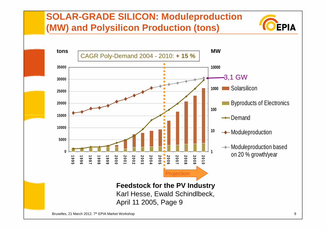
15000
20000
25000
30000
35000
100
1000
10000
Solarsilicon
Byproducts of Electronics
Demand
CAGR Poly-Demand 2004 - 2010: + 15 %
SOLAR-GRADE SILICON: Moduleproduction(MW) and Polysilicon Production (tons) AN NOT FOLLOW DEMAND – Perspectiv 2006.
tons MW
3,1 GW
9Bruxelles, 21 March 2012. 7th EPIA Market Workshop
Feedstock for the PV Industry Karl Hesse, Ewald Schindlbeck, April 11 2005, Page 9
0
5000
10000
15000
1995
1996
1997
1998
1999
2000
2001
2002
2003
2004
2005
2006
2007
2008
2009
2010
1
10
Demand
Moduleproduction
Moduleproduction based on 20 % growth/year
Projection

New products and processes for c-Si compared to mainstream products
Mainstream „new„new
Product“ orProcess“
Poly Si Gas phasedestillation &Siemens reactor
- Same -
Fluidized Bed
mg-Si (no gas phase cleaning)
Wafer mc + Cz crystal & wire saw (slurry )
Multi goes monoDiamond coated
Ribbon
10Bruxelles, 21 March 2012. 7th EPIA Market Workshop
wire saw (slurry ) Diamond coatedwire (…TFX)
Cell
Module

Wafer Production EFG Technology withRWE SCHOTT Solar (2003)
conventional Technology
solidification
melting &crystallisation
EFG Technology
Silicon ribbon pull
11Bruxelles, 21 March 2012. 7th EPIA Market Workshop 11
Wafer cuttingSi ribbonsgrowth
Laser cutting

Si ribbons (disruptive in 70ies) versus mainstream wafer cutting
� when Mobile started EFG ribbon technology, wafer cutting by ID saws used about 1 mm crystal (0.5mm kerf loss, 0.5mm waferthickness)
� with the advent of wire saws the kerf loss and the waferthickness decreased by continuous development (volume!)
12Bruxelles, 21 March 2012. 7th EPIA Market Workshop
� in addition the crystallization technology, both Cz and mc, developed further, thereby reducing the €/kg ingot significantly
� The huge expansion in poly Si production decreased the priceper kg significantly
� the small, yet existent efficiency gap (~0.5% abs) added to theend of EFG technology in 2010 (cumulative spending about 500 m€)

New products and processes for c-Si compared to mainstream products
Mainstream „new„new
Product“ orProcess“
Poly Si Gas phasedestillation &Siemens reactor
- Same -
Fluidized Bed
mg-Si (no gas phase cleaning)
Wafer mc + Cz crystal & wire saw (slurry)
Multi goes monoDiamond coated wire ribbon
13Bruxelles, 21 March 2012. 7th EPIA Market Workshop
wire saw (slurry) Diamond coated wire ribbon
Cell f-/b- screen printedcell
Selective emitterBifiMIS-IL
MWTBack cont.
Module

Main stream versus disruptive cell technology
StartStd pn
Screen printSiN passivation
Disruptive 1Bc cell(SunPower)
Disruptive 2HIT(Sanyo)
time
14Bruxelles, 21 March 2012. 7th EPIA Market Workshop
Selective emitter
New passivation, laser, …
Today cumulative experience ca 60 GW Ca 3 GWCa 2 GW

Example main stream versus disruptive
MIS-IL solar cell (ISFH/NUKEM)
� industrialization of PECVD process for SiN AR andpassivation, necessary for MIS-IL, boosted mainstream (R&R SINA)
15Bruxelles, 21 March 2012. 7th EPIA Market Workshop
� evaporation of Al was demonstrated at pilot scalebut could not be transferred to high volumeproduction (lack of equipment for cost efficientmetalization at that time … things have changed bynow!)
� … new approach with US start-up

16Bruxelles, 21 March 2012. 7th EPIA Market Workshop

High Efficiency Solar Cells
Back contact for highest current
17Bruxelles, 21 March 2012. 7th EPIA Market Workshop
n-type base

18Bruxelles, 21 March 2012. 7th EPIA Market Workshop

19Bruxelles, 21 March 2012. 7th EPIA Market Workshop

20Bruxelles, 21 March 2012. 7th EPIA Market Workshop

21Bruxelles, 21 March 2012. 7th EPIA Market Workshop

New products and processes for c-Si compared to mainstream products
Mainstream „new„new
Product“ orProcess“
Poly Si Gas phasedestillation &Siemens reactor
- Same -
Fluidized Bed
mg-Si (no gas phase cleaning)
Wafer mc + Cz crystal & wire saw (slurry)
Multi goes monoDiamond coated wire ribbon
22Bruxelles, 21 March 2012. 7th EPIA Market Workshop
wire saw (slurry) Diamond coated wire ribbon
Cell f-/b- screen printedcell
Selective emitterBifiMIS-IL
MWTBack cont.
Module Glass – EVA –backfoil & lamination
Glass – new encaps– glass (1mm)
No laminationNo encapsmaterial

From Cell to Module Production
23Bruxelles, 21 March 2012. 7th EPIA Market Workshop

New products and processes for c-Si compared to mainstream products
Mainstream „new„new
Product“ orProcess“
Poly Si Gas phasedestillation &Siemens reactor
- Same -
Fluidized Bed
mg-Si (no gas phase cleaning)
Wafer mc + Cz crystal & wire saw (slurry )
Multi goes monoDiamond coated
Ribbon
24Bruxelles, 21 March 2012. 7th EPIA Market Workshop
wire saw (slurry ) Diamond coatedwire (…TFX)
Cell f-/b- screen printedcell
Selective emitterBifiMIS-IL
MWTBack cont.
Module Glass – EVA –backfoil & lamination
Glass – new encaps– glass (1mm)
No laminationNo encapsmaterial
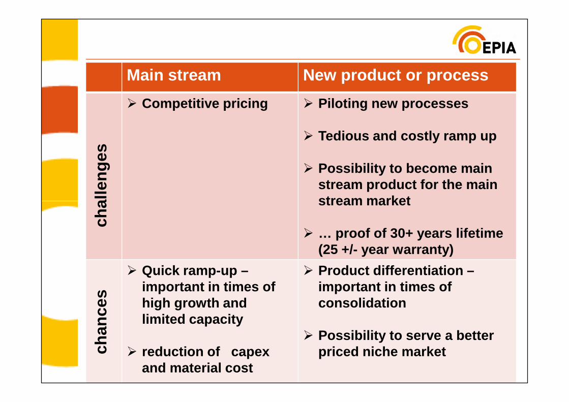
Main stream New product or process
chal
leng
es� Competitive pricing � Piloting new processes
� Tedious and costly ramp up
� Possibility to become mainstream product for the mainstream market
25Bruxelles, 21 March 2012. 7th EPIA Market Workshop
chal
leng
es
stream market
� … proof of 30+ years lifetime(25 +/- year warranty)
chan
ces
� Quick ramp-up –important in times ofhigh growth andlimited capacity
� reduction of capexand material cost
� Product differentiation –important in times ofconsolidation
� Possibility to serve a betterpriced niche market
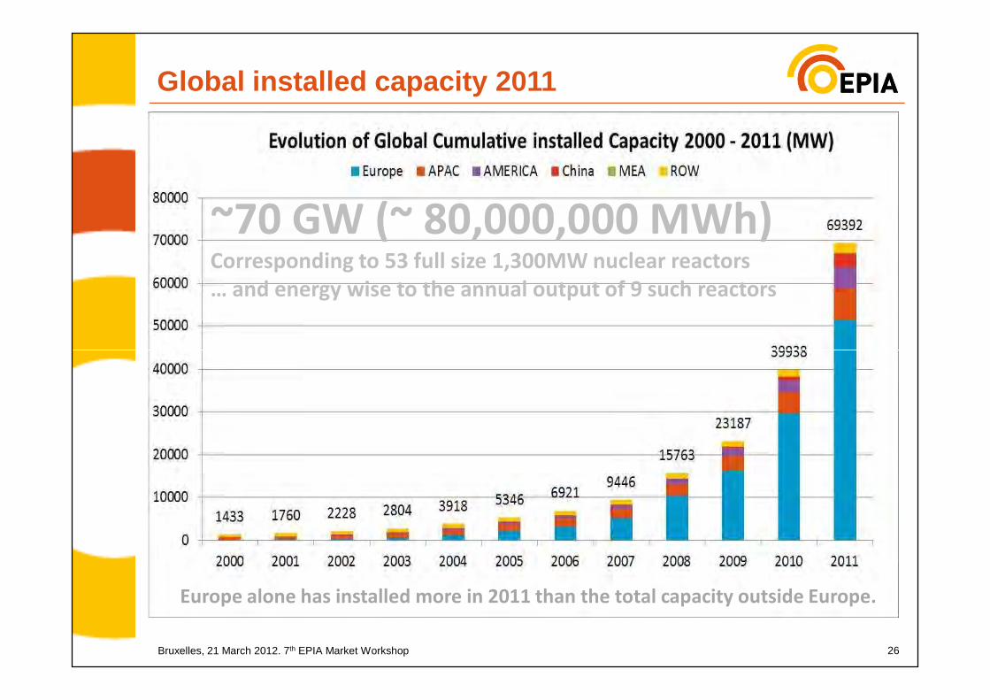
Global installed capacity 2011
~70 GW (~ 80,000,000 MWh)Corresponding to 53 full size 1,300MW nuclear reactors
… and energy wise to the annual output of 9 such reactors
26Bruxelles, 21 March 2012. 7th EPIA Market Workshop
Europe alone has installed more in 2011 than the total capacity outside Europe.
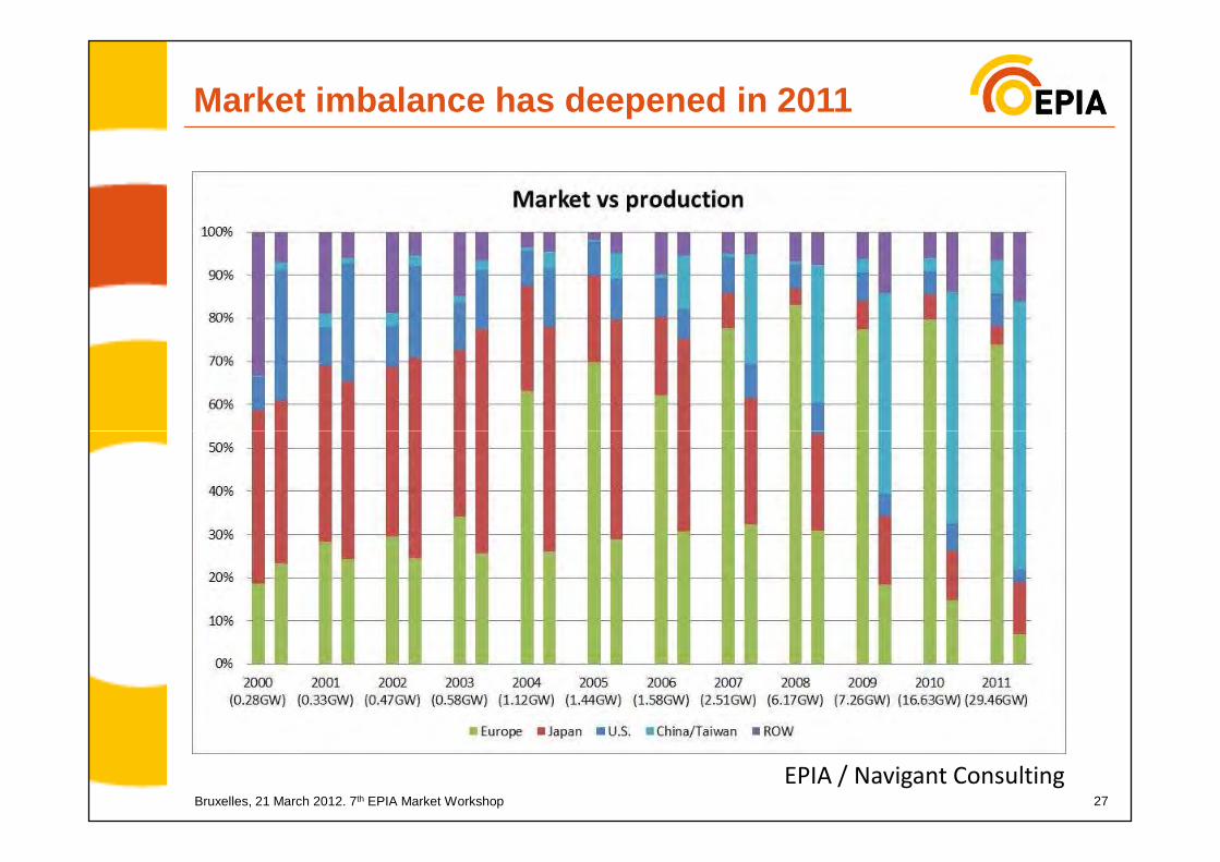
Market imbalance has deepened in 2011
27Bruxelles, 21 March 2012. 7th EPIA Market Workshop
EPIA / Navigant Consulting

1001980 2005 20081990 2000
Price Experience Curve
Photovoltaic
1. PEC for c-Si will continue
2. Reason for different PEC and PEF for Thin Film PV
28Bruxelles, 21 March 2012. 7th EPIA Market Workshop28
1
10
1,E+00 1,E+01 1,E+02 1,E+03 1,E+04 1,E+05
MW accumulated
AS
P in
$/W
PEF 20%
source: NAVIGANT
Thin Film
and PEF for Thin Film PV
3. Different growth rates forglobal PV installations asparameter
4. Different fraction of TF/c-Si as parameter

10,0
AS
P in
$/W
Case A – cSi 20%
PEC ScenarioCase A: BaselineTF share 15% constTF PEF 20%
Case B:Paradigm ShiftTF share 15% → 35%TF PEF 25%
10,0
AS
P in
$/W
Case B – cSi 20%c-Si Technology
price expectation in 2020
Photovoltaic –Future Price Development… with “healthy” module prices …
as of 2011/12
29Bruxelles, 21 March 2012. 7th EPIA Market Workshop
0,1
1,0
1,E+03 1,E+04 1,E+05 1,E+06
MW accumulated
AS
P in
$/W
Case A – TF 20%
0,1
1,0
1,E+03 1,E+04 1,E+05 1,E+06
MW accumulated
AS
P in
$/W
Case B – TF 25%
price expectation in 2020 ca. 60 – 80 $ct/W
Thin Film Technologyprice expectation in 2020
ca. 30 – 70 $ct/W

Technology Evolution
75
100
todayc-Si
TF
a-Si-pin/pin, II-VI
r/mgmc
Cz
+ (4 to 5) years *
SiIII -V
Mod
ule
pric
e (r
el. U
nits
)
r ribbon
mg metallurgicalgrade Silicon
mc multicrystalline
Cz Czochralski
30Bruxelles, 21 March 2012. 7th EPIA Market Workshop
ref: W. Hoffmann personal estimates
0 5 10 15 20 250
0 5 10 15 20 250
25
Module Efficiency [%]
a-Si/µc-Si,dye a-Si-pin
II-VI
r/mgmc
Cz+ (10 to 13) years *
50
30
Mod
ule
pric
e (r
el. U
nits
)
@ - (8 to 10) %price decrease per year
Beyond 20 years
OPV
Cz Czochralski
CPV concentrated PV
OPV organic PV
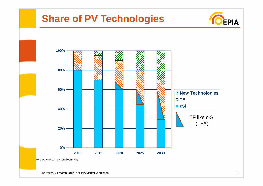
Share of PV Technologies
60%
80%
100%
New Technologies
31Bruxelles, 21 March 2012. 7th EPIA Market Workshop
0%
20%
40%
2010 2015 2020 2025 2030
New Technologies
TF
cSi
Ref: W. Hoffmann personal estimates
TF like c-Si(TFX)

www.epia.org