%0 ITbO PUTEý! TEST - Defense Technical … · HMSC-CADBIT-FR-93-2 LIST OF FIGURES Section Figure...
265
L.TR-~- 1 74 Vol if (Of two) AD-~A273 '703 CE %0 ITbO PUTEý! TEST 14ughes Missfls 3yst.wi$ Coefany ELECTE Mkia'al Dskivs, Sonny Kwar,'Tony Holzer O-I19 GM"JsAr F"~ 4cam
Transcript of %0 ITbO PUTEý! TEST - Defense Technical … · HMSC-CADBIT-FR-93-2 LIST OF FIGURES Section Figure...

L.TR-~- 1 74 Vol if (Of two)
AD-~A273 '703
CE %0 ITbO PUTEý! TEST
14ughes Missfls 3yst.wi$ Coefany ELECTE
Mkia'al Dskivs, Sonny Kwar,'Tony Holzer O-I19
GM"JsAr F"~ 4cam
t~~~~~~z4 ~~~ ~L ee.c eýt4b *V(r sratory; Puzblic Afairs ffc
PRLTR9%tlVol n Ccf toao) fla&l bemt, elw4 is 4tppwýve4 for publication.
APPROVED: £~B
?PitLceet Rgugieer
FOR THE CO!IMANDER:
ANTHONY 3. ThDUCCIA
Electromagnetica and Reliability Directorate
If tt t-d :thshndsbi iv ob e~ iI e ReaL.Mir4oi4mailng tnter adaate g a Fs~-rn~poyej býy y@&tý orjanEati~n
nc'cJ~ At~ fl~D ) riffn A~tWY 144L~ Th~zwiflasajt 1 in bmtilwr.L

REPORT DOCUMENTATION PAGE OaMB No. 0704018PWtraordi k~buiofor aim m' "d Igom gWiW otedor~f I hoU W ftva k ~dj W Ih 001 .k mchrv, bswdukVg data souces.
-1clandkz h k*owr h~.z*,2 taUbao~u re ?r da t~ d* hsr to Wu*,0w' N. aftam SarVc 04*bactr Ice klanaTT' Opeatkiorat vdReons,1215 jeftelsonOeMH MI4W. Sue 1204, j VA .=43 tWtd ID a. dMuugaweW *rdudVKw.P.wc Prj (074.0 wo, W*rn C 205021. AGENCY USE ONLY (Loav. Blani) 12 REPORT DATE a. REPORT TYPE AND DATE$ COVERED
I June 1993 IFinal - - -4. TITLE AND SUBTIITLE 5. FUNDING NUMBERSCADBIT II - C01PUTER-AIDED DESIGN FOR BUILT-IN TEST C - F306C2-90-C-0116
PE- 62702F
a AUTHOR($) PA - 0233Michael Davii, Sonny Kwan,..Tony Holzer TA- 0U
7. PERFORMING ORGMNZATION NAME(S) AND ADDRESS(ES) S. PERFORMING ORGANIZATIONHughes Missile Systems Company REPORT NUMBERP.O. Box 85357San Diego CA 92186
9. $PONSORINO/MONflORING AGENCY NAMIE(S) AND ADDRESS(ES) 10. SPONSORINGIMONITORINGRome Laboratory (ERSD) AGENCY REPORT NUMBER525 Brcoks Road flL-TR.-93-117, Vol IIGriffiss AFB NY 13441-4505 -- _______ j(of two)
11. SUPPLEMENTARY NOTES
Rome Laboratory Project Engineer: Edward L. DePalma/ERSD/(315)330-2702.
1 2a. DISTRIBUTIONAVAJLABILJTY STATEMENT It2b. DK;TRIBUT1ON CODEApproved for public release; distribution unlimited.
13. ABSTRACT (Muck,, 205Wa)The objective of CADEIT II was to develop a CAD workstation-based system with softwareto help designers incorporate Built-In Test (BIT) in their CAD-based circuit boarddesigns. The CADBIT II system consists of a Unix-based workstation, electronic CADsoftware, and the contractor-developed CADBIT 11 software module. CADBIT II benefitsprinted circuit board designers through four major functions. The. Tutorial functionincreases awareness and understanding of Built-In Test techniques. This function offerson-line access to an extensive database of information on current techniques used toimplement built-in test in digital, analog, and hybrid (mixed digital and analog) circuitboards. The Selection function helps designerý. rhoose the best technique for theirdesign. The selection log compares characterisr-;cs and attributes of each BIT techniquein the CADEIT database to information about the '-er's specific "Circuit Under Test".The CAD Insertion function helps designers imple *nt a selected BIT technique in a CADf to implement the selected BIT technique. The Evaluation function analyzes the design
impctofadding Built-In-Teat circuitry based on total board area, weight, and power11pealtes"for each BIT.
14. SUMJCT TERMS ISNUMJMER OFPACES29Computer Aided Design, Built-In-Tea-, BIT. BI29Coprtr,0~Software Design Tool, Mentor Graphics, Testability_______17. SECURITY CIASSIFICATION s.SECURITY CLAWICATION I SECURIFTY CLASSIFICATION 20L UMITATION OF ABSTRACTOFFREPORT OF 74-N PAGE OF ABSTRACTIINCIýSFE SSLST~nUN1_RVF
P'.wkxud by ANSI td Z39 '6
L.I 1

HMSC-CADBIT-FR-93-2
TABLE OF CONTENTS
Section Page
1.0 INTRODUCTION ................................................................................. 1-1
2.0 DESCRIPTION OF CADBIT fl LIBRARY CONTENT ...................... 2-12.1 LIST OF BIT TECHNIQUES ............................................... 2-12.2 ELEMENTS OF BIT LIBRARY .......................................... 2-2
3.0 BIT TECHNIQUE PACKAGES ............................................................ 3-1On-Board ROM ....................................................................................... 3-2
Microprocessor ......................................................................................... 3-17
Microdiagnostics ...................................................................................... 3-35
On-board Integration of VLSI Chip BIT (OBIVCB) ............................... 3-49
Built-in Logic Block Observer (BILBO) .................................................. 3-79
Error Detection and Correction Code (EDCC) ......................................... 3-97
Scan Design .............................................................................................. 3-115
Digital W raparound ................................................................................. 3-133
Psuedorandom Pattern Generator with Multiple Input SignatureRegister (PRPG/MISR) ............................................................................ 3-153
Comparator .............................................................................................. 3-171
Voltage Summing .................................................................................... 3-187
Redundancy .............................................................................................. 3-203
Analog Wraparound ................................................................................. 3-221
4.0 MASTER PARTS DATA ....................................................................... 4-14.1 PARTS/TECHNIQUE CROSS REFERENCE ................... 4-24.2 QUESTIONS/IECHNIQUE CROSS REFERENCE ......... 4-24.3 SUITABILITY ATTRIBUTE ............................................... 4-2
5.0 MASTER SYMBOL LIST ...................................................................... 5-1
6.0 BIT TECHNIQUE LITERATURE RESEARCH .................................. 6-1
Hii
7

HMSC-CADBIT-FR-93-2
LIST OF FIGURES
Section Figure Page
3.0
ON-BOARD ROM
I Level I Block Diagram for On-Board ROM ...................... 3-32 On-Board ROM Level II Block Diagram ............. 3-43 BIT Sequence Flow Chart for On-Board ROM ................. 3-64 On-Board ROM - Default Design ..................................... 3-115 BIT Technique Insertion Diagram for On-Board ROM ..... 3-14
MICROPROCESSOR BITI Level I Block Diagram for Microprocessor BIT ............... 3-182 Level II Block Diagram for Microprocessor BIT ............... 3-193 BIT Sequence Flow Chart for Microprocessor BIT ........... 3-224 Microprocessor BIT - Default Design ............................... 3-295 BIT Technique Insertion Diagram for
M icroprocessor BIT ........................................................... 3-32
MICRODIAGNOSTICS
1 Level I Block Diagram for Microdiagnostics ..................... 3-362 Level II Block Diagram for Microdiagnostics .................... 3-373 BIT Sequence Flow Chart for Microdiagnostics ................ 3-394 BIT Technique Insertion Diagram ..................................... 3-46
ON-BOARD INTEGRATION OF VLSI BIT CHIP (OBIVCB)
1 Level I Block Diagram for On-Board Integrationof VLSI Chip BIT ............................................................. 3-50
2 Level II Block Diagram for OBIVCB Test ProcessorN ode ................................................................................... 3-51
3 Level 11 Block Diagram for VLSI/VHSIC CUTwith BILBO ....................................................................... 3-52
4 Level II Block Diagram for VLSI/VHSIC CUTW ith Scan/Set. .................................................................... 3-53
5 BIT Sequence Flow Chart for OBIVCB ............................ 3-566 Test Processor Node Default Design for OBIVCB ........... 3-697 Scan/Set Implementation Within VLSI/VHSIC
Chip - Default Design ........................................................ 3-708 BILBO Implementation Within VLSI/VHSIC
Chip - Default Design ...................................................... 3-719 BILBO Register Detail Logic - Default Design ................ 3-7210 BIT Technique Insertion Diagram for OBIVCB ................ 3-75
iv
HMSC-CADBIT-FR-93-2
LIST OF FIGURES, Continued
Section Figure Page
BUILT-IN LOGIC BLOCK OBSERVER (BILBO)
1 Level I Block Diagram for BILBO BIT Technique ............ 3-802 Level II Block Diagram for BILBO BIT Technique .......... 3-813 BIT Sequence Flow Chart for Built-In Logic
Block Observer (BILBO) BIT Technique .......................... 3-834 BILBO - Default Design ................................................... 3-895 BILBO - Default Design ................................................... 3-906 BIT Technique Insertion Diagram - Top Level .................. 3-92
ERROR DETECTION AND CORRECTION CODE
1 Level I Block Diagram for Error Detectionand Correction Codes ......................................................... 3-98
2 Level II Block Diagram for Error Detection andCorrection Codes ................................................................ 3-99
3 BIT Sequence Flow Chart .................................................. 3-1014 EDCC - Default Design .................................................... 3-1095 BTID Block Diagram Utilizing Error Detection and
Correction Codes ................................................................ 3-112
SCAN DESIGN
1 Level I Block Diagram Scan BIT Technique ...................... 3-1162 Level II Block Diagram Scan BIT Technique .................... 3-1173 BIT Sequence Flow Chart for the Scan Design
Technique .......................................................................... 3-1194 Scan Design - Default Design ........................................... 3-1275 BIT Insertion Diagram Block Diagram Scan BIT
Technique ........................................................................... 3-130
DIGITAL WRAPAROUND
1 Level I Block Diagrmn Digital Wraparound as aBIT Technique .................................................................... 3-134
2 Level H Block Diagram Utilizing Digital Wraparound ...... 3-1353 BIT Sequence Flow Chart for Digital Wraparound ............ 3-1374 Digital Wraparound - Default Design ................................ 3-1435 Digital Wraparound BTD - Top Level ............................ 3-1466 Digital Wraparound BTID 1 - Output Buffers .................. 3-1477 Digital Wraparound BTiD 2 - Digital Gates ...................... 3-1488 Digital Wraparound BTLD 3 - Input Buffers ..................... 3-1499 Digital Wraparound BTID 4 - Pass/Fail Flip Flop ............ 3-150
V

HMSC-CADBIT-FR-93-2
LIST OF FIGURES, Continued
Section Figure Page
PSEUDORANDOM PATTERN GENERATOR WITH MULTIPLEINPUT SIGNATURE REGISTER (PRPG/MISR)
I Level I Block Diagram for PRPG/MISR ........................... 3-1542 Level II Block Diagram for PRPG/MISR BIT
Technique ........................................................................... 3-1553 BIT Sequence Flow Chart for PRPG/MISR ...................... 3-1574 PRPG/MISR - Default Design .......................................... 3-1635 BIT Technique Insertion Diagram for PRPGjMISR
BIT Technique ................................................................... 3-166
COMPARATOR1 Level I Block Diagram Utilizing Comparator as a
BIT Technique .................................................................... 3-1722 Level HI Block Diagram Utilizing Comparator as a
BIT Technique .................................................................... 3-1733 BIT Sequence Flow Chart for Utilizing Comparator
Testing Techniques for N Channels or Signals .................. 3-1754 Comparator- Default Design ............................................ 3-1815 BTID Block Diagram Utilizing Comparator
as a BIT Technique ............................................................. 3-184
VOLTAGE SUMMING
1 Level I Block Diagram for Voltage SummingTechnique .......................................................................... 3-188
2 Level II Block Diagram for Voltage SummingTechnique ........................................................................... 3-189
3 BIT Test Sequence Flow Chart for VoltageSumming BIT Technique ....................... 3-191
4 Voltage Summing- Default Design .................................. 3-1985 BIT Technique Insertion Diagram for Voltage
Summing Technique ......................................................... 3-200
REDUNDANCY1 Level I Block Diagram for Redundancy BIT
Technique ........................................................................... 3-2042 Level II Block Diagram for Redundancy BIT
Technique ........................................................................... 3-2053 BIT Sequence Flow Chart for Redundancy BIT
Technique ........................................................................... 3-2074 Redundancy - Default Design ............................................ 3-2155 BIT Technique Insertion Diagram for
Redundancy BIT Technique .............................................. 3-218
vi

HMSC-CADBIT-FR-93-2
LIST OF FIGURES, Continued
Section Figure Page
ANALOG WRAPAROUNDI Level I Block Diagram Utilizing Analog Wraparound. ...... 3-2222 Level HI Block Diagram Utilizing Analog Wraparound ..... 3-2233 BIT Sequence Flow Chart for Analog Wraparound ........... 3-2254 Analog Wraparound - Default Design ............................... 3-2315 BIT Technique Insertion Diagram for Analog
W raparound ....................................................................... 3-234
4.0
4.0 Suitability Selection M atrix ................................................ 4-3
6.0
6.0 Literature Research Results and Trends ............... 6-2
Accesiorn For
J 7
IBy**
I_ ' ,. , I
A-I/
DTIC QEIALITY -NMPECTED S
vii

H-MSC-CADBIT-FR-93-2
LIST OF TABLES
Table Page
4.0 CADB1T 11 Master Parts List (MPL) ......................................... 4-4
4.1 Component/BrT Technique Cross Reference................................. 4-5
4.2 Master Question list ........................................................... 4-6
5.0 Master Symbol List............................................................. 5-2

HMSC-CADBIT-FR-93-2
LIST OF ACRONYMS AND ABBREVIATIONS
A/D Analog-to-DigitalALS Advanced Low-Power SchottkyALU Arithmetic and Logic UnitASIC Application-Specific Integrated CihcuitBILBO Built-In Logic Block Observer
BIST Built-In Self-TestBIT Built-In TestBTID BIT Technique Insertion DiagramCAD Computer-Aided DesignCADBIT Computer-Aided Design for Built-In TestCDE Component Determination EquationCDRL Contract Data Requirements Listceil ceiling (C function to round up to nearest integer)
CLIN Contract Line Item NumberCMRR Common Mode Rejection RatioCPU Central Processing Unit
CUT Circuit Under TestD/A Digital-to-Analog
DA Differential Amplifier
DIP Dual In-line PackageECC Error Correction CodeEDC Error Detection and CorrectionEDCC Error Detection and Correction CodeEDCU Error Detection and Correction UnitEEPROM Electrically-Erasable Programmable Read-Only MemoryELIN Exhibit Line Item NumberEPROM Erasable Programmable Read-Only MemoryFF Flip-FlopFR Final Report
GMR Good Machine Responsegins gramsHMSC Hughes Missile Systems Company
IC Integrated Circuit
ix

HMSC-CADBIT-FR-93-2
LIST OF ACPONYMS AND ABBREVIATI('ONS, Continued
I/F Interface
LFSR Linear Feedback Shift Register
Lr', M Line Replaceable Module
LS Low-Power Schottky
LSI Large-Scale Integration
LSSD Level-Sensitive Scan DesignMHz Megahertz
MIL-STD Military Standard
MISR Multiple-Input Signature RegisterMSB Most Significant BitMSI Medium-Scale Integration
MUX Multiplexer
mW milliwatt
ns nanosecond
OBIVCB On-Board Integration of VLSI Chip BIT
PCB Printed Circuit Board
PISO Parallel-In, Serial-Out
PROM Programmnable Read-Only Memory
PRPG Pseudorandom Pattern Generation
RAM Random Access Memory
RF Radio Frequency
RL Rome Laboratory
RMS Root-Mean-Square
ROM Read-Only Memory
SRAM Static Random Access Memory
SSI Small-Scale Integration
S/W Software
TIM Technical Interchange Meeting
TP Test Pattern
upp units per package
URD User Requested Data
VHDL VHSIC Hardware Description Language
VHSIC Very High Speed Integrated Circuit
VLSI Very Large Scale Integration
x

HMSC-CADBIT-FR-93-2
1.0 INTRODUCTION
The Final Report was prepared as pan of contract number F30602-90-C-01 16, Computer-AidedDesign for Built-In-Test H (CADBIT 11) between Rome Laboratory (RL) and the Hughes MissileSystems Company (HMSC). This report has been prepared to satisfy the requirement for ContractLine Item Number (CLIN) 0002, Exhibit Line Item Number (ELIN) A007.
This is Volume II of the CADBIT II Final Report and contains the CADBIT II BIT LibraryPackage. This package is included to satisfy the requirements of paragraph 4.1.1 of the CADBIT IIStatement of Work (SOW). This package consists of a library of BIT techniques in a standardformat which was encoded and stored as the database of CADBIT functions.
The purpose of the CADB1T II system is to provide an automated procedure to aid the electroniccircuit designer in the selection of BIT techniques, the insertion of the associated BIT circuitry intothe Printed Circuit Boaid (PCB) design, and to provide a post design evaluation of the penaltiesincurred by the addition of BIT circuitry into the PCB functional design.
1-I
- -.
HMSC-CADBIT-FR-93-2
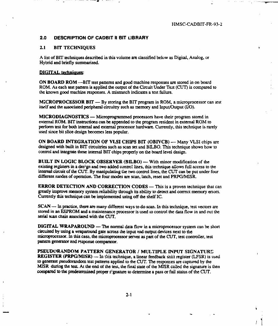
2.0 DESCRIPTION OF CADBIT II BIT LIBRARY
2.1 BIT TECHNIQUES
A list of BIT techniques described in this volume are classified below as Digital, Analog, orHybrid and briefly summarized.
DIGITAL techniques:
ON BOARD ROM -BIT test patterns and good machine responses are stored in on boardROM. As each test pattern is applied the output of the Circuit Under Teat (CUI) is compared tothe known good machine responses. A mismatch indicates a test failure.
MICROPROCESSOR BIT - By storing the BIT program in ROM, a microprocessor can testitself and the associated peripheral circuitry such as memory and Input/Output (I/O).
MICRODIAGNOSTICS - Microprogrammed processors have their program stored inexternal ROM. BIT instructions can be appended to the program resident in external ROM toperform test for both internal and external processor hardware. Currently, this technique is rarelyused since bit slice design becomes less popular.
ON BOARD INTEGRATION OF VLSI CHIPS BIT (OBIVCB) - Many VLSI chips aredesigned with built in BIT circuitries such as scan set and BILBO. This technique shows how tocontrol and integrate these internal BIT chips properly on the board level design.
BUILT IN LOGIC BLOCK OBSERVER (BILBO) - With minor modification of theexisting registers in a des;gn and two added control lines, this technique allows full access to theinternal circuit of the CUT. By manipulating the two control lines, the CUT can be put under fourdifferent modes of operation. The four modes are scan, latch, reset and PRPG/MISR.
ERROR DETECTION AND CORRECTION CODES - This is a proven technique that cangreatly improve memory system reliability through its ability to detect and correct memory errors.Currently this technique can be implemented using off the shelf IC.
SCAN - In practice, there are many different ways to do scan. In this technique, test vectors arestored in an EEPROM and a maintenance processor is used to control the data flow in and out theserial vuan chain associated with the CUT.
DIGITAL WRAPAROUND - The normal data flow in a microprocessor system can be shortcircuited by using a wraparound gate across the input nid output devices next to themicroprocessor. In this case, the microprocessor serves as part of the CUT, test controller, testpattern generator and rsponse comparator.
PSEUDORANDOM PATTERN GENERATOR / MULTIPLE INPUT SIGNATUREREGISTER (PRPG/MISR) - In this technique, a linear feedback shift register (LFSR) is usedto generate pseudorandom test patterns applied to the CUT. The responses are captured by theMISR during the test. At the end of the test, the final state of the MISR called the signature is thencompared to the predetermined proper spgnawre to determine a pass or fail status of the CUT.
2-1

HMSC-CADBIT-FR-93-2
ANALOG technimues:
COMPARATOR -- Analog test signals axe fed to the CUTY and its response is compared to awindow comparatur to determine whether the CUT is operating properly.
VOLTAGE SUMMING -- Analog signal such as dc power supply voltages can be tested inthis technique. The voltag'-s are summed using an opamp summer circuit and the output iscompared to a window comparator to determine whether the CUT is operating properly.
REDUNDANCY - The input stimulus is applied to both the CUT and the electrical equivalentof the CUT. Both output.s are fed to a diffeiential amplifie- and the difference is amnplified. Theamplified output is compared to a window comparatcr to determine pass/fail of the CUT.
HYBRID (mixed DIGITAL and ANALOGI technoques:
ANALOG WRAPAROUND -- The normal data flow in a mixed signal microprocessorsystem can be short circuited by using a wraparound analog switch across the D/A and A/Dconverters. Again, similar to the digital wraparound BIT technique, the microprocessor serves aspart of the CUT, test controller, test pattern generator and response comparator.
2.2 ELEMENTS OF BIT LIBRARY
The BIT Library contains data packltges for all of the BIT techniques available with CADB1T I.The data is used by the CADBIT H software for tutorial presentation, BIT selection, insertion andevaluation. The following is a list of the data elements with a brief description of each:
SHORT DESCRIFFION / DIAGRAMS - This is an overview and brief description of theBIT technique with high-level block diagrams. The Level I Block Diagram illustrates the basicconcept behind the BIT technique. The Level II Block diagrnm provides more functional detail andsignal flow information and shows conceptually how to implement the BIT technique and set upcorrect control signals.
FLOW CHART / DESCRIPTION - The flow chart shows the proper sequence of the BITwhen it is initiated in a typical design. It displays all the events among signal flow and componentfunction from the start of the BIT to the end of it. The description provides a step-by-step textdescription of the BIT sequence shown in the Flow Chart
ADVANTAGES - This is a list of the advantages of using the BIT technique. It describes thebenefits and design improvements in term of system reliability and testability.
DISADVANTAGES - Limitations and disadvantages of the BIT technique are explored in thissection. User can gain insight and understand the pitfalls of the technique.
2-2

HMSC-CADBIT-FR-93-2
ATTRIBUTES - There are sixteen attributes listed in this section. The first four attributes areused to determine the suitable BIT techniques in the Suitability BIT Selection Process. The area,weight, power and timing penalties are used to calculate BIT technique penalty downstream. Theother attributes are general information related to the BIT technique.
ConcurrencyTechnologyCUT Microprocessor Required?CUT Internal Design Required?Area PenaltyWeight PenaltyPower PenaltyTiming PenaltyReliability ImpactConceptual ComplexityHardware / Software / FirmwareDesign CostMemory RequirementsBIT Circuitry Self-TestableStand-alone (Self-Contained) BIT?Notes
DEFAULT DESIGN -- The Default Design includes a complete schematic built using MentorGraphics Version 8 software, and a text desciption of the design.
BIT TECHNIQUE INSERTION DIAGRAM (BTID) - The BTID is a tool to assist usersduring the insertion process. It assists users in inserting BIT components and connecting theminto the iunctional design. The diagram is supplemented with connection instructions to guideusers in connecting BIT components to the target design. New users of CADBIT II will find thisassistance valuable.
VARIABLE DEFINITIONS - CADBIT II needs this information about the Circuit UnderTest so that it can generate the BIT Technique Penalty Report. The User Requested Data windowis a list of questions merged from the Master Question List required by all the suitable BITs.
COMPONENT DETERMINATION EQUATIONS (CDE) - Equations to calculate thenumber of units (as represented by individual CAD symbols) and component parts (physicalpackages) required to implement the BIT technique using the Default Design. A single 'and' gatewould be an example of a unit. The Unit Determination Equations allow the correct number ofcomponent symbols to be. popped up in Design Architect during BIT insertion. Based on howmany units of a device type are needed and how many units in a package, the ComponentDetermination Equation calculates the number of packages required. A quad '2-input and' gate54ALS08 has four anits in it. The CDE provides the correct number of packages for area, powerand weight calculations during BIT penalty ranking process.
PENALTY EQUATIONS - Penalties for board area, weight, typical power, test time, andthroughput delay are defined. Test time is the amount of time required to perform the BIT.Throughput delay is tie induced timing delay for signal flow caused by the additional BITcircuitry.
2-3

HMSC-CADBrI'-FR-93-2
3.0 BIT TECHNIQUE DATA PACKAGES
This section contains data packages for the following BIT techniques, in the order shown below.
On.board ROMMicroprocessorMicrodiagnosticsOn-board Integration of VLSI Chip BrT (OBIVCB)Built-in Logic Block Observer (BILBO)Error Detection and Correction Ctde (EDCC)Scan DesignDigital WraparoundPseudorandom Pattern Generator with Multiple Input Signature Register (PRPG/MISR)ComparatorVoltage SummingRedundancyAnalog Wraparound
3-1

HMSC,.CADBIT-FR-93-2
ON-BOARD ROM
BIT TECHNIQUE DATA PACKAGE
CATEGORY: SHORT DESCRIPTION / DIAGRAMS
On-Board Read Only Memory (ROM) Self-Test is a nonconcunient Built-Tn-Test (BIT) techniqueimplemented in hardware and firmware. The technique consists of applying test patterns that arestored in an on-board ROM to a Circuit Under Test (CUT), and then comparing the CUTrsresponse to what is expected, resulting in a go - no/go output signal. Each test pattern can beindividually and selpctively determined, thereby maximizing the percentage of fault coverage whileminimizing the number of test patterns.
Figures 1 and 2 provide Level I and II Block Diagrams for this BIT technique.
3-2 On-Board ROM
- H

HMSC-CADB IT-FR-93-2
0
e..
3 C- 0
930
3-3 O-Boad R0

HMSC-CAE)BIT-.FR-93-2
C"j
cm,
0
ccI
3-4 On-Board ROM

HMSC-CADBIT-FR-93-2
BIT TECHNIQUE: ON-BOARD ROM
CATEGORY: FLOW CHART / DESCRIPTION
See Figure 3 for On-Board ROM Flow Chart.
1. A negative pulse 'Test Initiate" signal is input to test control logic to begin test. The testbegins as follows:
"* "BIT Mode" signal from control logic to multiplexer is activated
"* Normal inputs/outputs to/from CUT multiplexed out
"* Test Patterns (TP) from TP ROM input to CUT enabled
"* ADl resetable logic of CUT reset
"• Counters are preset
"• Pass/Fail Flip-Flop (FF) reset to Pass
"• Ensure CUT stable at falling edge of test clock. The test clock, while in BIT mode,increments the control logic counters which address the TP & GMR (Good MachineResponse) ROMs simultaneously.
2. The TP ripples through the CUT.
3. After enough delay for a test pattern to establish a response at the CUTs output and becompared with the corresponding GMR, the inverted TEST CLOCK clocks the Pass/FailFlip Flop to latch in the result.
4. A good machine at this time will have the GMR pattern identically compare with the CUToutputs. If not, the Pass/Fail FF will be set to "Fail" and will remain "Fail" until BIT is re-initiated.
5. If the address to the ROMs is the last address, then "End Of Test" control logic signal goeshigh, causing the BIT mode FF to reset and the system is out of BIT mode. The Pass/FailFF will remain set to "Pass" if during the test it was never set to "Fail".
6. If not the last ROM address, increment the counter, apply the next TP and go to step 4. If atthe last TP address, the RCO signal is triggered from most significant counter to end the test.
3-5 On-Board ROM

HMSC-CADB IT- FR-93 -2
BIT INITIATE!
INITIALIZE CUT, RESETPASS / FAIL PP TO PASS
PRE.-SET COUNTER
EAPPLY TP & GMRRO
ADDRESSES
TP RIPPLE THRU CUT JDELAY AND CLOCK
PASS/FAIL PP
NO274_844_51FigureSS 3AI BIFeuneFoFhatfrO-or O
3-6 ~On-or FAI M

HMSC-CADBIT-FR-93-2
BIT TECHNIQUE: ON-BOARD ROM
CATEGORY: ADVANTAGES
1. An understanding of the CUT can lead to a substantial percentage of fault detected with afew, predetermined test patterns.
2. A CUT with much sequential logic requires specific "Pairs" of test patterns applied insequence. Although this presents a problem with random test pattern application, storing thetest patterns in ROM so that they indeed do occur in pairs is done without difficulty with theOn-Board ROM method. Also, specific GMRs (Good Machine Responses) can be generatedby CAD circuit simulation with relative ease.
3. On-Board ROM Test Generation becomes competitive when compared to random patterngeneration as the number of CUT inputs become large and/or number of patterns requiredbecomes small. This is best understood by considering that the total number of binarypatterns possible for a CUT with n inputs is 2n. If n=16; 2n = 65,536. If n=20;2n=1,048,576. If n=24; 2n=16,777,216. Consider a 24-input CUT that can be adequatelytested with 2,000 deterministic patterns (excluding all zero pattern). To be absolutely sure ofproviding all 2,000 test patterns one must cycle through 16,777,215 (2n -1) possible testpatterns when using random pattern generator.
4. The control logic for the On-Board ROM technique is simple when compared to the randompattern generation test method which requires loading seed patterns and special testsequencing.
CATEGORY: DISADVANTAGES
1. With the growing complexity of electronic circuitry being implemented on Line ReplaceableModules (LRM) of today, it is becoming more and more difficult for a test engineer tounderstand what he is testing, especially when under pressure to establish the test planquickly. Without a true understanding of what is to be tested, it is nearly impossible todetermine the test patterns that are necessary to completely and efficiently test the CUT.
2. When the number of test patterns required to obtain adequate fault coverage is large and/orthe number of CUT inputs is small or can be partitioned into a few small number of inputgroups, then the real estate required for the On-Board ROM method becomes excessive whencompared to the random pattern generation method.
3. Circuit design changes often require reprogramming the ROMs.
4. If the number of bus lines required to address the ROMs are excessive and/or the distancebetween the TP ROMs and the control logic, or between the GMR ROMs and the controllogic is substantial, then Printed Circuit Board (PCB) real estate consumed is excessive andcostly.
5. Memory allocated to either store test patterns or GMRs can never serve both test and functionpurposes as can shift registers used in Built in Logic Block Observers (BILBO), forexample.
6. CUT and BIT logic throughput delays constrain maximum clock rate during test.
3-7 On-Board ROM

HMSC-CADBIT-FR-93-2
BIT TECHNIQUE: ON-BOARD ROM
CATEGORY: ATTRIBUTES
I. CONCURRENCY
- Nonconcurrent
2. TECHNOLOGY
* Digital
3. CUT MICROPROCESSOR REQUIRED?
* No
4. CUT INTERNAL DESIGN REQUIRED ?
- No
5. AREA PENALTY
* Increases with CUT complexity
6. WEIGHT PENALTY
* Increases with CUT complexity
7. POWER PENALTY
• Increases with CUT complexity. To minimize power penalty, use ROMs that have powerdown mode.
8. TIMING PENALTY
"* Test Time = Number of Test Patterns divided by TP application rate.
"• Throughput Delay Additional delay of MUX
3-8 On-Board ROM

HMSC-CADBIT-FR-93-2
BIT TECHNIQUE: ON-BOARD ROM
CATEGORY: ATTRIBUTES, Contd
9. RELIABILITY IMPACT
Proportional -to Area Penalty if similar technology is used for Built-In-Test Equipment(BITE) as for CUT.
- May have to distinguish BITE failures that only effect BITE vs BITE failures that effectCUT.
* Computer-Aided Design (CAD) System may have software package for reliabilitycalculation.
10. CONCEPTUAL COMPLEXITY
- Straightforward
11. HARDWARE/SOFTWARE/FIRMWARE
& Test Patterns are stored as Firmware in ROM
12. DESIGN COST
"* Use standard estimating procedure based on number of chips.
• Engineering time to create Test Patterns
"• Debug time to verify proper operation.
13. MEMORY REQUIREMENTS
* Proportional to number of test patterns and type of ROM chip.
14. BIT CIRCUITRY SELF-TESTABLE ?
0 Can do checksum on ROMs with added hardware.
15. STAND-ALONE (SELF-CONTAINED) BIT?.
* Yes
16. NOTES
* None
3-9 On-Board ROM

"HMSC-CADBIT-FR-93-2
BIT TECHNIQUE: ON-BOARD ROM
CATEGORY: DEFAULT DESIGN
This section describes the sequence of events for the ONBOARD ROM BIT technique default
design. Refer to Figure 4 for the Default Design schematic.
1. At the beginning of the test, the TEST_INITIATE signal goes low and triggers the following:
a. At the falling edge of the TESTINiTIATE signal, U2A test control flip-flop outputshigh to enable TEST_CLOCK signal to activate counters.
b. While the TEST_INITIATE signal holds low, the next rising edge of theTEST CLOCK signal loads in the preset value (beginning address) for thesynchronous 4-bit binary counters U4, U5, U6, and U7.
c. Disables normal inputs of CUT. Configures U9 and U 10 MUX to select inputs fromTest Pattern ROM to CUT.
d. Disables U13A and U13B octal buffers and places the outputs of the CUT into highimpedance.
e. Resets all resemble logics in the CLUT.
f. Presets the Pass/Fail flip-flop U2B to PASS (use _Q output).
2. After the TEST_INiTIATE signal goes back to high, the TEST_CLOCK signal startsincrementing counters U4, U5, U6, and U7. While the counters are driven directly byTESTCLOCK signal, the result of the comparison of Good Machine Response and testresponse is captured at the falling edge of the TEST_CLOCK signal to ensure enough delaytime for the test pattern to ripple through the CUT before it reaches the 8-bit identitycomparator.
3. At the end of the test, U7/RCO outputs a high and triggers the following:
a. Clears U2A test control flip-flop and disconnects the TESTCLOCK signal tocounters.
b. Enables normal inputs of CUT. Configures U9 and U10 MUX to select inputs fromnormal inputs to CUT.
c. Enables UI3A and U13B octal buffers for normal CUT outputs.
d. Any failure occuring during the test is captured by the Pass/Fail flip-flop U2B.
4. The circuit resumes normal operation and it will go into test mode when theTEST_INITIATE signal goes low again.
3-10 On-Board ROM
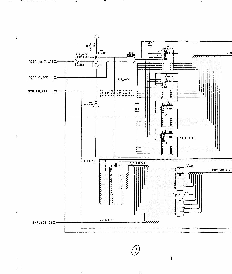
U434AL S 1S I1
VIA -CLI34A-'54 V3ALOAD NCO
*% CLI
TEST CLOCK T C> C 4ASII
I~~ ANT G
C CC
0 4

ILMSC-CADBIT-FR-93-2
NOTE, All ectocatcm, I s 45Vmed.e throslbI K poll-vp
AtI 15t01
27256 122
-As
At 5
Is I14 0444LS I3
54A*Sl
CP
'I
'S2541. S52 I7
PCP?PS
PS : 1--L- P SS FPtL~2 54L14 12
owl 4I T-TN-EPT
16 C UIT A,
AS V3YPTAMUX7:O A457
TpTRNREP(V130
jI:PU CUT 7 0
Figurt 4 On-Board ROM - Default Design
3-11/12On-Board ROM

HMSC-CADBIT-FR-93-2
BIT TECHNIQUE: ON-BOARD ROM
CATEGORY: BIT TECHNIQUE INSERTION DIAGRAM
Figure 5 shows the BIT Technique Insertion Diagram for this BIT technique.
BIT ELEMENT I
Connect the MUX output to the CUT inputs.
BIT ELEMENT 2
Connect normal LRM (Line Replaceable Module) inputs and the TP (Test Pattern) Romoutputs to the MUX inputs.
BIT ELEMENT 3
Connect the CUT outputs to the BUFFER inputs
BIT ELEMENT 4
Connect the CUT outputs to the COMPARATOR inputs.
BIT ELEMENT 5
Connect the GMR (Good Machine Response) ROM outputs to the COMPARATOR inputs.
BIT ELEMENT 6
Connect the COMPARATOR outputs to the PASS/FALL FLIP FLOP.
BIT ELEMENT 7
1. Connect the counter outputs to the address lines of the TP & GMR ROMs.
2. Tie counters preset inputs to load the beginning address of BIT routine.
3. Connect TEST INITIATE to BIT mode FLIP FLOP and PASS/FAIL FLIP FLOP.
4. Use TEST CLOCK to clock counters and invert the TEST CLOCK to clock PASS/FAIL FF.The falling edge of the TEST CLOCK signal triggers the PASS/FAIL FiV after the totalsettling time of the circuiL
5. Set up RCO signal from most significant counter to indicate END OF BIT, disable BITcircuitry and return CUT to normal operational mode.
3-13 On-Board ROM
ii

HMSC-CADBIT-FR-93-2
a" _
ILI
0
f- co
3-14 On-Board ROM

HIMSC-CADBIT-FR-93-2
BIT TECHNIQUE: ON-BOARD ROM
CATEGORY: VARIABLE DEFINITIONS
Variable Variable Definition Units
vi. Number of CUT inputs none
v2. Number of CUT outputs to test none
v3. Maximum propagation delay through CUT ns
V4. CUT initialization time secv5. #Test patterns for On-Board ROM BIT technique #patterns
CATEGORY: COMPONENT DETERMINATION EQUATIONS
The number of units (as represented by CAD symbols) and component parts (physical packages)required to implement the Default Design ame -aWcu&,'d as follows:
BIT Technique Parts Table (for Default Design)
Index, i PatNu-mber Pa7.Type Units Required, ui1 54ALS04B INVERTER 42 54ALS08 AND GATES 23 54AI.74A FLIP-FLOP 24 54ALS157 SELECTOR/MUX cel (vI /b)5 54ALS161B COUNTER ceil (log2(v5) / b)6 54ALS244A BUFFER ceil (v2 / b)7 54ALS521 COMPARATOR ceil ('v2 / b )8 27C256-12 PROM ceil (v5 / m ) (ceil(v 1 /b)+ceil(v 2/b)9 RNR55 RESISTOR 1
The number of Component Parts Required is calculated (for i-th part) as follows:
ni - ceil ( u,/uppi)
Explanation of symbols used:
ni = Number of components (physical packages) required for i-th partui = Number of units (CAD symbols) required for i-th partuppi = Number of units/package for i-th part (from Table 4.0)ceil Round up to nearest integer (e.g. 5.3 is rounded to 6)b = Number of data bits for par. (from Table 4.0)m = Number of memory locations for part = 2aa = Number of address bits for part (fromi Table 4.0)Vi = User-supplied value for i-th variable (see Variable Definitions)
3-15 On-Board ROM

HMSC-CADBIT-FR-93-2
BIT TECHNIQUE: ON-BOARD ROM
CATEGORY: PENALTY EQUATIONS
AREA (sq.in.) = Sum ( ni * ai) + 15% foi trac's
WEIGHT (gins) = Sum ( ni * wi ) + 10% for solder
POWER (mW) = Sum (ni * pi)
TEST TIME (np) = x(v 4 * 109,50) + (v5 * 2M * (tMUX + tCOMP -v3)#) + tFF
DEIAY (ns) = tMUX + tBUFFER
Explanation of Symbols Used.
Sum = Sum over parts in BIT Technique Parts Table (i=1 to 9)ni = Number of component packages for i. th part in Parts Table
ni is calculated according to Component Determination Equationsai = Area in sq.in. of i-th pait in Parts Tablepi = Power dissipation in mW (typical) for i-th pa,-t in Parts Tablewi = Weight in grams of i-th part in Parts Tablevi = User-supplied value for i-th variable (see Variable Definitions)M = Design margin = 1.2tMUX = Max delay for SELECTORiMUX from Tabl, 4.0tCOMP = Max delay for COMPARATOR from Table 4.0tFF = Max delay for FLIP-FLOP from Table 4.0tBUFFER = Max delay for BUFFER from Table 4.0
CATEGORY: BIBLIOGRAPHY
None required.
3-16 On-Board ROM
i p

HMSC-CADBIT-FR-93-2
MICROPROCESSOR BIT
BIT TECHNIQUE DATA PACKAGE
CATEGORY: SHORT DESCRIPTION / DIAGRAMS
Microprocessor Built-In-Test (BIT) is accomplished using functional fault models whichcomprehensively and efficiently test the microprocessor. To implement this method, some testprogram memory and the built-in intelligence of the microprocessor are required. An optionalexternal test module may also be used, depending on the circuit being tested. The external testmodule is a circuit controlled by the Central Processing Unit (CPU) and is used to control orinitiate microprocessor peripheral control devices which are located on the microprocessor module.
Microprocessor BIT is done in stages. Each subsequent stage builds upon the successfulcompletion of prior stages. These stages are performed in the specific order shown below:
"• Core Instruction tests
"• Read Regifter Instruction tests
"* Memory tests
"* Addressing Modes tests
"• Instruction Execution tests
• Instrction Sequence tests
"* 1/0 Peripheral Controller tests
In addition to the microprocessor, the external test module may be used to implement a test. It isused in the following manner
"• Verify CPU is operating properly (see above list)."* Set up on-chip peripheral controllers to external control mode.
"* Use the external test module to set up external on-chip peripheral controller requests.
"* Return on-chip peripheral controllers to operational mode
Normaly, Microprocessor BIT is executed at the operating speed of the microprocessor.
Figures I and 2 show the Level I and II Block Diagrams for this BIT technique.
3-17 Microprocessor

HMSC-CADBIT-FR-93-2
S' 'a
A Ii
Ii i I- •
0 C'
m cco 6~
3-18 Microprocessor

HMSC-CADBIT-FR-93-2
] UU
i42
a.-J
3-19 Mficroprocessor
HMSC-CADBIT-FR-93-2
BIT TECINIQUE: MICROPROCESSOR BIT
CATEGORY: FLOW CHART / DESCRIPTION
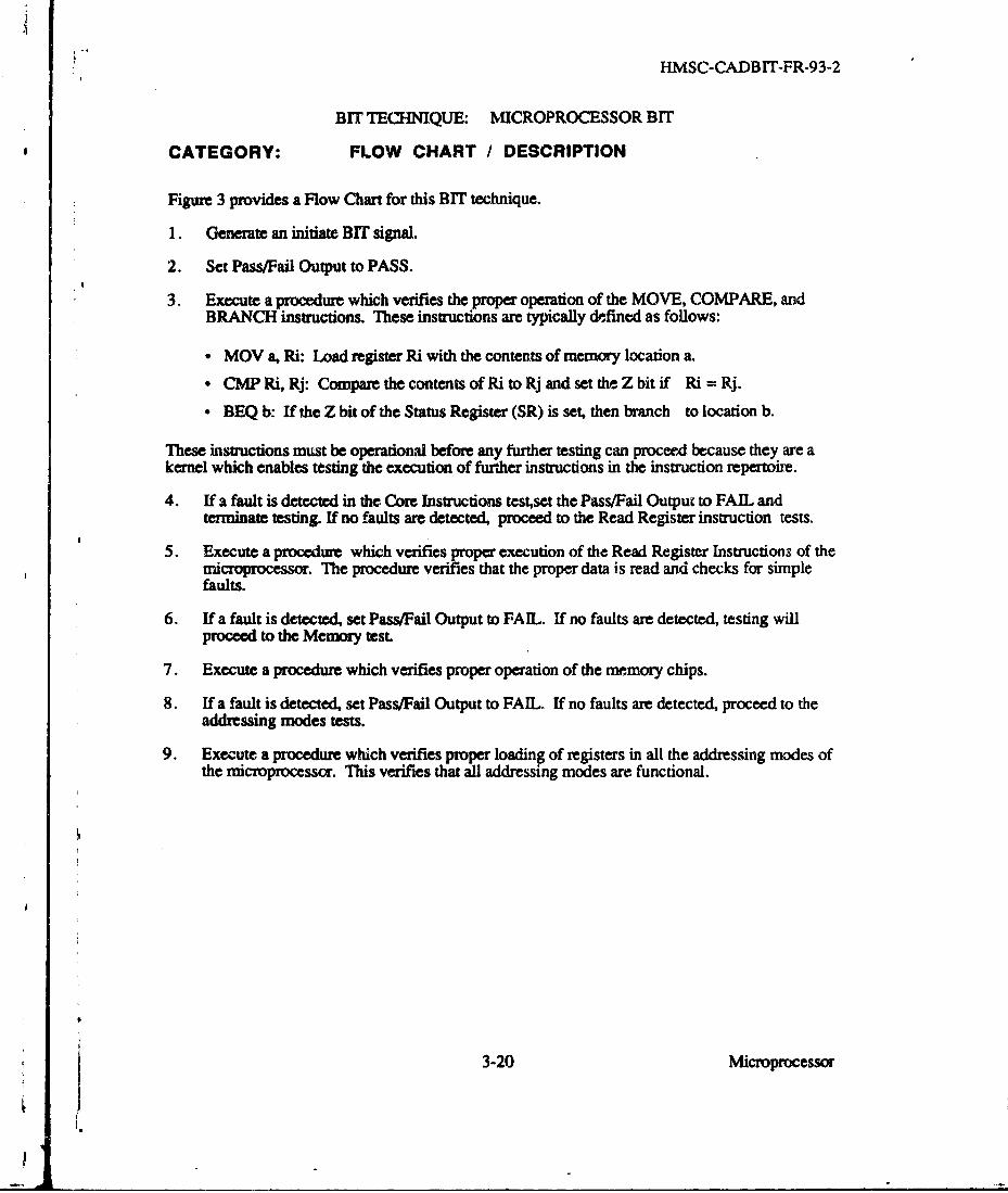
Figure 3 provides a Flow Chart for this BIT technique.
1. Generate an initiate BIT signal.
2. Set Pass/Fail Output to PASS.
3. Execute a procedure which verifies the proper operation of the MOVE, COMPARE, andBRANCH instructions. These instructions are typically defined as follows:
- MOV a, Ri: Load register Ri with the contents of memory location a.
- CMPRi, Rj: Compare the contents of Ri to Rj and set the Z bit if Ri=Rj.
- BEQ b: If the Z bit of the Status Register (SR) is set, then branch to location b.
These instructions must be operational before any further testing can proceed because they are akernel which enables testing the execution of further instructions in the instruction repertoie.
4. If a fault is detected in the Core Instructions testset the Pass/Fail Output to FAIL andterminate testing. If no faults are detected, proceed to the Read Register instruction tests.
5. Execute a procedure which verifies proper execution of the Read Register Instructions of themicroprocessor. The procedure verifies that the proper data is read and checks for simplefaults.
6. If a fault is detected, set Pass/Fail Output to FAIL. If no faults are detected, testing willproceed to the Memory test.
7. Execute a procedure which verifies proper operation of the memory chips.
8. If a fault is detected, set Pass/Fail Output to FAIL. If no faults are detected, proceed to theaddressing modes tests.
9. Execute a procedure which verifies proper loading of registers in all the addressing modes ofthe microprocessor. This verifies that all addressing modes are functional.
3-20 Microprocessor

HMSC-CADBIT-FR-93-2
BIT TECHNIQUE: MICROPROCESSOR BIT
CATEGORY: FLOW CHART DESCRIPTION, Contd
10. If a fault is detected, set Pass/Fail Output to FAIL. If no faults are detected, proceed to theInstruction Execution test.
11. Execute a procedure which verifies that the Instruction Execution process is functional. Thisis accomplished by loading the registers with codewords, executing an Instruction set, andverifying the proper content of the registers.
12. If a fault is detected, set Pass/Fail Output to FAIL. If no faults are detected, proceed to theInstruction Sequence test.
13. Execute a procedure in which all possible ordered pairs of instructions are tested. Orderedpairs of instructions are defined as instructions which are commonly used together. Checkfor the following faults:
" No data dependence (the sequence fault is independent of the operands used with theinstructions).
" Pairwise instruction sequence dependence,14. If a fault is detected, set Pass/Fail Output to FAIL. If no faults are detected, testing will
proceed to the Integrated Controller tests.
15. In general, the fault model for any on-chip peripheral controller is as follows:
* Registers belonging to the peripheral control device have stuck-at faults. The result ofthese faults will be incorrect, or there will be no execution of the device function.
c Faults in decoders of the peripheral control device cause incorrect, or no selection ofperipheral control registers.
0 Faults in the control logic c f the peripheral cause incorrect, or no, execution of thecontroller function.
* A fault in the on-chip periffheral may cause a side effect in other areas of themicroprocessor which nm.y be detected in its readable registers.
16. If a fault is detectedset Pas RFail Output to FAIL. If no faults are detected, theMicroprocessor BIT passed.
3-21 Microprocessor

HMSC-CADBIT-FR-93-2
EXECUTE COREIN/STRUCTIONS
PAS NO SETr PA88nFAJLP• TO FAIL
EXECUTEI ~rI READ REG
SNO SET PASSIFAIL
PAW? [A40=A
TO FAIL
274...44_.1 1
Figure 3 BIT Sequence Flow Chart for Micwopwoccsso BIT (Sheet 1 of 2)
3-22 MicroMssor
*TESTS

HMSC-CADBIT-FR-93-2
NO SET PASS'FAIL
NO• ETPASSAI
TO FAIL
Y YESES
EXECUTE INSTRUCERIP
YTESTS
PASS1SET PASS,'FAIL
EXECUTE INSTRUCTIONSEQUENCETTESTS
YES
274_844_.54
Figure 3 BIT Seqluence Flow Chart for Microprocessor BIT (Sheet 2 of 2)
3-23 Microprocessor

.1
HMSC-CADBIT-FR-93-2
BIT TECHNIQUE: MICROPROCESSOR BIT
CATEGORY: ADVANTAGES
Microprocessor BIT technique provides the following advantages to the circuit designer
1. The real estate penalty will be minimal, basically requiring Read Only Memory (ROM)locations which may already be available if there is spare ROM space after the design iscomplete. If an external test module is required, the real estate penalty will be slightlyincreased.
2. Most of the tests are executed at the operating speed of microprocessor.
3. Monitoring of test results is carried out by the microprocessor itself.
3-24 Microprocessor

RMSC-CADBrI-FR-93-2
BIT TECHNIQUE: MICROPROCESSOR BIT
CATEGORY: DISADVANTAGES
Microprocessor BIT technique poses the following disadvantages to the circuit designer
1. The test memory requirement can be large, aud is dependent on the following factors:
0 Microprocessor characteristics
• Thoroughness of the tests
• Optimization of the test code for fast execution
2. Most of the test code must be wiitten in assembly language or machine code. Assembly andmachine codes are not as readable as high order languages.
f
II
)3-25 Microprocessor

HMSC-CADBrr-FR-93-2
BIT TECHNIQUE: MICROPROCESSOR BIT
CATEGORY: ATTRIBUTES
1. CONCURRENCY
• Concurrent - BIT must be run infrequently during normal operation to maintainconcurrency.
2. TECIhNOLOGY
fDigital
3. CUT MICROPROCESSOR REQUIRED
4. CUT INIERNAL DESIGN REQUIRED?
"• No, unless additional ROM and/or external test module are needed.
5. AREA PENALTY-
"* The number of memory chips needed is proportional to the total memory requirement ofthe self-test program used. If it will not fit in existingmemory, penalty will be accruedconsisting of:
a. Several registers
b. Control logic circuitry
6. WEIGHT PENALTY
- Weight increases as the number of additional memory chips increases.
7. POWER PENALTY
"* Proportional to the number of added memory chips.
"* If an External Test Module and/or memory is required, an additional power penalty will beaccrued.
3.-26 Microprocessor

HMSC-CADBIT-FR-93-2
BIT TECHNIQUE: MICROPROCESSOR BIT
CATEGORY: ATTRIBUTES, Contd
8. TIMING PENALTIES
- Test time is a function of clock frequency and test program length
- Throughput delay is 6 ns.
9. RELIABILITY IMPACT
"• Failure rate increases with the addition of memory chips."* If an External Test Module is required, an additional reliability penalty will be accrued.
10. CONCEPTUAL COMPLJE=
* Circuit design is straightforward.
• Some assembly language programming is required
11. HARDWARE/SOF'rWARE/FRMWARE
"* Some hardware reqired if additional ROM or external test module are required
"• Assembly and/or machine language code are required"* Test software may be either ROM resident or loaded prior to execution
12. DESIGN COST
"* All components used awe readily available at low cost.
"• Software development time of the BIT programs stored in memory increases with thecomplexity and thoroughness of the tests used.
"• Hardware design and debug is minimal.
13. MEMORY REQUIREMENTS
* Proportional to size of test softrare
14. BIT CIRCUITRY SELF-TESTABLE?
*Yes
15. STAND-ALONE (SELF-CONTAINED) BIT?
eYes
3-27 Microprocessor
H1MSC-CADBIT-FR-93-2
BIT TECHNIQUE: MICROPROCESSOR BIT
CATEGORY: DEFAULT DESIGN
This section deseribes the default design for the Microprocessor BIr technique. Refer to Figure 3for the Level H Block Diagram for this BIT technique and Figure 4 for the Default Designschematic.
In many cases, Microprocessor BiT can be accomplished by using the, available ROM to store theBiT software. Additional hardware is needed if either the BIT software will not fit in the existingROM, or if the designer wislhes to test the microprocessor's hardware connections. The externalmicroprocessor pin being tested is an interrupt. Although the interrupt function can be tested usingsoftware, the actual hardware pin function cannot be tested without external stimulus, Figure 4shows how additional ROM can be. added, and a method to test microprocessor inputs.
The additional ROM is shown as U3. It is wired to the microprocessor in the same manner as anyexisting ROM, only mapped to a different location. The 8255A is mapped to the base address8000H by connecting its chip select to the inverted most significant bit of the 16-bit address bus.The outputs of the 8255 drive a 54ALS 157 multiplexer. During normal operation, the existingsystem interrupt is routed through the multiplexer to the P3.2 pin on the microprocessor. Undersoftware control, the 8255 ran use te multiplexer to route an 8255 output to the micropmcessor'sinterrupt input pin (P3.2), thus allowing the BIT software to exercise the port and determine if it isworking properly. After the test, the BIT software would return the configuration to rnormal.
3-28 Nicrprocessor

NOTEs All coone
thr'ough I
U1 _
~16-5-nii- 1U3_1
2725Pg.$ NITIATED'- U
EXISTIG.9.SYpN.I1P~~~ .- P.232Pa. 3 2. 3 sPa .% P . 4 8
gL 70 1 1I' P2 so s
Pa.~P 7 -
as I
I - _______________________ ______________________ ___________________________________________________________ _______as _
Pipi 4,. M rpocso BIT is Defu Des1,i8
~7I PI29pg 3 P3: 2

H-MSC-CADBIT-FR-93-2
NOME All connections to VCC nodsthr~ougk 1K resistor~ pull up
BUSOBUS] (7: .15751 U3 27
PI20.0i 20 JP1.1 P2.1 302 So30M6.2 e 2. 2E0 30
~st P2. so so a
r-P.5 P. 70 70 I
-PG.7 P2.0 -oto3
- P1 P3.26 1
P,. P3.P1. P2.1 'I 1. P3.1 2
- 32 Ft
lLl FILE1YSTAL 31maTV
1"4
-11
Z il l i
L-
LINL.
-___ ___ ___ _- - __ __---_ _ _ - ~ ----- O PRSFIs
Fiiu 42 Mirpocaw BI ekDsg
3-29i3 MicroprocesTsorea~ Deig

HMSC-CADBrT-FR-93-2
BIT TECHNIQUE: MICROPROCESSOR BIT
CATEGORY: BIT TECHNIQUE INSERTION DIAGRAM
Refer to Figure 5 for the BIT Technique Insertion Diagram.
1. Test Program Memmy
If additional ROM is required, connect the data, address, and enable lines of the 47256 ROMto the CUT data, address, and memory chip decoder circuit.
2. External Test Module
If an external test module is required, insert the 8255A using the CUT I/O port decoder logic.Determine which external stimulus (i.e., interrupt, I/O port) lines need to be tested. Connectthe 54ALS 157 multiplexer Y output(s) to the microprocessor input(s) to be tested. Connectthe multiplexer A input(s) to the existing stimulus signal(s).
3-31 Microprocessor
'1

HMSC-CADBrT-FR-93-2
Nc x
3-2Na.orcso

HMSC-CADBIT-FR-93-2
BIT TECHNIQUE: MICROPROCESSOR BIT
CATEGORY: VARIABLE DEFINITIONS
Variable Variable Definition Units
vi. #Bytes for Microprocessor BIT S/W in add'l ROM bytes
v2. Data bus width bytes
v3. #Peripheral functions to test functions
v4. Microprocessor execution speed instructions/sec
v5. #Dynamic instructions for Microprocessor BIT S/W instructions
CATEGORY: COMPONENT DETERMINATION EQUATIONS
The number of units (as represented by CAD symbols) and component parts (physical packages)required to implement the Default Design are calculated as follows:
BIT Technique Parts Table (for Default Design)
Index, i Part Number Part Type Units Required, uiI 54ALS0B IVERTER T2 54ALS157 SELECTOR/MUX ceil ( v3 / b)3 27C256-12 PROM ceil ( 8v2 / b) * ceil((vl/v2)/m)4 8255A PERIPHERAL I/F ceil (v3 / b)
The number of Component Parts Required is calculated (for i-th part) as follows:
ni = ceil ( ui / uppi)
Explanation of symbols used:
ni = Number of components (physical packages) required for i-th partui = Number of units (CAD symbols) required for i-th partuppi = Number of units/package for i-th part (from Table 4.0)ceil = Round up to nearest integer (e.g. 5.3 is rounded to 6)b = Number of data bits for part (from Table 4.0)m Number of memory locations for part = 2aa = Number of address bits for part (from Table 4.0)Vi User-supplied value for i-th variable (see Variable Definitions)
3-33 Microprocessor

HMSC-CADBIT-FR-93-2
BIT TECHNIQUE: MICROPROCESSOR BIT
CATEGORY: PENALTY EQUATIONS
AREA (sq.in.) = Sum ( ni * ai ) + 15% for traces
WEIGHT (gins) = Sum ( ni * wi ) + 10% for solder
POWER (mW) = Sum (ni * pi)
TEST TIME (ns) 0 (This technique has been classified as Concurrent)
DELAY (ns) = 6
Explanation of Symbols Used.
Sum = Sum over parts in BIT Technique Parts Table (i=l to 4)ni = Number of component packages for i-th part in Parts Table
ni is calculated according to Component Determination Equationsai = Area in sq.in. of i-th part in Pars TablePi = Power dissipation in mW (typical) for i-th part in Parts Tablewi = Weight in grams of i-th part in Parts Tablevi User-supplied value for i-th variable (see Variable Definitions)
CATEGORY: BIBLIOGRAPHY
None required.
3-34 Microprocessor
HMSC-CADBiT-FR-93-2
MICRODIAGNOSTICS
BIT TECHNIQUE DATA PACKAGE
CATEGORY: SHORT DESCRIPTION I DIAGRAMS
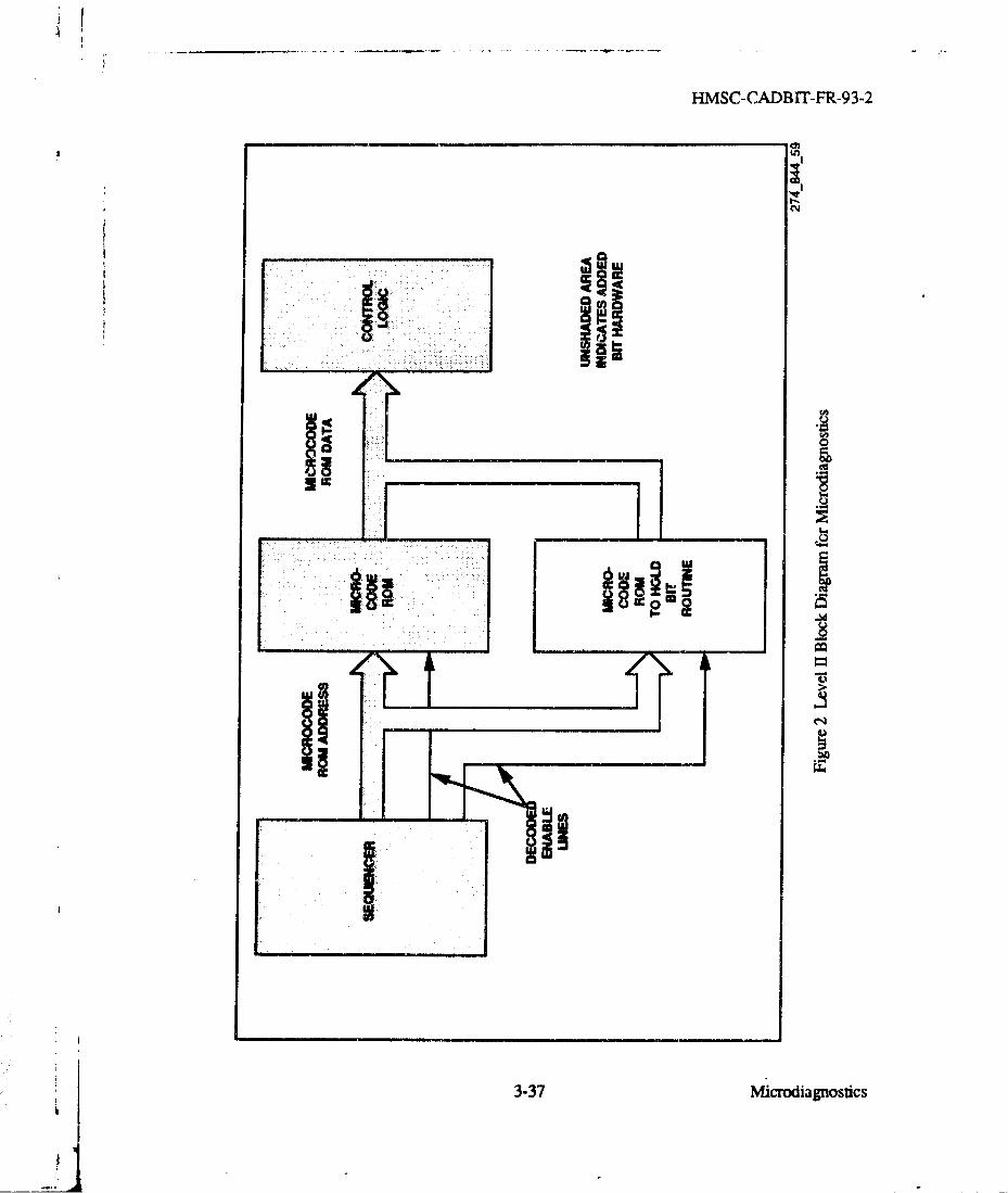
Microdiagnostics is a diagnostic BIT technique that is implemented by microprogramming on amicrocode level. BIT implemented at tie nucrocode level in a microprogramming environmentallows hardware and software testing without the need for a hardware intensive approachcompared to an application software level BIT running out of RAM or ROM.
The technique involves partitioning an area of the microcode ROM to support a small BIT routinewhich is executed by a macro instruction. For the purposes of this document, the macroinstructionwill be called RUNBIT, When the opcode for RUNBIT is encountered, the sequencer will vectorto the specified address of the RUNBIT routine.
The RUNBIT routine would verify operation of the processor circuitry by testing all of itselements. The register stack and all internal Random Access Memory (RAM) can be exhaustivelychecked. A checksum can be generated for microcode ROM and compared with a previouslystored value. All Arithmetic & Logic Unit (ALU) functions can be checked along with theassociated flags and status bits. Data can be routed along all points of the internal buses to verifyoperation of the multiplexing circuitry. RUNBIT could either be run as a subroutine, that is, allstatus and contents of registers placed on stack before execution and restored after BIT iscompleted, or it could be a destructive procedure which initializes the processor after completion.For the purposes of the Microdiagnostics BIT description, RUNBIT is assumed to be non-destruc-tive.
Figures I and 2 show the Level I and 1 Block Diagrams for this BIT technique
3-35 Microdiagnostics

HMSC-CADBrT-IFR-93-2
IL-
j I
0I 0I0
00 W
II
0 0
10?
0 0
3-3 _________ -tic
HMSC-.CADBrT-FR-93-2
OM
iz
3-37 Micrrxliagnostics

HMSC-CADBIT-FR-93-2
BIT TECHNIQUE: MICRODIAGNOSTICS
CATEGORY: FLOW CHART DESCRIPTION
Refer to Figmu 3 for a Flow Chart of this BIT technique.
1. Macro instruction "RUNBIT" is called to initiate testing.
* Save processor status.
- Perform checksum of all microprogram memory.* Step "ALU" through all functions. Check status and flag bits.
* Walk a one through register banks.
- Perform software interrupt test.
- Walk various data patterns along internal bus and check system multiplexing paths.
• Perform selected functional tests of peripheral devices.
2. If all tests pass, restore processor status.
3. If test fails, write status word to board output port to indicate the failure code and, as anoption, halt the processor based on detected fault severity. The result can then be read fromthe Line Replaceable Module (LRM) by the rest of the system.
3-38 Microdiagnostics

HMSC-CADBrr-FR-93-2
SAVE CURRENT CPU
STATUS
ii
PERFORM CHECKSUM OFALL MICROPROGRAM
MEMORY ,
STEP ALU THROUGH ALL ALUFUNCTIONS AND CHECK STATUS
& FLAG SITS . ..
SWALK A ONE THROUGHREGISTER BANK_ f,
PERFORM SOFTWAREINTERRUPT TO TEST
INTERRUPT HARDWARE
WALK A BYTE OF DATAALONG INTERNAL BUS &
CHECK MULTIPLEXING
SPERFORM SELECTED
PERIPHEP..AL CHIPFUNCTIONAL TESTS
NO WRITE V ATUS WORD
NTO BOARD OUTPUT"/PASS? PONT TO INDICA5TEORD
FAILURE AND CODESYES
RESTORE RTA;U8 FAA ES HLOF MEMORYER PROCSSOR
I~mmmsmmm~mm~mNO
END
274_"8458Fiuwr 3 BIT Sequence Flow Cutrn for Microdiagnostics
3-39 Microdiagnostics
HMSC-.CADBf'l-FR-93-2
BIT TECHNIQUE: MICRODIAGNOSTICS
CATEGORY: ADVANTAGES
i. No application software overhead due te microcoded BIT progam.
2. BFr wiUl run faster beeuse it will execute at a mnicroinstrucmtic level
3. Micwprocessor BIT can check internal microcomputer circuitry as well a• peripheral chipfunctions.
CATEGORY: DISADVANTAGES
I. Possible Ipge hardwyre requirement due to size of micracode pgram wemcmry needed tohandle BIT test. E, xample: Larkt BIT slice confiurazions with limited memory.
2. Adequate iemory wAy not be available to run all desired tests if the micmcodc ROM cannotbe expanded.
3 Potwtia1 major k ipact to CU r if at least one spare opcode is rnot available to implernent BITmicroccde,
3-40 Microdiagnoetics

HMSC-CADBIT FR-93-2
BIT TECHNIQUE: MICRODIAGNOSTICS
CATEGORY: ATTRIBUTES
1. CONCURRENCY
* Concurrent - BIT must be called infrequently during application software execution.
2. TECHNOLOGY
. Typical application is digital circuitry.
* Applicable to micro-progammable digital processurs.
- If additional merocry is needed, the samn rnicr-pwgkrn memory devices are used forBIT program as are used in the base design.
3. CUT MICROPROCESSOR REQUIRED?
* Yes. An existing ni'ro-prograrnmable processor is utilized to test itseif and 3ssociatedperipheral devices.
4. CUT INTERNAL DESIGN REQUIRED?
"* No, unless an additional ROM is required.
"* BIT microcode is internal to the CUT. Internal hardw= design is limited to addinf,
nicrocode ROM, if required.
5. AREA PENALTY
* None as long as ,ninoy space is available for BIT aficrocode.. If mcmory is notavailable, microcode ROMs wiP. hav#, to be added pr%"Wpotioala to the size of the BITmicrocode.
6. WEIGHT PENALTY
* Proportional to the area penalty.
3-41 M4icrodiagnostics
il

! ~HMSC-(CY. DP IT-FR-93 -2
BIT TECHNIQUC" MICROMIArWOSTICS
CArEGORY: ATT91BUTIES, Corld
7. POWFR PEINALTY
"* N- poevr p(rnalty if additional ROM is not nevied.,
"* Power penalty is z function of tho h.umber and type of need& ROM chips.
" Power penaitj may be minimized through use of ROMs wih a power-down mode.
8. TIMING PENALTY
" Tast Time - Very fast comptrnd to applic.,tdon code BIT impkwnentation. Approximateexecution trme - (number of BIT micrm-instructions) x (average awcro-iructionexecution time).
"r Thoughput - Throaghpu'm impact is proportiondl to rhe frmquency that eie BIT mayro-mistraction is caUkd.
9. RELLABIlITY hMlPACTr
* Failure rate increases as tho. number of additionli ROM chips increases.
10. CONCEPtIAL COMPLEXIY
* Str~ightforw~ird
11. HARDWARE / SOFTWARE! FIRMWARE
* hardware - Possible adItional microcode ROM(s)
• Software -. Addition of BIT mac-inostuction ca2I ii application code along with a test forfalure and a conditional tmnch statement.
• Firmware-- Test patterns and instrucdons ir microcode
3-42 Micrcdiagnostics

HMSC-CADBlT-FR-93 2
BIT TECHNIQUE: MICRODWAGNOSTICS
CATEGORY: ArTRIBUTES, Conmd
12. DESIGN COST
• Ha•idwr -- No new design beyond the addition of additional ruemor) device(s) ifnecessm-y.
- Software.- Minimal (execute single aii.,xocode instruction lianvs)
• Firmware - Dependent on complexity of BIT sequence but will typically be less comptextian a software implementation,
13. MEMORY REQUIREMENT
* A function of BIT sequncc complexity (micrcode itstructions and test pattens).
14. BIT CIRCUITIY SELF-TESTABLE?
• YES - BiT ,akavoc ROM will be checksummed iong with the CUT microcode.
15. STAND-ALONE (SELF-CONTAINED) BITt
- YES - BIT microco4e is contained in ýhc ptrc.essor nricrucode IXOM. The only pAossible.external =cop ent is the application code call to dte BfI r acr• inst'uction.
16. NOTES
• Mirooxxied BIT technique is contingent on the availability oi at leasc one microcodeinstruction opcode. If an opeode is Po' available, then e, much more complex change to theCUT processor will be required.
1-43 Microdiagnostics
_ i"

, HMSC-CADBJT-FR-93-2
BIT TECHNIQUE: MICRODIAGINOSTICS
CATEGORY: DEFAULT DESIGN
Refer to Figtre 2 for the Level 1I Block Diairau for this BIT technique. No default designschematic hs been included as pan of the ucroxlldagnostics BIT technique. Each application of a
iprocesso design will be unique. The ouly addition to a design needed to implementMicruiagnostics is one or more microcode ROMs of the same type that are already being used inthe design.
3-44 Microdiagnostics

3
HMSC-CADBIT-FR-93-2
BIT TECHNIQUE: MICRODIAGNOSTICS
CATEGORY: BIT TECHNIQUE INSERTION DIAGRAM
Figure 4 shows the BIT Technique Insertion Diagram for this BIT technique.
1. Connect the BIT microcode ROM address lines in parallel with the existing microcode ROMaddress lines.
2. Connect the BIT microcode ROM data lines in parallel with the existing microcode ROM datalines.
3. Connect the appropriate chip enable decoder output to the enable pin of the BIT microcodeROM.
3-45 Microdiagnostics
LA i ;

HMSC-CADB IT-FR-93-2
3-M6 Mkcodiagnostics

HMSC-CADBIT-1R-93-2
BIT TECHNIQUE: MICRODIAGNOSTICS
CATEGORY: VARIABLE DEFINITIONS
Variable Variable Definition Units
v1. #Additional ROMs required for Microdiagnostics BIT #ROMs
v2. Microdiagnostic BIT execution time sec
CATEGORY: COMPONENT DETERMINATION EQUATIONS
The number of units (as represented by CAD symbols) and component parts (physical packages)
required to implement the Default Design are calculated as follows:
BIT Technique Parts Table (for Default Design)
Index, i Part Number Part Type Units Required, ul
27C259-12 .. In= . v
The number of Component Parts Required is calculated (for i-th part) as follows:
ni = ceil ( ui / uppi)
Explanation of symbols used:
ni = Number of components (physical packages) required for i-th partui = Number of units (CAD symbols) required for i-th partuppi Number of units/package for i-th part (from Table 4.0)ceil Round up to nearest integer (e.g. 5.3 is rounded to 6)vi = User-supplied value for i-th variable (see Variable Definitions)
3-47 Microdiagnosucs

HMSC-CADBIT-FR-93-2
BIT TECHNIQUE: MICRODIAGNOSTICS
CATEGORY: PENALTY EQUATIONS
AREA (sq.in.) - Sum ( ni ' aj) + 15% for taces
WEIGHT (irns) Sum (ni * wi ) + 10% for soder
POWER (mW) = Sum (ni *pi)
TEST TIME (sec) v2
DELAY (ns) = 0
Explanation of Symbois Used.
Sum = Sum over pans in BIT Technique Parts Table (i=1 to 1), = Number of component packages for i-th part in Parts Table
ni is calculated according to Component Determination Equationsai Area in sq.in. of i-th part ýn Parts Tablepi = Power disipation in mW (typical) for i-th part in Parts Tablewi = Weight in grms of i-th part in Parts Tablevi User-supplied vnlue for i-th variable (see Variable Definitions)
CATEGORY: BIBLIOGRAPHY
1. T. Sidhar and IP. IAyes, "Testing bit-sliced Microprocessors" in Proc. 9th !nt. Conf.
Fault-Tolerant Computing. Madison, WI: IEEE Comp. Soc. June 1979. PP 211-218.
2. The AM2900 Family Databook, Advanced Micro Devices, Sunnyvale, CA., 1976.
3. D.P. Fulghum, "Automatic Self-Test of a Microprocessor System", Proc. Autotestcon 1976,Arlington, Texas, Nov. 1976. PP 47-52 (Abstracts in IEEE Trans, Aerospace andElectronic Systems, Vol. AES-13 No. 2, March 1977).
3-48 Microdiagnostics

,HMSC-CADBIT-FR-93-2
ON-BOARD INTEGRATIONOF VLSI CHIP BIT
(OBIVCB)
BIT TECHNIQUE DATA PACKAGE
CATEGORY: SHORT DESCRIPTION / DIAGRAMS
OBIVCB makes use of Built-In-Self-Test (BIST) internal to integrated circuits (ICs) resident onthe circuit board. It does this by providing a 'Test Processor Node" on the board, which is capableof addressing a variety of chip Built-In-Test approaches. For instance, the Test Processor Nodecan supply test pattern and collect test data for the ICs which contain internal SCAN/SETcircuitry. Additionally it can also test chips which contain BILBO circuitry.
In general, the Test Processor Node will coordinate chip self-testing, allow for parallel testing, andtake advantage of the more current techniques of self-test.
Types of BIT supported by OBIVCB:
* Scan path techniques
- Internally supported scan, boundary scan, test bus IEEE Std 1149.1 - 1990, i.e.pseudorandom pattern generation and signature analysis is provided on chip.
* Visibility block approach: Built In Logic Block Observer (BILBO), shadow registers,configurable test points, etc.
* Conventional BIST with chip fail or status flags.
* Watchdog timr BIT technique
Figures 1 shows the Level I Block Diagram for this BIT technique, Level 1T Block Diagrams are
provided in Figures 2-4 as follows:
Figure 2 - Level II Block Diagram - Test Processor Node
Figure 3 - Level El Block Diagram - VLSI/VHSIC CUTwith BILBO
Figure 4 - Level II Block Diagram - VLSINVHSIC CUT with SCAN/SET
3-49 OBIVCB
HMSC-CADBrT-FR-93-2
0
3R5 0~VC

HMSC-CADB1T-FR-93-2
cmJ
--------------- ------------------
SI InI
Fl
I c
4 r
I log
Nil
_3-1 OBIVCB

HMSC-CADBrT-FR-93-2
(%m
0
Cd
3-52 BIVC

HMSC-CADB 1T-FR-93-2
r-Z
FAA
ccA
iiz
II
lu0
diS
3-53 ~rV M

HMSC-CADBIT-FR-93-2
BIT TECHNIQUE: OB'-VCB
CATEGORY: FLOW CHART / DESCRIPTION
Figure 5 shows the Flow Chait for this BJT technique.
1. BIT is initiated externally by the 'BiT INITIATE' pulse. A reset pulse is sent to all chips thatcan be initialized, as well as intwupting the processor to vector it to a self-test routine. ThePASS/FAIL indicator is set to PASS.
2. The Test Processing Node performs a self test. This includes a complete test of all registers.read/write memory, as weUl as checksum tests on all program memory. The EEPROM is nottested due to limited write cycle life limitations.
3. If the Test Processing Node does not pass dte self test, the PASS/F.AIL indicator is set toFAIL and the testing process is ended. The CUT registers are left in the transparent (flow-thru) mode. If the Test Processing Node passes the self test, the testing ccrtinues.
4. Upon successful completion of Step 3, &.e processor reads a configuration block in memorywhich tells it:
"* Which and how many SCAN/SET (S/S) and BILBO registers need to be initialized.
"• Which test loops should be assigned to which registers.
"* Which BILBO registers to place in pattern generation, signature, or scan mode.
"* What patterns to place in SCAN/SET registers
"* What "seeds" to place in BILBO registersp
5. The Test Processor Node selects the first test loop and disables the system clock to all CLTs.
6. If the test loop is implemented with CUTs containing BILBO registers, the following testpiocess continues with Step 7 below. If the test loop is implerrented with CUTs containingSCAN/SET registers, the program continues with the SCAN/SET tests in Step 12 below.
7. Seed values are scanned into the BILBO registers.
8. The BILBO registers arc placed in the "PRPIV/MISR" mode and the CUT is clocked 2AN 1times, where "N" is the number of BILBO shift register stages.
3-54 OBIVCB

'I
HMC-CAk)Bfr-FR-93-2
BIT TECHNIQIJE: OBIVCB
CATEGORY: FLOW CHART I DESCHIPT)ON, Contd
9. The BILDO registers are placed in the "SCAN" mode and the signature values are scannedfrom the COT wo the Test Processor Node.
Mt. The signature values are comnpared with k3own good test data stored in EEPROM. If thecomparison data does not agree with the known gcod values, the data is stored in EEPROMand the PASS/FAIL indicator is sem to FAIL. If thie comparison dcpta agrees with the knowngood values, the PASS/FAIL indicator remains at PASS.
11. If all w tioops have not beer. zested, the loop seciuencer multiplemer is set to the next path andthe test prgrm brnwhes control back to Step o'indicated above. Otherwise, the programbrancht4 to Step 16 below.
SC'AN/SET Tests:
12. If the CUT SCAN/SET register is to te "SET" to a given pattern, the SCAN/SET regisver isplaced in the "SET" mnde, a test pateut 4 scanned into the CUT, sufficient time is allowedfor logir. states to settle, and &,- registers are pl2ced in the "SCAN" mode to retrieve theresults. Otherwise, if the m-gis'ar is only scanned, it is loaded with the current results, placedinto "SCAN" mode, and the current results arc retrieved from the register.
13. The scanned results are compared with known good test data in EEPROM. ff thecomparisou data does riot agree with known good values, the data is stored in EEPROM fndthe PASS/FAIL indicator is set to FAIL If the comparison data agrees with the known goodvalues, the PASS/FAIL indicator remains at PASS.
14. If all the required test pwttns have not been applied, the next test pattern is selected and thetest program continves with Step 12 above. Otherwise, the test process continues wit'i Step0S b, low.
CheckTest ultu:
15. If all of the test lcoops have not been tested, the loop sequencer is set to the next path and thetest program branches control b&;k to Step 6 indicated above. Otherwise, the test process•.ontinutas with Scp 16 below.
16 All regi&st-i arepolaced in tfo transparent (flow thn) mode, aLl control lines are placed in thenormal operations mode, and the system clock is returned to the CT IT clock inputs. Testingis 'omplete.
3-55 OBIVCB

HMsc-cADor-FR-93-2
('.1IOSN@LUSU"A HTOIUM.
mumem vs ANS Ws TUr
m Nm
0616E RSOIU Val flMUPANUN7p'LOWINN ODE AM D AU. TONh
TOT SS NNAL OFUNARWS MOOS
IWIOWLO
Fiur BI SquNceFow Chart Fr OBIVC
3-56 V4JMJ

HMSC-CA DBIT-F-93-2
BIT TECHNIQUE: OBIVCB
CATEGORY: ADVANITAG ES
1. In kfning r Test Pmxixessor Node aM,1tcq.;,- a nr.,r hi'war, interface as i•',idlcd tthatcaA bW used for widely vpryn•,,'s ; s of Pip BIT. t . satWx be put into agat array or standard cell so tha Vlemenr tion •n in ns simpla ut its 0 6•r ilechip.
2. Becwt-, at dedicated proce.wssor is uwed, h. is €tntsihle amid c3ýyv tnmfifoid hy reviringfirmwxre.
3. Lhw'r Feedback Shift Register (LFSR, tLcory, the biv3 o; • patti- gvneraIosisgnarreanalysis, is well estamblished, docruwnw4 and prwen. Ir I.h1 i Wault detection hasbeen the subject of swvewl paplr.
4. In tying together various chip BITs with a a.nglo Promzsee Node, 8 hieranical teit struc ,,is built which is w-l deruml and maintainable. This idea cai, b extendud frow tdi card tothe box. and sy,",em lve.Js.
S. A hardware/software W.lwce is w~hieved, aPowing timn costs and chip costs to be workedinto project budgets rmomr e.sily than an app:rrach which is implcmented sole!y in ha.Wviwvieor software.
CATErOiRY: DISADVANTAGES
1. ThIs appiwch requires the CUT to be- largely self testing; that is, it assumen, that BIT isincluded in mrst of the claps, especially VLSI and VHSIC devices.
2. A Processor 'res. Node is requifi, while -not comprising an unreasonablc almount ofhardware for testing a bcwrd of complex logic, may be ovxkiil if the logic is alreadyaccessible and rot partikvarly complex. Each application has to be evaluated separately onthe basis of n.eed.
3. Tne test hardware has been optimized for s'.an path and BILBO type testing. While it canhandk" oth,-r approaches as well, it tenus to conwvtrain circuit design, both on the board levelas well as the clhp level, to this type (.f structure.
4. It requires conrol of system clock.
3-57 OBIVCB

HMSC.CADBIT-FR -93-2
BIT TECHNIqUE: OBIVCB
CATEGORY: ATTRIBUTES
1. CONCURRENCY
* Test is .n-con~wwwent with oofrational use.
2. TECLINOLOGY
•Digimi
3. CUT MICROPROCESSOR REQUIRED?
•No.
4. CUT INTERNAL DESIGN REQUIRED?
• Yes. CUTs require either BILHO or SCAN/SET registers and supporting control logic.
5. AREA PENALTY
The area penalty is defined by the base configuration of the Test Processor Node. Actualarea for the base configuration is given for Dual-In-Line Packages (DIPs). The BILBOand SCAN/SET area penalties awe not pixovided since they are implemented in the CUTVLSI/VHSIC devices.
6. WEIGHT PENALTY
• Defined by the base configuration of the Test Processor Node. The BILBO andSCAN/SET components are implemented in the CUT VLSINVHSIC devices.
7. POWER PENALTY
* Defined by the base configuration of the Test Processor Node and increases in proportionto the number of BILBO and SCAN/SET registers used.
3-58 OBIVCB

HMSC-CADBIT-FR-93-2
BIT TECHNIQUE: OBIVCB
CATEGORY: ATTRIBUTES, Contd
8. TIMING PENALTY
* Test time - Equal to the sum of the Test Processor Node RAM and EPROM test time plusthe test time required to test the BILBO and/or SCAN/SET circuitry. A maximum of fourtest loops are available that may be any combination of BILBO or SCAN/SETVLSI/VHSIC CUTs.
* Throughput delay
- SCAN/SET - The speed of a CUT containing SCAN/SET registers will be less than onewhich does not contain SCAN/SET registers due the addition of two port inputmultiplexing circuitry to the CUT internal latches. The two port feature allows the CUTinternal latches to parallel load test pattemn data from the SCAN/SET registers.
- BLBO- The speed of a CUT containing BILBO registers will be less than one whichdoes not contain BILBO registers due the addition of an input multiplexer in series withthe data lines. The input multiplexer is used to maintain the BILBO(A) input levels at a lowstate during the PRPG/MISR mode.
9. RELIABIITY IPACT
• Failure rate increases due to the added BILBO and/or SCAN/SET registers implemented inthe CUTs and the Test Processor Node control logic.
10. CONC TAL COMPLEXITY
* Moderate to high complexity
11. HARDWARESOFI WARF/FIRMWARE
• Hardware - For the Test Processor Node and added CUT internal BILBO and/orSCAN/SET registers.
* Software - Not applicable.
* Firmware - For the micro-controller EPROM test programming instructions and theexternal EEPROM storage of BIT failure history data.
3-59 OBIVCB

HMSC-CADBIT-FR-93-2
BIT TECHNIQUE: OBIVCB
CATEGORY: ATTRIBUTES, Contd
12. DESIGN COST
• Hardware - Test Processor Node components used are readily available at low cost. TheVLSVVHSIC components require additional registers and logic to implement either theBILBO or SCAN/SET circuitry.
* Software - Not applicable.
* Firmware - The test programming is stored in the micro-controller EPROM.
13. MEMORY REQUIREMENTS
* Microcontroller EPROM memmy storage is necessary for the test sequenceprogmnming. Additional EEPROM memory storage is necessary for seeds, test vectors,and comparison values of test results.
14. BIT CIRCUrTRY SELF-TESTABLE?
* Partially - EPROM and RAM are tested in the micro-controller only. The EEPROM andother supporting BIT circuitry are not self testable.
15. STAND-ALONE (SELF-CONTAINED) BIT?
* No. Supporting BILBO and/or SCAN/SET circuitry are integrated in the VLSI/VHSICcomponents on board.
16. NOTES
" None.
3-60 OBIVCB

SHMSC-CADBIT-FR-93-2
BIT TECHNIQUE: OBIVCB
CATEGORY: DEFAULT DESIGN
Refer to Figures 6-9 for the Default Design schematic. The schematic figures show the followingaspects of the default design:
Figure 6 Test Pro.essor NodeFigure 7 SCAN/SET Implementation within VLSI / VTISIC ChipFigure 8 BILBO Implementation within VLSI / VHSIC ChipFigure 9 BILBO Register Detail Logic
TEST PROCESSOR NODE
The Test Processor Node consists of an Intel 8751 micro-controller, an externally mappedEEPROM data memory device, and test loop select and input data multiplexer logic. The TestProcessor Node is capable of controlling up to 4 independent test loops with an extra parallel I/Oport that may be used for testing of off-board logic.
The micro-controller contains a 4 K byte EPROM that is used to store the application software forimplementation of the BIT algorithms. The 16K (or 2K by 8) EEPROM device is reserved forstorage of CUT input test patterns, expected test results, and BIT failure history data. The upperthree bits of the EEPROM addrss lines are used as page control lines. (8 pages of 256 bytes each)and are connected to the upper address port pins P2.0, P2.1, and P2.2. Port P2.7 is dedicated fora PASS/FAIL output and port P3.2 (_INTO) is used for the 'BIT INITIATE' command input. Theremaining pins of port 2 and 3 arm utilized as data I/O and control lines for the test loops.
When instructed by firmware, the P3.0 (RXD) and P3.1 (TXD) ports are reconfigured fromselectable port latches to a serial interface port ("mode 0"). The serial mode allows the TestProcessor Node to scan data both into and out of the CUTS via the test loops. The serial porttransmits the data in 8 bit increments at a rate of 1/12 of the 8751 clock (12 MHz/ 12 = 1 MHz).Port pin P3.0 is used as a bidir-.ctional data line (DATAJ/O) and P3.1 is used for the serial clock(R/WCLOCK). The DATA-1/O (SCAN-IN) line is used for both the reading and writing of datato the BILBO and/or SCAN/SET registers. The R/W_CLOCK will output a clock cycle for everyserial bit written or read from te DATAI/O (SCANJN) line by the Test Processor Node.
3-61 OBIVCB

HMSC-CADBlT-FR-93-2
BIT TECHNIQUE: OBIVCB
CATEGORY: DEFAULT DESIGN, Contd
JEST PROCESSOQ NODE- Coui
When the Test Processor Node writes data to the CUT (SCAN_IN), the receiving data linemultiplexer (US) output is tri-stated ("floats") so that data from port P3.0 pin may be seriallyshifted into the CUT. When the Test Processor Node reads data frow the CUT (SCANOUT-n),the receiving data line multiplexer (US) output is enabled so that data from the CUT may be seriallyshifted into the P3.0 pin.
The P3.1 (TXD) port is also used as a selectable port latch during BILBO MISR/PRPG clockingoperations to "manually" perform clocking operations that the serial port "mode 0" function cannotperform. PRPG/MISR requires (2AN)- I clock cycles where "N" equbls the number of BILBOshift register stages Since the serial port R/WCLOCK can only transmit in increments of eight (8)clock cycles, the remaining clock cycles are performed by detailed firmware instructions thatalternately write 'I 's and '0s to the port. The BILBO VLSI CUT receives the output port levelchanges and is clocked during the edge transitions of the resulting R/W_.CLOCK output.
As an example, the BELBO CUT detailed in figure 8 contains 8 shift register stages (N=8) and therequired clock cycles for (2AN)- I equals 255. The R/WCLOCK generates 248 clock cycles as 31bytes are written out of the serial port. Seven (7) additional clock cycles are required to completethe 255 clock cycles needed. Therefore, the R/WCLOCK port is reconfigured as a port latch andthe remaining 7 clock cycles are generated by writing discrete'l's and '0's to the R/W clock port.
The function of the Test Processor Node during tests of the BILBO and SCAN/SET test loops willbe discussed in the following sections.
NOTES:"BILBO" = Built In Logic Block Observer"PRPG" = Pseudorandom Pattern Generation"MISR." - Multiple Input Signature Register.
3-62 OBIVCB
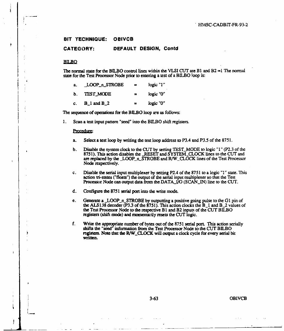
HMSC-CADBiT-FR-93-2
BIT TECHNIQUE: OBIVCB
CATEGORY: DEFAULT DESIGN, Contd
The normal state for the BILBO control lines within the VLSI CUT are B1 and B2 =1 The normalstate for the Test Processor Node prior to entering a test of a BILBO loop is:
a. .LOOP_n_STROBE = logic "1"
b. TESTMODE = logic "0"
c. B-1 and B-2 = logic "0"
The sequence of operations for the BILBO loop are as follows:
1. Scan a test input pattern "seed" into the BILBO shift registers.
a. Select a test loop by writing the test loop address to P3.4 and P3.5 of the 8751.
b. Disable the system clock to the CUT by setting TESTMODE to logic "1" (P2.3 of the8751). This action disables the _RESET and SYSTEMCLOCK lines to the CUT andare replaced by the _LOOP_n_STROBE and R/W_CLOCK lines of the Test ProcessorNode respectively.
c. Disable the serial input multiplexer by setting P2.4 of the 8751 to a logic "1" state. Thisaction wi-states ("floats") the output of the serial input multiplexer so that the TestProcessor Node can output data from the DATA-1/O (SCAN_IN) line to the CUT.
d. Configure the 8751 serial port into the write mode.
e. Generate a _LOOPjnSTROBE by outputting a positive going pulse to the G 1 pin ofthe ALS138 decoder (P3.3 of the 8751). This action clocks the B_1 and B_2 values ofthe Test Processor Node to the respective B 1 and B2 inputs of the CUT BILBOregisters (shift mode) and momenta'ily resets the CUT logic.
f. Write the appropriate number of bytes out of the 8751 serial port. This action seriallyshifts the "seed" information from the Test Processor Node to the CUT BILBOmogisters. Note that the R/WCLOCK will output a clock cycle for every serial bitwritten.
3-63 OBIVCB
----- ----

HMSC-CADBIT-FR-93-2
BIT TECHNIQUE: OBIVCB
CATEGORY: DEFAULT DESIGN, Contd
2. Set the BILBO egister to the "PRPGIMISR" mode and clock the registers (2AN) -1 times (Nis the number of shift registers in the BILBO (A) register).
a. Set BL,1 control line to logic "1" (P2.5 of 8751).
b. Generate a _LOOP.nSTROBE by outputting a positive going palse to the GI pin ofthe ALS138 decoder (P3.3 of the 8751). This action clocks the B-1 and B_2 values ofthe Test Processor Node to the respc,.ive B I and B2 inputs of the CUT BILBOregisters (PRPG/MISR mode) and momentarily resets the CUT logic.
c. The registers are clocked (2AN) - 1 times by writing the appropriate number of bytesout of the 8751 serial port and filling in the remaining clock cycles with theR/WCLOCK port reconfigured as a selectable port latch. For more informationregarding operation of the serial port, please refer to the Default Design Description ofthe Test Processor Node.
3) SCAN the signature data out of the BILBO registers.
a. Set B-1 control line to logic "0" (P2.5 of 8751).
b. Generate a ...L OP_.nSTROBE by outputting a positive going pulse to the G1 pin ofthe ALS138 decoder (P3.3 of the 8751). This action clocks the B_I and B_2 values ofthe Test Processor Node to the respective B I and B2 inputs of the CUT BILBOregisters (shift mode) and momentarily resets the CUT logic.
c. Configure the 8751 serial port into the read mode.
d. Enable the multiplexer tri-state output by setting P2.4 of the 8751 to a "0" state. Thisaction connects the "SCANOUTn" to the selial input DATA-1/O (SCAN-IN) of theTest Processor Node.
e. Perform the appropriate number of read operations (8 bits uer 8751 read instruction.).This action serially shifts the "signature" information from the CUT BILBO registers tothe Test Processor Node. Note that the R/W.CLOCK will output a clock cycle forevery serial bit written.
3-64 OBIVCB

HMSC-CADBIT-FR-93-2
BIT TECHNIQUE: OBIVCB
CATEGORY: DEFAULT DESIGN, Contd
4. Set BILBO register to transparent (flow-dt-u) mode.
EMdure:
a. Set B- I control fine to logic "I ". (P2.5 of the 875 1).
b. Set B-2 control line to logic "I". (P2.5 of the 875 1).
c. Generate a _LOOP-n.STROBE by outputting a positive going pulse to the G I pin ofthe ALS138 decoder (P3.3 of the 8751). This action clocks the BI and B_2 values ofthe Test Processor Node to the respective BI and B2 inputs of the CUT BILBOregisters and momentarily resets the CUT logic.
d. Set B-1 and B_2 control lines to logic "0".
e. Enable the system clock by setting TESTMODE to logic "0" (P2.3 of the 8751).
3-65 OBIVCB

HMSC-CADBIT-FR-93-2
BIT TECHNIQUE: OBIVCB
CATEGORY: DEFAULT DESIGN, Contd
The normal state for the Test Processor Node prior to entering a test of a SCAN/SET loop is:
a. _LOOP_n_STROBE = logic "1"
b. TESTMODE - logic "0"
c. Bl and B_2 - logic "0"
The allowable operations for the SCAN / SET loop are as follows:
1. Scan a test input pattern into the SCAN/SET shift register.
a. Disable the serial input multiplexer by setting P2.4 of the 8751 to a logic "1" state. Thisaction tri-states ("floats") the output of the serial input multiplexer so that the TestProcessor Node can output data from the DATA_ /0 (SCAN_IN) line to the CUT.
b. Configure the 8751 serial port into tie write mode.
c. Write the appropriate number of bytes out of the 8751 serial port (Note that allSCAN/SET loops will be loaded at the same time). This action serially shifts the testpattern from the Test Processor Node to the CUT SCAN/SET registers. Note that theR/W_CLOCK will output a clock cycle for every serial bit written.
2. Scan CUT test data out of the SCAN/SET shift register.
ftodr:
a. Select a test loop via the ALS253 multiplexer by writing the test loop address to P3.4and P3.5 of the 8751. This action selects the output of the CUT "SCANOUT_n" to betested.
b. Configure the 8751 serial port into the read mode.
c. Enable the multiplexer tri-state output by setting P2.4 of the 8751 to a "0" state. Thisaction connects the "SCAN_OUT_n" to the serial input DATA_I/O (SCANIN) of theTest Processor Node.
d. Perform the appropriate number of read operations. This action serially shifts the testdata from the CUTS CAN/SET registers to the Test Processor Node. Note that theR/W_CLOCK will ouiput a clock cycle for every serial bit written.
3-66 OBIVCB

HMSC-CADBIT-FR-93-2
BIT TECHNIQUE: OBIVCB
CATEGORY: DEFAULT DESIGN, Contd
SCAN/SET. Contd
3. Parallel load the shift register with test data from the CUT logic.
a. If desired, disable the system clock to the CUT by setting TESTMODE to logic "I"(P2.3 of 8751).
b. Select a test loop via the ALS253 multiplexer by writing the test loop address to P3.4and P3.5 of the 8751. This action selects the output of the CUT "SCAN_OUT_n" to betested.
C. Set B-1, B_2 control lines to logic 0, 1 respectively (P2.5 , P2.6 of 8751).
d. Generate a _,LOOP_n_STROBE by outputting a positive going pulse to the G I pin ofthe ALS138 decoder (P3.3 of 8751). This action loads the contents of the CUT latchesinto the SCAN/SET shift registers.
4. Parallel load the CUT latches with data from the shift register.
a. If desired, disable the system clock to the CUT by setting TEST_MODE to logic "1"(P2.3 of 8751).
b. Select a test loop via the ALS253 multiplexer by writing the test loop address to P3.4and P3.5 of the 8751. This action selects the output of the CUT "SCANOUTn" to betested.
c. Set B-I, B_2 control line to logic 1, 0 respectively (P2.5, P2.6 of 8751).
d. Generate a _.LOOP_n_STROBE by outputting a positive going pulse to the G I pin ofthe ALS 138 decoder (P3.3 of 8751). This action loads the contents of the SCAN/SETshift register into the CUT latches.
All CUT logic using SCAN/SET loops will be, restored to normal operation when TEST_MODEcontrol line is returned to logic "0" (P2.3 of 8751).
3-67 OBrVCB

H?, SC-CADBITB-FR-93-2
BIT TECHNIQUE: OBIVCB
CATEGORY: DEFAULT DESIGN, Contd
1. All VLSI/VHSIC chips will be disabled from normal operation when testing of any loop is inprogress. The system clock is disabled and replaced with the microprocessor read/writeclock.
2. The parallel test bus has limited capability due to a lack of dedicated addrcss and control datalines.
3. All Test Processor Node read/write clock cycles used to clock the CUT during testing are in 8clock cycle increments.
4. Current implementation lacks a dedicated communication port to report detailed BIT resultsand failure histories.
3-68 OBPICB

We-
1644
at .1.
U1 4
SCAN OUT >----
- T2
7Fgw
0u

-RMSC-CADMIT-FR-93-2
144AL313
31_ _ 241A?_ M
40 40 a
_________ so4
3 vix 1
-j i------.- PARALLEL TEST BLUS('7:O
34$4A4.$* 301
,VA -C> LOOP 2 STROBE...- > LOOP 3-STROBE
-';.- L ....- F I0 ,C
--C> RWCLOCK----- ---- <,, DATA tO (SCAN-IN)
IESTMODE'S
LOOP 0STROE;- --- ___--_BILBO
let ,,.V.- VL S I
Ics
SCAN0OUT 04
1- 1 1,c
--- •._•__lLOOP I S'1OB
.SCANISET
Figim 6 Test Processor Nod& Default Design for OBTVCB
3-69 OBJvCH

-4-11
U-F
U-Cý
C')R
Figur 7 ScazV~et Implemnentation Widiin VLSI C)
3-70

HMSC-CADBrT-FR-93-2
4 4
wWWs
Figue 7Sca~ct nplmenatio WiiinVLSIChi - efaut Dsig
~I3-70ZZ ___V

H-MSC-CADBIT-FR-93-2
I IIX
U5 54LSISTU6 54ALS157
B 2 Cz>- -
Sn _STROBELD'- .1 K> BLBW S
Il y I
I I II KL GI
(SAN OUT 'v4c CU
D ATA II,IU 4
Figme 9 BL.BO bnplcrntanwi Within VLSVIIHSJC Chip - Default Design
3-71 OBIVCB

ZI Z2 Z3 Z4 Z5 Z6
B I -
VISA III IAviol Vill 11OC gto VIGOS vilS lIA UIIIA Vuses III? vUSC
5135 12u c Vile VIA U|gI aUM
€Yee Yee Wcccc
U14 uVISA 11139 VISA Visa U1AV1esAO
U" I IA
SII " S I'A_ 0 o
At TZ - -
:3 13- --<
T4 g3 ot i O
Yet Wee Yee Vcc 9ee Yee
04AL555 112282234AIS
54ALC
QI1 02 03 04 Q5 Q
Fig= 9E

HMSC-CADBIT-FR-93-2
Z 4 Z5 Z6 z7Z 8
afll* VSIA 111?A vies UI?8 VZ4c VSTC DIeS III o UR1Aujec 34ALSOOA
*0 aIS ai*vs
Vce VV et Vcc Vcc
I als VIADo S AU0
CKCLI L L CLK a81 B 8 2 Mode
o 0 Sh f i ing0 1 Re setf
DOE IO or, IOU lox 10I 0 PRPG/MISR
Yce vcc Vcc Vcc Vcc
S4ALSO
ki 4 Q 6 Q 7 Q 8
9 ~~~Figuit 9 BIBO Registr DeMBi Logic - Defa&J Design
3-72 02OB1VCB

HPMSC-CADB1T-FR-93-2
BIT TECHNIQUE: OBIVCB
CATEGORY: BIT TECHNIQUE INSERTION DIAGRAM
Figure 10 shows the BIT Technique Insertion Diagram for this BIT technique.
BTID 1 (Test Processor Node)
1. Coumect the BIT_INITIATE line to the appropriate LRM interfacc pin.
2. Conne( tthe _RESET signal line to the master reset signal on the LRM.
3. Connect PASS_FAIL output sicgnal to the appropriate LRM interface pin.
4. Connect the PARALLEL_TEST_BUS signal lines (8 total) to unused LRM interface pins.The signal originating at 11I pin 8 (P1 7) is the Most Significant Bit (MSB) of the bus.Subsequent connection to these lines (off-board) may be made as a user option.
If any of the 4 test loops of the TEST PROCESSOR NODE are to be used off board thenperform the following additional connection steps.
5. Connect the R/W_CLOCK, DATA-1/O (SCAN_IN), PASS/FAIL, B_1, B_2, and
TESTMODE signal lines to unused LRM interface pins,
6. For each test loop ("n" r- loop number) to be connected off-board:
a. Connect the appropriate _LOOP._n_STROBE signal lines from U4 to unused LRMinte•face pins.
b. Connect the appropriate SCAN_OLUTn signal lines from U5 to unused LRM interfacepins.
1. Connect the BJ, B2, TESTMODE, R/WCLOCK, cuid DATA-1/O (SCANIN) signallines, through unused VLSI device Interface pins, to the appropriate signal interface pins ofthe Test Processor Node (BTID 1).
2. Connect the -RESET and SYSTEMCLOCK signal lines, through VLSI device pins, to theLRM master reset and system clock signals.
3. Connect the appropriate _LOOP_n_STK.OBE signai line, through an unused VLSI deviceinterface pin, to the appropriate LOOPn._STROBE signal line from the 'est ProcessorNode (BTID 1).
4. Connct.• the appropriate SCAN_OUTin signal line, through an unused VLSI device interfacepin to the appropriate SCANOUTn signal line on the Test Processor Node (BTID 1).
3.73 OBIVCB
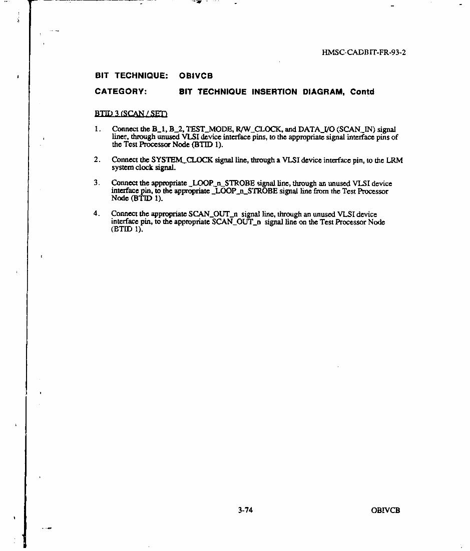
A
I-HMSC-CADBIT-FR-93-2
BIT TECHNIQUE: OBIVCB
CATEGORY: BIT TECHNIQUE INSERTION DIAGRAM, Contd
BTID 3 (SCAN! SET)
1. Connect the B_1, B_2, TESTMODE, R/WCLOCK, and DATA-/O (SCAN-IN) signallines, through unused VLSI device interface pins, to the appropriate signal interface pins ofthe Test Processor Node (BTID 1).
2. Connect the SYSTELMCLOCK signal line, through a VLSI device interface pin, to the LRMsystem clock signal.
3. Connect the appropriate _LOOP_n_STROBE signal line, through an unused VLSI deviceinterface pin, to the appropriate _LOOP_n_STIROBE signal line from the Test ProcessorNode (BTID 1).
4. Connect the appropriate SCANOUT-n signal line, through an unused VLSI deviceinterface pin, to the appropriate SCAN_OUT_n signal line on the Test Processor Node(BTID 1).
3-74 OBIVCB

HMSC-CADBIT-FR-93.2
I
, ,
iI ,
I'I
7--7
3-75 OBIVCB

IIMSC-CADBrI-FR-93-2
BIT TECHNIQUE: OBIVCB
CATEGORY: VARIABLE DEFINITIONS
None required.
CATEGORY: COMPONENT DETERMINATION EQUATIONS
The number of units (as represented by CAD symbols) and component parts (physical packages)
required to implement the Default Design are calculated as follows:
BIT Technique Parts Table (for Default Design)
Index, i Part Number Part Type Units Required, uiT 154AS138 DECODER/DEMUX 12 54ALS253 SELECTOR/MUX 13 54ALS373 LATCH I4 18751H MICROCONTROLLER 15 M55310/18-12 OSCILLATOR I6 2817A-200 BUFFER 17 CMR03 COMPARATOR 28 RNR55 RESISTOR 2
The number of Component Parts Required is calculated (for i-th part) as follows:
ni = ceil ( ui / uppi)
Explanation of symbols used:
ni = Number of components (physical packages) required for i-th partui = Number of units (CAD symbols) required for i-th partuppi = Number of units/package for i-th part (from Table 4.0)ceil = Round up to nearest integer (e.g. 5.3 is rounded to 6)
3-76 OBIVCB

HMSC-CADBIT-FR-93-2
BIT TECHNIQUE: OBIVCB
CATEGORY: PENALTY EQUATIONS
AREA (sq.in.) = Sum ( ni * ai ) + 15% for traces
WEIGHT (gms) = Sum ( ni * wi ) + 10% for solder
POWER (mW) = Sum (ni * pi)
TEST TIME (sec)= tMPBIT + tBILBO + tSCAN + tTERM
DELAY (ns) = 0.0
Explanation of Symbols Used.
Sum = Sum over parts in BIT Technique Parts Table (i=1 to 8)ni = Number of component packages for i-th part in Parts Table
ni is calculated according to Component Determination Equationsai = Area in sq.in. of i-th part in Parts TablePi = Power dissipation in mW (typical) for i-th part in Parts Tablewi = Weight in grams of i-th part in Parts TabletMPBIT = Microprocessor BIT execution time = 0.0347 sectBILBO = BILBO setup time = 0.000012 sectSCAN = SCAN setup time = 0.000012 sectTERM = BIT termination time = 0.0000005 sec
3-77 OBIVCB

HMSC-CADBIT-FR-93-2
BIT TECHNIQUE: OBIVCB
CATEGORY: BIBLIOGRAPHY
1. V.R. Subramanyam, L.R. Stine, (TRW), "Design for Testability for Future Digital AvionicsSystems", IEEE, 1986. Describes a Module Maintenance Node which is the basis for theTest Processor Node in the OBIVCB.
2. R. Frohwerk, "Signature Analysis: A New Digital Field Service Method", Hewlett-Packard,1977. Includes a good tutorial on Linear Feedback Shift Registers.
3. LeBlanc, "LOCST-LSSD On Chip Self Test", iEEE Design & Test of Computers, 1984.
4. D. Bacht, "Understanding Signature Analysis", Electronics Test, Nov. 1982, pg 28.
5. B. Konemann, Joachim Mucha and Gunther Zwiehoff, "Built-in Logic Block Observer",IEEE Test Conference, Cherry Hill, NJ, 1979.
3-78 OBIVCB

H1V1SC-CADW rI-FR-93.-2
BUILT-IN LOGICBLOCK OBSERVER
(BILBO)
BIT TECHNIQUE DATA PACKAGE
CATEGORY: SHORT DESCRIPTION I DIAGRAM
A Built-In Logic Block Observer (BILBO) is a multifunctional circuit which can be configured inany one of the following modes of operation:
1. Latch2. Shift register3. Multiple Input Signature Register (MISR) or Pseudorandcm Pattern Generator (PRPG)4. Reset the BILBO
The configuration is selected by 2 mode control bits. BILBO circuitry can be used to performsignature analysis using a pseudorandom pattern generator (PRPG) and a multiple input signatureregister (MISR) which is an effective method of testing complex digital circuit•y. The foundationof this Built-In-Test (BIT) technique is built on the fact that for a given sequence of stimuli, a fault-free Circuit Under Test (CUT) will output a particular digital stream. Using the data compressiontechniques of signature analysis, an output signature accumulated can be saved in a MISR. At theconclusion of the application of a given set of stimuli, the contents of the MISR are then comparedagainst the known good signature. Initiali2ation of the CUT and the BIT circuitry must be doneprior to the execution of this technique. By utilizing the BILBO circuit, initialization can be easilyachieved using scan-path techniques. The versatility of BILBO allows for the combination of twoBIT techniques-SCAN and PRPG/M1SR. This combination is especially useful when testingcombinational logic stages that are separated by latches. Some of these latches are replaced withBILBO circuits. During normal operation, the BILBO functions as an ondinary latch.
During test initialization, each BILBO is configured as a serial shift register, and an initial seedvalue is shifted into the circuit. The BILBOs are then configured into a PRPG and MISR pairs.This allows for complete testing of the CUT.
Figures 1 and 2 provide Level I and II Block Diagrams for this BIT technique.
3-79 BIZBO
&I

FvIMSC-CADBIT-F-R-93-2
-' - J s
(0
388 j 0 BO

HiMSC-CADBUI-FR-93-.2
0 C4
C2A
3_8__ _ _ _B

HMSC-CADBIT-FR-93-2
BIT TECHINIQUE: BUILT-6I LOGIC BLOCK OBSERVER (BILBO)
CATEGORY: FLOW CHART / DESCRIPTION
Figure 3 shows the Flow Chart for this BIT technique.
1. Circuit Under Test (CUT) is powered up.
2. An initiate BIT signal iz generated. Reset the PASS/FAIL Flip-Flop to PASS.
3. Using the BILBOs as shift registers, an initial seed pattern is scanned into the BILBOregisters.
4. BILBO (a) is configured as A Pseudorandom Pattern Generator (PRPG) and BILBO (b) isconfigured as a Multiple Input Signature Register (MISR).
5, Random testing is perfotmed.
6. BIL20 (b) now contains the CUT signature which is fed into a comparator.
7. If the CUT signature does not match the Good Machine (GM) signature, set the PASS/FAILFlip-Flop to FAIL. If the CUT signature matches the GM signature, the test passed.
8. BILBOs are reconfigured to function as latches.
3-82 BILBO

HMSC-CADBIT-FR-93-2
RESET PASSILEFFRN
I SCAN IN INITAL ISEE s PATTRN.
INTSO 811.90 REGISTERS
CONFIGURE BIL0~ASAPRPG J
I CONGURE BILBo (b) I
LERFRM PSEUDO-RANDOM
NO SETACTUL SINATUE MACHESPASS/FAILGOODMACHNE SGNATREFLIP-FLOP TO FAIL
RIECONFIGURE
BILBO (a) A (b) TOOPERATIONAL I-MODE (LATCH)
274ý_84_67
Figur 3 BIT Sequence Flow Chart For Built-In Logic Block Observer (BILBO) BIT Technique
3-83 BILBO

HMSC-CADBIT-FR-93-2
BIT TECHNIQUE: BUILT-IN LOGIC BLOCK OBSERVER (BILBO)
CATEGORY: ADVANTAGES
BILBO provides the following advantages to the circuit designer:
1. One circuit design can be used for multiple functions, giving the advantages of commonality(custom integrated circuit design can be made and used in many places).
2. The versatility of BILBO allows the designer to combine the advantages of SCAN techniqueswith PRPG/MISR techniques. There is a considerable reduction in test result storageachieved by signature analysis which provides data compaction algorithm.
3. The test data are gathered at the rated internal speed of the integrated circuits. No additionaltest clock is needed. The data sampling and compaction are performed completely inside theCUT.
4. A much higher failure detection rate is achieved when compared to other techniques such astransition counting. This is an efficient and compact tool for monitoring internal test pointson complex digital I.C.s. Loss of fault coverage incurred using signature analysis is 5% for8-15 bit MISRs, 1% for 16-23 bit MISR, and 0% for MISRs of 24 or more BITS (perMIL-STD-885 procedure 5012.1).
5. Minimal software support is required.
CATEGORY: DISADVANTAGES
BILBO provides the following disadvantages to the circuit designer:
1. BILBO must be incorporated as part of the original design of the CUT
2. BILBO modules are more complex than the latches they replace. This results in additionalcircuitry.
3. Limited control of test vector sequencing which is more effective with high amount ofcombinational logic circuitry.
4. Circuit throughput delay will increase sirce BILBO is used as an input or output register.
3-84 BILBO

HMSC-CADBIT-FR-93-2
BIT TECHNIQUE: BUILT-IN LOGIC BLOCK OBSERVER (BILBO)
CATEGORY: ATTRIBUTES
1. CONCURRENCY
• Non-concurrent
2. TECHNOLOGY
•Digivil
3. CUT MICROPROCESSOR REQUIRED?
*No
4. CUT INTERNAL DESIGN REQUIRED?
,Yes
5. AREA PENALTY
* BILBO latches are more complex and take up more area than the conventional latches theyreplace.
- Some test control logic is also required.
* The comparator which compares the good machine signature to the actual signature takesup area.
6. WEIGHT PENALTY
• Proportional to the weight of the test control logic, the additional circuitry of the BILBO
module, and the comparator.
7. POWER PENALTY
* Proportional to the power dissipated by the test control logic, the additional circuitry of theBILBO module, and the comparator.
3-85 BILBO

RHMSC-CADB IT-FR-93-2
BIT TECHNIQUE: BUILT-IN LOGIC BLOCK OBSERVER (BILBO)
CATEGORY: ATTRIBUTES, Contd
8. TvIMING PENALTIES
0 Test time - equal to the number of test patterns divided by the application rate.
* Throughput delay - operational speed is slowed due to the propagation delay through theBILBO cells.
9. RELIABIUTY IMPACT
* Failure rate increase due to Test Control Logic, the BILBO module, and the comparator.
10. CONCEPTUAL COMPLEXITY
* Circuit design is moderate in complexity.
11. HARDWARFSOFTWARE/F1RMWARE
* Hardware
12. DESIGN COST
"* All components used are readily available at low cost.
"* Hardware design and debug is minimal.
13. MEMORY REQUIREMENTS
- Minimal, may be required to store test control routine and seeds.
14. IS BIT CIRCUITRY SELF TESTABLE?
*Yes
15. STAND-ALONE (SELF-CONTAINED) BIT?.
*Yes
16. NOTES
"None
3-86 BILBO

HMSC-CADBIT-FR-93-2
BIT TECHNIQUE: BUILT-IN LOGIC BLOCK OBSERVER (BILBO)
CATEGORY: DEFAULT DESIGN
This section describes the sequence of events for the BILBO BIT technique default design. Referto Figures 4 and 5 for the Default Design srhematic.
1. At the beginning of the test, test TESTINITIATE signal goes low and triggers thefollowing:
a. Presets U1A test control flip-flop and enables TESTCLOCK signal to activatecounters and BILBOs.
b. While the TESTINITIATE signal holds low, the next rising edge of theTEST_CLOCK signal loads zeroes into the synchronous 4-bit binary counters U4, U5,and U6.
c. The _Q of UlA test contra, flip-flop disables U10A, U10B, U10C, U10D, U1I1A,U1 lB, Ul IC, and Ul ID (and gates). This disables the normal inputs to BILBO #1and maintains all zero inputs to BILBO #1 during testing.
d. The _Q of U1A test control flip-flop enables U9 8-bit identity comparator. The Q ofU1A test control flip-flop disables U12A and U12B octal buffers and places the outputsof CUT into high impedance
e. Clears U2A and U2B flip-flops which sets BI = '0' and B2 = '0'. This puts theBILBOs into Scan Mode.
f. Clears the Pass/Fail flip-flop UlB to PASS.
2. After the TlEST_INITIATE signal goes back to high, the TEST_CLOCK signal startsincrementing counters U4, U5, and U6. During the first sixteen clock cycles U5/QA outputsbit sequence 00000000 and 00000001. While in Scan Mode, BILBO #2 scans in 00000000and BILBO #1 scans in 00000001 accordingly.
3. As soon as thte initialization is completed, U2A flip-flop is set by QA of U5 counter tochange BI from '0' to '1' and stays latched to '1' during the testing. B1 = '1' and B2 = '0'puts the CUr into PRPG/M1SR test mode.
3-87 BILBO

HMSC-CADB IT-FR-93-2
BIT TECHNIQUE: BUILT-IN LOGIC BLOCK OBSERVER (BILBO)
CATEGORY: DEFAULT DESIGN, Contd
4. After 255 TESTCLOCK cycles (2A8 - I = 255), U4/RCO and U6/QA are both high andindicates that the end of the PRPG/MISR test mode. These two signals are ended to triggerthe. following:
a. Clears U1A test control flip-flop and disconnects TESTCLOCK signal to counters andBILBOs.
b. Enables U10A< U10B, U10C, U1OD, U1l1A, U 11 B, U11C, and Ul ID (and gates).This allows normal inputs flow to CUr.
c. Disables U9 8-bit identity comparator and enables U12A and U12B octal buffers forthe outputs of the CUT.
d. Presets U2A and U2B flip-flops which sets BI = '' and B2 = '1'. This puts theBILBOs into Latch Mode.
e. Clocks in the result of the comparison of Good Machine Response and test signature.This result is registered by the Pass/Fail flip-flop U1B.
5. The circuit resumes normal operation and it will go into test mode when theTEST_INITIATE signal goes low again.
3-88 BILBO

54ALSOC 6.4 L L306
VIA
U7AL2 54ALS74A
54AISII3
T E ST I NI T IPAT E
34ALS?4A U3A ---- CLID NC
I S~~4ALSOA II
>CLICLI -
-A *ASI as
C C
TEST _CLOCKC>. ______ _____ ___
- - S4ALS04A
USS4ALIII-I
6CLIN
06 V3 USA
34LII 4ALSOD 34AL804
F LIAO NCO
00

Z 2
54ALSOS
S4AL30c; 34L@ 4ALSOI 54ALS00 5 4ALSOO 5A ALSQ9 SM o 4ALSOO 54ALSOs
S4Ap
U4A1 3 54AS I.
54ALI L IOU.1
atgw 4 ILO- ef14 esg
45) 3-89661
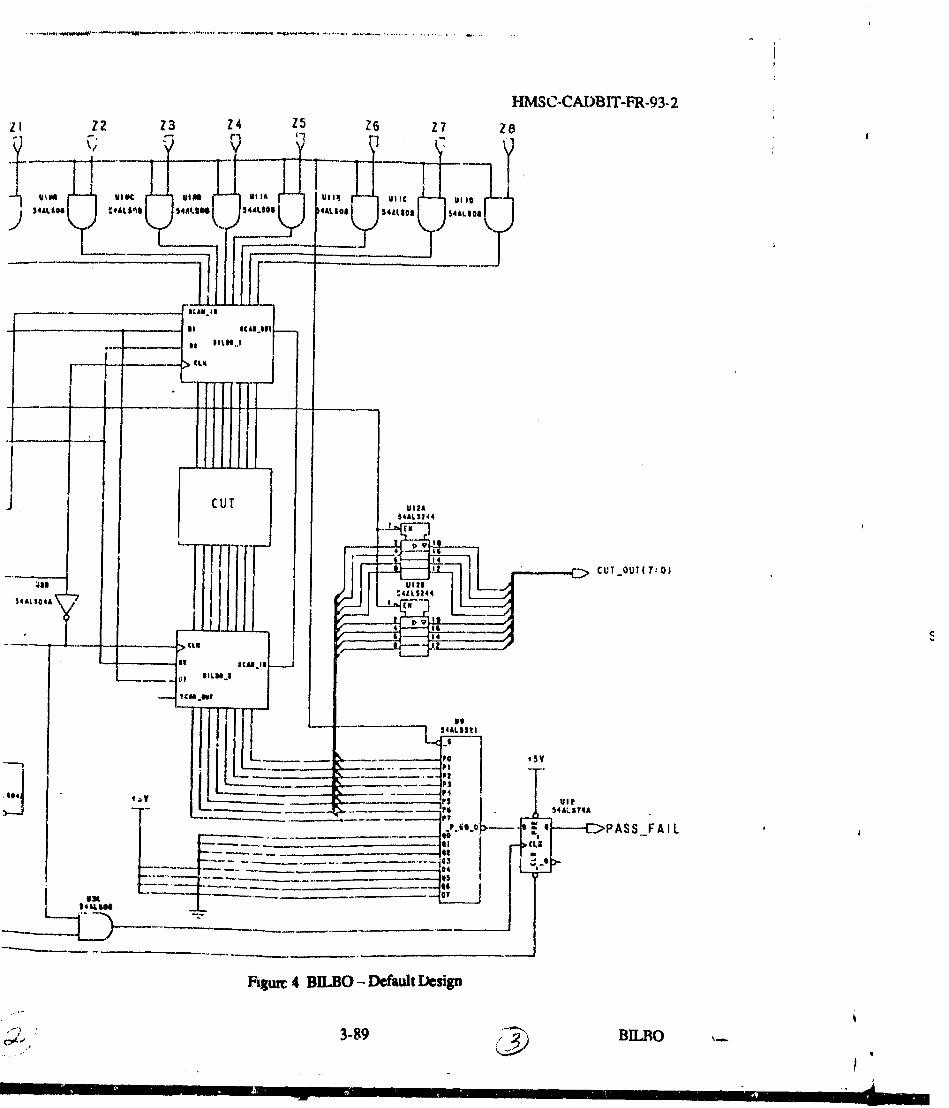
HMSC-CAI)Bf1'-FR-93-2
21 2 Z 3 Z 4 Z5 Z6 2 7 28
91111 v I P VIIM, 91 A W NUitvile
141.0 ) I~L'I 4Aik 34AL111 IM1Sol 54ALIcs 54ALICA
JCUT U25011.31244
L -i
iLli 011 CIOT7:01
4I3034 'aL 0
AL-4 Em. L
j
11
t
LE - of
I- I90
_________goi N - -.1
3-8AS FAILO

zIZ2 Z 3 Z 4 z 5 7 4
WUIOA UIA U108 Villc ulI VIO vii ViO ID Ugh i S UI?A U148 II78 j
Ycc
IIIA. 3At OT2 VISAD UseVIASA
U3A Ih IAVliVS14ALS74A 54AI.ST4A 54ALS?4A A 54AL174A 54ALS74A V~
D. -
46 a
B-A
At ii -SCAN-INL a-
A3 T3
A 4 11564
54ALSIS liiij 54ALS"5
0I 2 Q 3 04 Q 5

HMSC-CADBIT-FR-93-2
Z 5 6Z 7 Z8
U16A uITA U166 UI?I UIIC UI7C UI60 UI To
U150 919A UISS UZCA54ALS14A 34&LS?4A 31AWI7A 54ALS74A 3A64
K cts >-. C CI C. ZK
Q S
B I B 2 Mode
o 0 Sh if t ingo 1 Res3etf1 0 PRPG /M ISRIL I Lach
Q4 05 Q6 07 08
Figure 5 BULBO - Default Design
3-90 C), BBO

HMSC.CAD8IT-FR-93-,2
BIT TECHNIQUE: BUILT-IN LOGIC BLOCK OBSiERVNR (BILBO)
CATEGORY: BIT TECHNIQUE INSERTION DIAGRAM
Figure 6 shows the BIT Technique Insertion Diagram for this BIT technique.
BiT ELEMENT 1:
I. Connect the control gates and Flip-Flop to the control counters.
BIT ELEMENT 2:
1. Connect the seed counter output to the inputs of BILBO (a).
2. Connect the output of BILBO (a) to the CUT.
BIT ELEMENT 3:
1. Connect the CUT outputs to the input of BILBO (b).
BIT ELEMENT 4:
1. Connect the output of BILBO (b) to the comparator and the MUX inputs.
2. Comntxt the output of the comparator to the input of the D input of the PASS/FAILFliplFIOP.
3. Connect the reset signal to the PASS/FAIL Flip-Flop CLR signal line.
4. Connect the MLIX output to the LRM output.
3-91 BILBO

HMSC-CADBIT-FR-93-2
cm~
cc-
C4N
3-92 BJLBO

0MSC-CADBIT-FR-93-2
BIT TECrHIQUE: BUILT-IN LOGIC BLOCK OBSERVER
CATEGC)RY: VARIABLE DEFINITIONS
Variable Variable Definition Units
vi. Number of CUT inputs none
V2. Number of CUT outputs to test none
v3. Maximum propagation delay through CUT ns
V4. CUT initialization time sec
v5. Internal Design OK? (Suitability Attribute) 0 if YES; 1 if NO
CATEGORY: COMPONENT DETERMINATION EQUATIONS
The number of units (as represented by CAD symbols) and component parts (physical packages)required to implement the Default Design are calculated as follows:
BIT Technique Parts Table (for Default Design)
2I i ij Pert Nnmber P'Farti"•"- - Units 'Required, ul
54ALS02 NORGATES vi + v23 54ALS04B INVERTER 24 54ALS08 AND GATES (vI+3) + vl + v25 54ALS32 OR GATES 16 54ALS74A FLIF-FLOP 3 + v5*(vl + v2,) + 17 54ALS86 EXCLUS1VE-OR (vl+3) + (v2+3)8 54ALS157 SELECrOR/MUX 29 54ALS161B COUNTER Ceil (log2tp) / b)10 ,54ALS244A BUFFER ceil (v2 / b)II 54ALS521 COMPARATOR ceil (v2 / b)
The number of Component Parts Required is calculated (for i-th part) as follows:
ni = ceil ( ui / upp)
Explanation of symbols used:
ni = Number of components (physical packages) required for i-th partui f Number of units (CAL) symbols) mquired for i-th partuppi Number of units/package for i-th part (from Table 4.0)cei = Round up to nearest integer (e.g. 5.3 is rounded to 6)b i Number of data bits for part (from Table 4.0)p f Number of test patterns = 2vl - I + vl + v2vi - User-supplied value for i-th variable (ser. Variable Definitions)
3-93 BI.BO

HMSC-CADBIT-FR-93-2
BIT TECHNIQUE: BUILT-IN LOGIC BLOCK OBSERVER (BILBO)
CATEGORY: PENALTY EQUATIONS
AREA (sq.in.) = Sum (fni * ai ) + 15% for traces
WEIGHT (gins) = Sum (fni * wi ) + 10% for solder
POWER (mW) = Sum (ni * pi)
TEST TIME (ns) = O(BILBO is a
DELAY (ns) = tAND + 2*(tAND + tOR + v5 * tFF) + tBUFFER
Explanation of Symbols Used.
Sum - Sum over parts in BIT Technique Parts Table (i=l to 11)ni = Number of component packages for i-th part in Parts Table
ni is calculated according to Component Determination Equationsai = Area in sq.in. of i-th part in Parts TablePi Power dissipation in mW (typical) for i-th part in Parts Tablewi = Weight in grams of i-th part in Parts Tablevi User-supplied value for i-th variable (see Variable Definitions)M = Design margin = 1.2p = Number of test patterns = 2vl - 1 + Vl + v2tPRPG = PRPG time = tFF + 4tXOR + tMUX + tNORtAND = Max delay for AND GATES from Table 4.0tOR = Max delay for OR GATES from Table 4.0tNOR = Max delay for NOR GATES from Table 4.0tXOR = Max delay for EXCLUSIVE-OR from Table 4.0tMUX = Max delay for SELECTOR/MUX from Table 4.0tCOMP = Max delay for COMPARATOR from Table 4.0tFF = Max delay for FLIP-FLOP firon Table 4.0tBUFFER = Max delay for BUFFER from Table 4.0
3-94 BILBO

HMSC .CADBIT-FR-93-2
BIT TECHNIQUE: BUILT-IN LOGIC BLOCK OBSERVER (BILBO)
CATEGORY: BIBLIOGRAPHY
BILBO - Built-In Logic Block Observation Techniques79 - Koenemann, Mucha, Zwieoff - 1979 IEEE Test Conference
81 - Segers - 1981 IEEE Test ConferenceA Self-Test Method for Digital Circuits
STUMPS - Self Testing of Multi Chip Logic Modules82 - Bardell, McAnney - 1982 IEEE Test Conference
83 - Komonysky - Electronics 1983 -Synthesis of Techniques Creates Complete System Self-Test
84 - Butt, El-ziq - 1984 International Test Conference -Impact of Mixed-Mode Self-Test on Life Cycle Cost of VLSI Based Designs
85 - Bhavsar - 1985 International Test Conference"Concatenabie Polydividers": Bit-Sliced LFSR Chips for Board Self-test
85 - Kraniewski, Albicki - "Self-testing Pipelines"
3
S3-95 BILBO
I J

HMSC-CADB IT-FR-93-2
THIS PAGE INTENTIONALLY LEFF BLANK
3-96 BILBO

HMSC-CADB JT-FiR-93-2
ERROR DETECTION ANDCORRECTION CODES
(EDCC)
BIT TECHNIQUE DATA PACKAGE
CATEGORY: SHORT DESCRIPTION / DIAGRAM
Used as a concurrent Built-In-Test (BIT) Technique, Error Detection and Correction units providegreater memory system reliability through their ability to detect and correct memory errors. Usingsimilar techniques to parity, Hamming codes generate extra encoding bits which are appended tothe data word which is to be transmitted or stored in memory. When the data and extra encodingbits are read from memory, a new set of code bits, read check bits, are generated. Comparison ismade between various bit combinations of the data read from memory by the use of exclusive-orgates. The result of the comparison, called the syndrome word, contains information to determineif an error has occurred. Unlike parity, the syndrome word also contains information to indicatewhich bit is in error. After decoding this information, a flag can be set to indicate if an erroroccurred. Error correction with single bit errors is accomplished by inverting the bit in error.Identification of the bit in error is decoded from the syndrome word to provide the binary value ofthe bit position.
During memory write operations, write check bits are generated and stored in memory appended todata memory. This data is used on subsequent memory read operations to detect and correcterrors.
Figures 1 and 2 show the Level I and II Block Diagrams for this BIT technique.
3-97 EDCC

HMSC-CADBIT-FR-93-2
UcU%jC-)
3-98 ED 0

HMSC-CADB IT-FR-93-2
cli
lu0
CC 0
imQ
LLI II
j'I~ -- _
3-99 EDCC

HMSC-CADBIT-FR-93-2
BIT TECHNIQUE: ERROR DETECTION AND CORRECTION CODES
CATEGORY: FLOW CHART / DESCRIPTION
Figure 3 shows the Flow Chart for this BIT technique.
1. Set the PASS/FAIL Flip Flop to Pass.
2. Determine if memory cycle is a read or write.
3. If memory cycle is a read, generate read check bits from data out of memory. If memorycycle is a write, jump to Step 9.
4. Generate syndrome word by exclusive, or operation of the fetched check bits and theregenerated check bits.
5. Decode the syndrome word to determine which bits are in error.
6. If no error is detected, send the data to the output.
7. If an error is detected and the "Correctable Error" flag is set, correct the detected error andsend the corrected data word to the output. Skip Steps 8 through 10.
8. If the error is not correctable, set the PASS/FAIL Flip Flop to FAIL and output the originaldata.
9. Generate write check bits from data into memory of Circuit Under Test (CUT).
10. Load check bits into appended data memory used for storing the check bits.
3-100 EDCC

HMSC-CADBIT-FR-93-2
START
SET PASS/FAILFF TO PASS
RIEADOR
FOM MEREDATA MEM
GENERATE READ CHECK CYCLE? GENERATE WRITE CHECKBITS FROM DATA READ I BITS FROM DATA BEING
FROM MEMOW I WRITTEN TO DATA MEMORY ]
GENERATE SYNDROME LOAD CHECK BITS INTO IWORD APPENDED DATA MEMORY
DECODE SYNDROME ENDWORD
IS DATA YES OUTPUTCORRECT7 DATA
ERROR NO SET PASS/FAILCORRECTABLE? FF TO FAIL
OUTPUT ORIGINA
OUTPUT CORRECTED DATADATA E
::END LE5274W8471
Figure 3 BIT Sequence Flow Chart
3-101 EDCC

HMSC-CADBIT-FR.93.2
eir TECHNICUE: ERROR DETECTION AND CORRECTION CODESCATEGORY:
ADVANTAGES
1. • Erro deft:on and cotrection code (EDCC) can improve memory system reliability. Read orwrite awr produced in memory can be corrected using this technique resulting in bettersystem reliability.2. Relatively small amount of hardware required to use EDCC3. All in one chips are available to accomplish error detection and conition.4. Ezror Correction Code (ECC) chips can be cascaded for expanded word length.5. If 1-bit wide mnmory chips are used, a whole chip failure can be tolerated.
3-102 EDCC

HMSC-CADBIT-FR-93-2
BIT TECHNIQUE: ERROR DETECTION AND CORRECTION CODES
CATEGORY: DISADVANTAGES
1. Efficiencies of single detect and single detect/single correct codes decreases as the number ofdata bits decreases. For example, an 80 bit data word requires only 8 check bits whereas an8 bit system requires 5 check bits.
2. Possible large hardware requirement for interfacing with large memory circuits. Each ECCchip can handle 16 bits of the data word. For 80 bit data words, 5 ECC chips would have tobe cascaded.
3. Some decrease in tbroighp,! due to error correction element delay. For high speed systemsthis delay (typically 67 nsec) could significantly slow down the system.
4. Requires addition of Random Access Memory (RAM) for check bits. Some memory
configurations could double the number of RAM chips required.
5. Additional traces required may increase the complexity of the layout and board design.
6. If additional memory chips are needed, the amount of board space required increases.
3-103 EDCC

HMSC-CADBIT-FR-93-2
BIT TECHNIQUE: ERROR DETECTION AND CORRECTION CODES
CATEGORY: ATTRIBUTES
1. CONCURRENCY
- BIT circuit runs concurrently with the CUT.
2. TECHNOLOGY
"* This BIT technique would typically be used for CUTs using DIGITAL hardware.
"* Many highly integrated single chip ECCs are available off-the-shelf.
"* If ECC integrated circuits are not available in a particular technology, ECC can beimplemented using SSI/MSI or ASIC technology with an increased penalty in real estateand power.
3. CUT MICROPROCESSOR REQUIRED?
- NO. This BIT technique is used to detect and correct errors in read/write memories.
4. CUT INTERNAL DESIGN REQUIRED?
* YES. CUT needs to be modified to add memory for check bits.
5. AREA PENALTY
* Dependent on number of ECC chips needed. Each ECC chip can handle up to 16 data bitsand 8 check bits. Therefore, minimal impact if word length is less than 16 bits.
* Dependent on number of added memory chips for check bits. This is a function of bothwidth and depth of the memory. Could double the required area for memory chips.
6. WEIGHT PENALTY
• Weight penalty is dependent on the number of ECC and memory chips used which isdependent on the data word width and depth.
3-104 EDCC

fLMSC. GADBT T-FR-93-2
BIT TECHNIQUE: ERROR DETECTION AND CORRECTION CODES
CATEGORY: ATTRIBUTES, ConId
7. POWER PENALTY
* Power dissipation is dependent on the number of ECC and memory chips used which isdependent on the data word width and depth.
* Can be reduced if low standby power memory chips are used.
8. TIMING PENALTY
• Increases machine cycle time by 67 nsec typically (for the 18206) per read cycle. In highspeed systems the increased machine cycle time could slow down the system significantly.
9. RELIABILITY PENALTY
• Slight decrease of hardware reliabilty due to addition of a small numbexr of memory andECC chips. For large memories. systmm reliability is increased because the probability ofa one bit error is greate" than the probability of BIT circuit failure.
10. CONCEPTUAL COMPLEXrlY
• Smaightforward.
11. HiARDWARE/SOFTWARE/FIRMWARE
"* No software required at the board level.
"* Hardware includes ECC, memory, and a few ALS logic chips.
12. DESIGN COST
• Minimal if ECC integrated circuits are used.
13. MEMORY REQUIREMENTS
Lsolated input and output port RAM is needed to store the check bits if the CUT memoryword depth is no, sufficient,
3-105 EFX."C

HMSC-CADBIT-FR-93-2
BIT TECHNIQUE: ERROR DETECTION AND CORRECTION CODES
CATEGORY: ATTRIBUTES, Contd
14. BIT CIRCUrrRY SELF-TESTABLE?
Chok bits are tested with data bits, but ECC chips themselves are not ,eif-testable.
15. STANDAILONE (SELF-CONTAINED) BIT?
YES, if fault is in ECC integrated circuit, a correnvable error flag will be dettcted unlessfault is in error flag output.
16. NOMS
None required.
3-106 EF)DC
'-'1

I
HMSC-CADBIT-FR-93-2
B ,T TECHNIQUE: ERROR DETECTION AND CORRECTION CODES
CATEGORY: DEFAULT DESIGN
This section describes the Default Design for dhe Error Detection and Correction Codes (EDCC)Frr technique. Refer to Figare 4 for the Default Design schematic.
Functionally, the design uses an Error Detection and Correction Unit (EDCU) (U1) for detectingand correcting errors during memory operations, irolated port SRAM (U2 and U3) for storingcheck bit data, and a Flip Flop (FF) with NAND gate control (U4 and U5) for the BIT PASS/FAILsignal.
The Default Design shows the simple case of an 8 bit data bus system where data read frommemory can be checked and corrected for single bit errors. For data written to memory, theDefault Design generates the check bits amid stores them in the check bit memory.
The Intel 18206 was chosen as the EDCU. It uses a modified Hamming code to detect aiid correctsingle bit errors during memory read cycles. Each chip can handle 8 or 16 bit- of data and up to 8check bits. Up to 5 chips can be cascaded to handle data paths of up to 80 bits.
A byte of d&ta in memory that is known to be in error can be corrected and stored back into thesame memory location by using a Read-Modif),-Write cycle. The ERROR and CE (CorrectableError) outputs of the 18206 are used to determine if the present byte being read from memory is inerror, and, if so, if it is correctable. If a correctable error is detected, a Read-Modify-Write cyclecan be run to correct the error permanently. The Default Design does not implement this feature.
One of the deficiencies of the 18206 is that it uses two separate 16-pin busses, one to accept datafrom RAM (DI) and the other to deliver corrected data to the system bus (DO/WDI). Thisnecessitates the use of isolated port RAM for data memory which is not as readily available assingle port RAM. Also, the 18206 adds 67 nsec typically to the processor machine cycle time togenerate the corrected data. This could seriously impact the speed of high speed systems. Othermanufacturers make EDCU chips which get around thesc problems. Also, error detection can takeplace in parallel with the normal read cycle. The system would be slowed down only when aduected error is corrected.
3-107 EDCC
I

HMSC-CADBIT-FR-93-2
BIT TECHNIQUE: ERROR DETECTION AND CORRECTION CODES
CATEGORY: DEFAULT DESIGN, Contd
Because the 18206 EDCU has separate check bit in and out ports, isolated port RAM is also neededfor storing the check bits. The SRAM chosen for this design was the Integrated DeviceTechnologies IDT71682. It is arranged as a 4K x 4 bit RAM and two are required to store the 5 to8 check bits necessary for 8 to 80 bit data paths.
A 54ALS74A D Flip Flop (U4) and a 54ALSOOA NAND gate (U5) perform the PASS/FAIL latchfunction. The CE output of the EDCU is used to alert the system if an uncorrectable error hasoccurred.
SystemJInteonne: Three signals in addition to the Address Bus and the Data Bus are used tointerface the BIT circuit to the system processor. The _BYTE_MARK_0 signal is normally lowand goes high at the rising edge of R/_W. It is held high for the sum of the CUT data memoryaccess time, the data in to CE valid time, and a safety factor. It is used to control the EDCU and toclock the CE signal in the PASS/FAIL FF. The _SYSTEMRESET is used to set die PASS/FAILFF to PASS and to write all zeros from the EDCU to the data bus during power initialization.R/W is the standard read/write signal generated by the system processor to control memoryoperations.
1AM &w: During a read operation, data flows from the output port of the CUT data memory intothe Data In (DI) port of the EDCU. Also, check bit data is read from U2 and U3 into the Check BitIn (CBI) port of the EDCU. Corrected data is placed on the system data bus through the EDCUData Out/Write Data In (DO/WDI) port. If an uncorrectable error occurs, the CE output goes lowand the PASS/FAIL FF is latched low at the falling edge of BYTEMARK_0.
During a write operationý data flows into both the CUT data memory input bus and the EDCUDO/WDI bus from the system data bus. Check bits are generated at the EDCU Check Bit Out(CBO) bus and loaded into the check bit memory (U2 and U3).
3-108 EDCC

DATA(7:0)
CHKeI1 T-OilT( 7: 0)
* DATA( 7:0)
CHK BIT IN(7-O)SCUT## v
"C SYSTEM RAM )-4
* 4 R
S4 DATA oUr( 7:03 R2
A( I I : O)Q•>-.- • - 'KA I* .. . .. a[a a
A(II :0)IDT7 1682
A I D2A2 03A3 04"A4 yI•' ,A5 U2 Y2
S~A9S,, ]All° _c sm
SYSTEMRESEI'CR/_W C>
_BYTE _MARK_Oc>- -I
0 DIA2A D3
!7A3 04,•A4 Y I,% ~A5 U3 Y2------
•--1 A Y 3 -----~~~ Y 4 -- _ __
"A1 _W'c s >

I-IMSC-CADBIT-FR..932
S
CHKBI V OUTI 7:0)
DATA( 7:01
CHK _BIT _ 1N17:O)
t S V
�5v
DATA OU1(7:0) 321K
I; - - -___ - - C---------------
DM0 ��mmmmmm��TB 00WD110II D0W01DI? OOWVI13 DOWDI14 DOWDI-
8206 DO *DII- 16 D0WD11117 DO�0II- 18 DOWDII19 DOWDII110 DOWDIIIII - c50112 CIOI113 CBO114 CBOII5� COO
SRCTL) (80COOCOO
PASS/FAIL
Figw� 4 EDOC - Default Design
3-109/110 {•�) EDCC

HMSC-CADBIT-FR-93-2
BIT TECHNIQUE: ERROR DETECTION AND CORRECTION CODES
CATEGORY: BIT TECHNIQUE INSERTION DIAGRAM
Figure 5 shows the BIT Technique Insertion Diagram for this BIT technique.
BIT ELEMENT 1, ERROR DETECTION AND CORRECTION UNIT (EDCU)
1. ConnectBYTEMARK_0 andSYSTEMRESET from the LRM to the EDCU _BM0 and_WZ lines, respectively. The _BYTEMARK_0 and _SYSTEM..RESET are signalsgenerated by the system _BYTEE_MARK_0 is a normally low signal which goes high at therising edge of the system R/W signal. It must be held high for a minimum of the sum of thecheck bit memory access time (20 to 70 nsec depending on the device speed option selected)plus the time for the 18206 Correctable Error (CE) output to become valid from the datJcheckbit valid time plus a safety factor. _SYSTEMRESET is the same reset line that is used toinitialize the rest of the system.
2. Connect the DATA OUT bus of the CUT memory to the DATA IN (DI) bus of the EDCU.
3. Connect the CHECK BIT IN and CHECK BIT OUT busses of BIT Element 2, Check BITMemory, to the corresponding EDCU busses, CBI and CBO.
4. Connect the LRM DATA BUS to the CUT DATA IN bus and to the EDCU DATAOUT/WRITE DATA IN bus.
5. Connect the LRM R/_W line to the EDCU R/_W line.
6. Connect the PPI4CE, CORRECTABLEERROR, line from the EDCU to BIT Element 3,PASS/FAIL LATCH.
BIT ELEMENT 2, CHECK BIT MEMORY
1. Connect the LRM ADDRESS BUS to the Check BIT Memory ADDRESS BUS.
2. Connect the LRM R/_W line to the _WE line of the Check BIT Memory.
BIT ELEMENT 3, PASS/FAIL LATCH
1. Connect the _PASS/FAIL output of the PASS/FAIL LATCH to the LRM._PASS/FAILinput.
3-111 EDCC

HMSC-CADBrr-FR-93-2
II
ýd3 90
UAU
413-112 EDz

,_
IHMSC-CADBIT-FR-93-2
BIT TECHNIQUE: ERROR DETECTION AND CORRECTION CODES
CATEGORY: VARIABLE DEFINITIONS
Variable Variable Definition Units
vi. Number of CUT inputs bits
V2. #CUT memory locations to test locations
CATEGORY: COMPONENT DETERMINATION EQUATIONS
The number of units (as represented by CAD symbols) and component parts (physical packages)
required to implement the Default Design are calculated as follows:
BIT Technique Parts Table (for Default Design)
Index, i Part Number Part Type units Required uiTI R WA NAND GATES.2 54ALS74A FLIP-FLOP 13 EDT71682 RAM 2 * ceil (v2 / m)4 18206 EDC Unit ceil (vi / b)5 RNC55H RESISTOR 2
The number of Component Parts Required is calculated (for i-th part) as follows:
ni = ceil ( ui / uppi)
Explanation of symbols used:
ni = Number of components (physical packages) required for i-th partui = Number of units (CAD symbols) required for i-th partuppi = Number of units/package for i-th part (fiom Table 4.0)ceil = Round up to nearest integer (e.g. 5.3 is rounded to 6)b f Number of data bits for part (from Table 4.0)m = N-umber of memory locations in RAM = 2aa = Number of address bits for RAM from Table 4.0vi = User-supplied value for i-th variable (see Variable Definitions)
3-113 EICC

HMSC-CADBIT-FR-93-2
BIT TECHNIQUE: ERROR DETECTION AND CORRECTION CODES
CATEGORY: PENALTY EQUATIONS
AREA (sq.in.) f Sum ( ni * ai ) + 15% for traces
WEIGHT (gms) = Sum ( ni * wi ) + 10% for solder
POWER (mW) = Sum (ni * pi)
TEST TIME (ns) = 0 (EDCC is a Concurrent BIT technique)
DELAY (ns) = 67
Explanation of Symbols Used.
Sum = Sum over parts in BIT Technique Parts Tfable (i-l to 5)ni = Number of component packages for i-th part in Parts Table
ni is calculated according to Component Determination Equationsai Area in sq.in. of i-th part in Parts TablePi = Power dissipation in mW (typical) for i-th part in Parts TableWi = Weight in grams of i-th part in Parts Table
CATEGORY: BIBLIOGRAPHY
1. Len Levine and Ware Meyers, "Semiconducting Memory Reliability with Error Detecting andCorrecting Codes," COMPUTER, October 1976, pp 43-50.2.
2. Intel application notes AP-73, "Memory System Reliability with ECC." Intel MemoryComponents Handbook 1985.
3-114 EDCC

HMSC-CADB IT-fR-93-2
SCAN DESIGN
BIT TECHNIQUE DATA PACKAGE
CATEGORY: SHORT DESCRIPTION / DIAGRAM
Scan BIT techniques provide easy access to buried sequential or combinational circuit elements.Scan design adds hardware overhead, yet has gained widespread popularity due to the followingtestability attributes it provides:
OBSERVABILIfTY: The ability to read the state of an entire Line Replaceable Module (LRM) inresponse to a specified applied test pattern.
CONTROLLABILITY: The ability to initialize a Circuit Under Test (CUT) containing sequentialmemory elements with more complex test patterns than presets and clears can provide.
PARTITIONING: A SCAN chain becomes a natural partition between logic clusters, therebypromoting the divide and test approach to testing.
By uilizing such circuits as a serial shift register, the SCAN technique is easily accomplished. Inbit-serial SCAN, the nodes to be scanned are parallel-shifted into a bit-serial register and thenserially shifted out for inspection by the maintenance processor. If the inspection data does notmatch a good machine state, a Pass/Fail indicator can be set. The Default Design describeL oneform of the SCAN implementation. Other types of SCAN are:
"* Level Sensitive Scan Design (LSSD)
"• Random Addressable Scan
"• Boundary Scan
Figures 1 and 2 show the Level I and II Block Diagrams for this BIT technique.
3-115 Scan Design
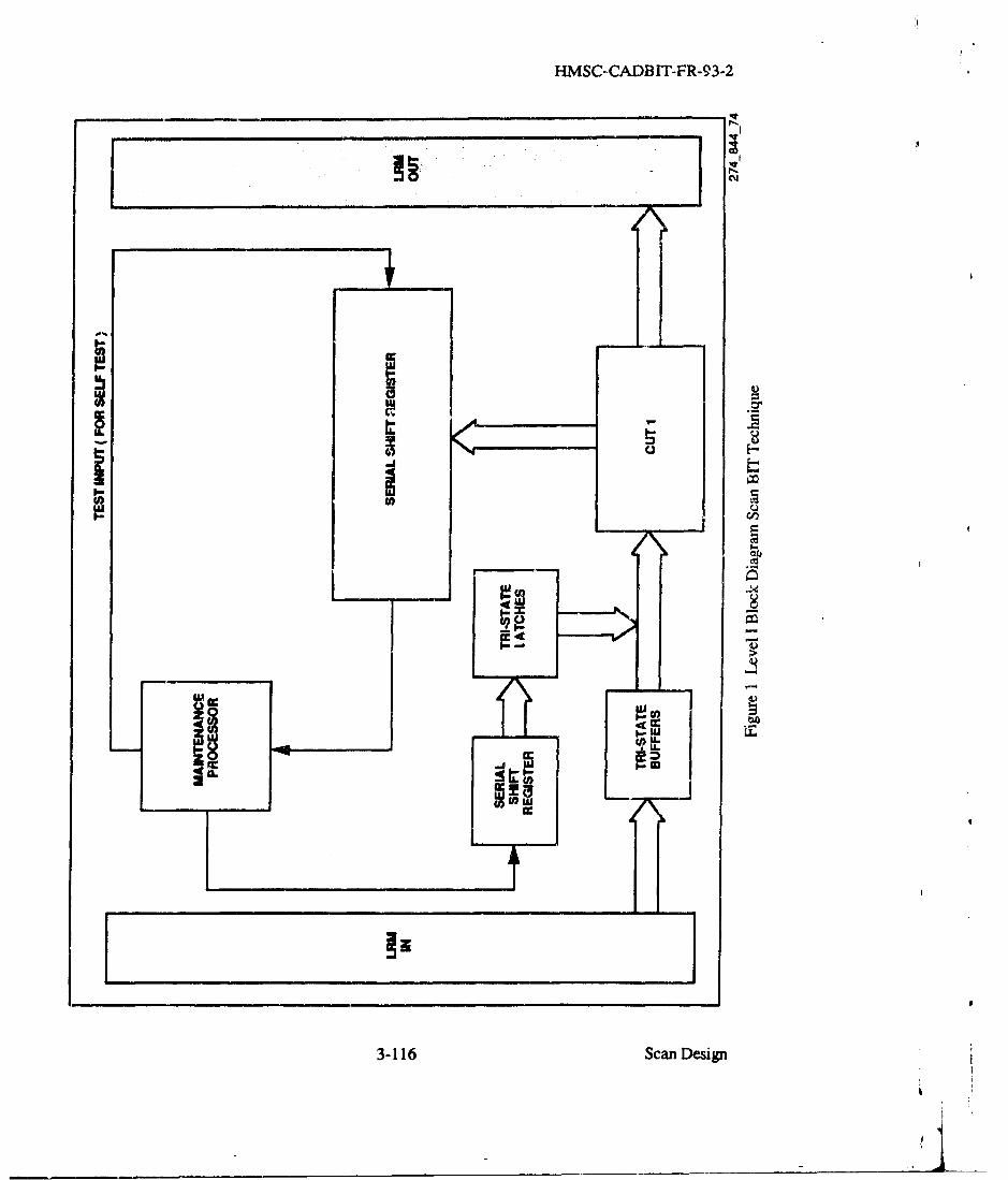
HMSC-CADB IT-FR-93-2
IIIc
0 H
3-11 cn e

HMSC-CADBrT-FR-93..2
zzii
IICL4
CA w
3-117 Sean Drzig

HMSC-CADB1T-FR-93-2
BIT TECHNIQUE: SCAN DESIGN
CATEGORY: FLOW CHART ! DESCRIPTION
Figure 3 shows the Flow Chart for this BIT te'chniquc.
1. Receive BIT INITIATE and set test inputs.
2. Enable first test loop (switches input MUX to test mcde).
3. Shift input test pattwrr into input register.
4. Load input data into input latch. Input additional sequential patterns if requireL
5. Parallel load output data into scan shift registers.
6. Apply READ scan clock and shift out SCAN data.
7. Reaid SCAN results and compare.
8. If test fails, set PassFail indicator to FAIL and end the test. If test passes, continue on tonext test.
9. Input additional sequential patterns if required.
10. Test. nxt loop if required by repeating Steps 2-9. If last loop has been tested, end the test bysetting the input MUX to normil mode.
3-118 Scan Design

.HMSC-CADBIT-FR-93-2
SET LOOP T]
ENABLE LOfj]
FLOAD TEST PAI"MRWINO NPffRE(CrnTrA
"IN, o ....- HNOY•E: MORE THAN ONEPATTERN MAY BE LOADEDINTO THE CUT jFOR INSTANCE,STEPPING A SEQUENTIAL
YES MOR~E MACHINE THROUGH A NUMBERPAITTERN OF STATES) BEFORE THE
OUTPUTS ARE SCANNED AMDChECKED AGOAMST THE OMR.
w 00
PARALLEL LOAD CUT Rr-WPONE--IN¶TO OUTPUT REGISTER
3M'-TI REGISTER RESPONSCE
INTO MMNTENANCEJ
< RESKSETO LOG AND REPORTR TEST 0 FAILURE
YES
YS MORE END
TO
(No
274_84475
Figurm 3 BIT Sequece Flow Chart For The Sc*m DIsign Technique
3-119 Scan Design

IMSC-CAD8 IT-.F'R.-93-2
BIT TECHNIQUE: SCAN DESIGN
CATEGORY: ADVANTAGES
1. Test input and SCAN" output latches are complWey exrnial to CUT.
2. Alhows for parallel load/serial scan output and seaial in/parallel load input modes of operation.
3. Only one shift clock is required.
4. Possible to take system snapshots.
CATEGORY: DISADVANTAGES
1. Serial in and serial out modes requim a large amnunt of test time.
2. Requires control of shift clock by m0intenance processor.
3. Requires a maintenance processor for control of the BIT test.
4. Requires a lot of board space and power for large systems.
5. Requires that the normal operation of the CUT be suspended during BUI testing.
3-120 Scan Design

HMSC-CADBIT-FR-93-2
BIT TF.CHNIOUE: SCAN DESIGN
CATEGORY: ATTRIBUTES
1. CONCURRENCY
* Non-concurrent, System operation must be suspended to perform the BIT test.
2. TECMNOLOGY
* Typically applicable to CUTs using digital technology.
* BIT circuit is implemented usiLg standard LS and ALS logic ICs, a crystal controlledmicroprocessor, and an EEPROM.
3. CUT MICROPROCESSOR REQUIRED?
* No.
4. CUT INTERNAL DESIGN REQUIRED?
* No. LRM inputs to CULT must be intercepted and multiplexed with BIT circuit test inputs.
5. AREA PENALTY
* Dependent on the number of CUTs and the number, of CUT inputs and outputs. Oneregister stage is needed for each CUT input and output.
6. WEIGHT PENALTY
* Roughly proportional to tr.c area penalty. Higher if CUTs have large numbers of outputsto be monitored or large numbers of inputs, or both.
7. POWER PENALTY
, Power penalty will depend on the number of SCAN registers (which depends on thenumber of CUTs and CUT inputs and outputs) and the microprocessor power dissipation.
3-12.1 Scan Design

HMSC-CADBIT-FR-93-2
BIT TECHNIQUE: SCAN DESIGN
CATEGORY: ATTRIBUTES, Contd
8. TIMING PENALTY
- Throughput Delay - In normal operation, there will be a slight increase in throughputdelay due to the addition of tri-state buffers to the input path,
- Test Time - During BIT testing, normal operation of the CUT is suspended. BIT test timeis long due to the serial transfer of data.
9. RELIABILITY
* Slight decrease in reliability due to the addition of a number of register chips and amaintenance processor. The number of register chips is proportional to the number ofCUTs and CUT inputs and outputs.
10. CONCEPTUAL COMPLEXITY
- Moderate complexity due to the presence of a maintenance processor.
11. HARDWARE/SOFrWARE&FIRMWARE
"* Hardware is used to implement the input and output registers, maintenance processor, testpattern memory, and control functions.
"• Software in the maintenance processor controls the loading of input test patterns, theloading of output data, and the comparison of output data.
12. DESIGN COST
• Hardware cost is minimal with the use of off-the-shelf chips. Additional non-recurringcost is incurred for the programming of the maintenance processor.
3-122 Scan Design

K HMSC-CADBIT-FR-93-2
BIT TECHNIQUE: SCAN DESIGN
CATEGORY: ATTRIBUTES, Contd
13. MEMORY REQUIREMENTS
• Test patterns and Good Machine Responses are stored in EEPROM.
* The maintenance processor has built-in EPROM and RAM to store program code and data.
14. BIT CIRCUITRY SELF-TESTABLE?
• The BIT circuit is fully self-testable. The maintenance pro~essor can be used to load andscan both the input test pattern and the SCAN output registers for proper operation. Also,test software can be written to check the function of the main program.
15. STAND-ALONE (SELF-CONTAINED BT?
"- Yes.
16. NOTES
• None.
3-123 Scan DesignL3

HMSC-CADBIT-FR-93-2
BIT TECHNIQUE: SCAN DESIGN
CATEGORY: DEFAULT DESIGN
Refer t Figure 4 for the Default Design schematic.
The SCAN BIT technique implemented in the Default Design provides hardware and software tosupport the testing of up to 4 CUTs. The circuitry for only 1 CUT is shown in the interest ofclarity (see the cross-hatched area of Figure 4). This design incorporates the default values for thenumber of CUT inputs (8) and CUT outputs (16) to be tested. These can easily be tailored to theparticular CUT by adding or deleting hardware.
Functionally, the SCAN technique is implementd using a maintenance processor to control thetest, EEPROM memory to store test patterns, an input shift register with parallel output to load thetest patterns into the CUT, a MUX to select between CUT normal inputs and test pattern inputs, anoutput shift register with parallel load to accept CUT test outputs and shift them into themaintenance processor, and associated glue logic.
The maintenance processor selected for the design was the Intel 187C51 8-bit Microcontroller. Itfeatures 4 configurable 8-bit ports, Port 0 through Port 3. Port 0 is multiplexed to put out the low-order address byte and to receive data during accesses to the EEPROM memory. Port 1 isconfigured as a general purpose test bus. It can be used to communicate the results of the BrT testto the system processor which can then be used to fault isolate errors to the component level. Port2 provides three address lines to the EEPROM as well as a number of signals to control the BITtest. It also outputs the _PASS/FAIL signal (Port 2, bit 7 or P2.7 for short) to the system. Port 3generates the read and write control lines to the EEPROM, accepts the BIT_INITIATE (P3.2)interrupt from the system, outputs the serial data to the input shift register, accepts input data fromthe output shift register, generates the clock to control the shift registers, and provides the controlsignals to generate the loop enables. The control signals are generated by software stored in theon-chip EPROM. Also, the software performs the comparison of the output data with the GoodMachine Response (GMR) and outputs the results through the _PASS/FAIL signal.
U2, a 54ALS373 Octal Latch, stores the low-order address byte as is typical for processors withmultiplexed address/data busses.
U3 is a 2817A 2K X8 EEPROM used to store test patterns for the BIT test and, optionally, GoodMachine Responses.
U4 is a 54ALS 138 3-line to 8-line decoder and enables one of 4 CUT BITs to be tested. It usesthree outputs from the maintenance processor, P3.3, P3.4 and P3.5, to enable BIT testing and toselect which channel is tested.
3-124 Scan Design

HMSC.CADBIT-FR-93-2
BIT TECHNIQUE: SCAN DESIGN
CATEGORY: DEFAULT DESIGN, Contd
The active ._LOOP_EN output for a particular channel selects the test pattern inputs, disables thenormal CUT inputs (U9 and U10), and enables the output shift registers (U 11 and U12).U5 is a 54ALS253 1 of 4 line data selector and is used to select which CUTs data output from theoutput shift register is routed to the maintenance processor data input (P3.0).
U6 (54ALS32) contains OR gates used to enable or disable the clock output (P3.1) depending theR/_W control output (P2.4) from the maintenance processor. U6A enables the RDCLK lineswhen the R/_W is high while U6B enables the WRCLK lines when R/_W is low.
U8 is a buffer/line driver for the DATA-OUT, RD.,CLK, WRCLK and LD lines coming out ofthe maintenance processor and the control logic.
U9 is a 54LS595 serial input shift register with parallel tri-state output latches. It is used to shift intest pattern data supplied by the maintenance processor (P3.0) through U8A. It uses the_LOOPEN signal from U4 to enable the latch outputs, the LD signal from the maintenanceprocessor (P2.3) through U8B to load the parallel output, and the WRCLK from U8B as a clockto shift in the data, Its outputs are bussed with the output of U10, a 54ALS244A tri-state bufferwhose inputs are connected to the LRM outputs which would normally connect to the CUT inputs.The LOOPEN signal is used to control which tri-state outputs are enabled. In this way the CUTinputs are selected to be either the test pattern inputs or the normal inputs from the LRM. Innormal operation, the U10 buffcrs are in-line with the inputs to the CUT adding a propagationdelay of 18 nsec maximum. The circuit can easily be expanded to accommodate more inputs bycascading 54LS595 shift registers and adding more 54ALS244A tri-state buffers. To cascade54LS595 chips connect the Q(, output (pin 9) to the serial input (pin 14) of the successive chip.
U 11 and U12 are 54ALS 165A 8-bit parallel in, serial out shift registers. The CUT output nodesbeing tested are parallel loaded into the register and then serially shifted out to the maintenanceprocessor (P3.0) through U5. The circuit can easily be expanded to accommodate more outputs byadding more chips. The QH output (pin 9) of each chip connects to the CLK input (pin 2) of thesuccessive chip. Control signals are the RDCLK (from U8A) used to shift the data out of theregister, LOOPEN (from U4) to enable the clock input to the shift register, and LD (from U8B) tocontrol whether the regisier is in the shift or load parallel data mode.
3-125 Scan Design
iI

HMSC-CADBIT-FR-93-2
BIT TECHNIQUE: SCAN DESIGN
CATEGORY: DEFAULT DESIGN, Contd
Two test signals are provided by the maintenance processor (P2.5 and P2.6) to test the input andoutput registers. TESTSCANREG inputs serial data from the processor into the output register.Data is shifted out in the usual fashion and checkedagainst the input for errors. For the other test signal, the input register is loaded with a test patternin the usual manner and data is shifted out to the maintenance processor through theTESTINPUTREG line for comparison. The software is also exercised completing the self-testof the BIT circuitry.
Test Bhgg : Any combinational circuit can be tested by loading the CUT inputs with a testpattern and checking the CUT output to a GMR. Sequential machines can also be tested by usingthe clock signal for the machine as one of the inputs to theCUT. The processor can be programmed to manipulate the clock and the CUT outputs can berested for any input condition in any machine state.
Certain limitations do apply to this technique due to its slow sped. For instance, outputs of one-shots cannot be tested if their pulse widths are short (< 100 msec).
Coclusga: The SCAN BIT technique can be useful to many applications using sequential orcombinational logic if normal operation of the CUT can be suspended during the BIT test, the slowspeed of the test can be tolerated, and the large hardware overhead is acceptable.
3-126 Scan Design

I.PASS/FAIL 40
R f AET AC>-.
*ATA~~T' I 130CATAI
~ft~ CTS ~ OATA INto.
I's*
V ice v **- - 3 ~ -
> -. I -3

HMSC-CADBrr-FR-93-2
- - ->P A R AL E E U
CaPARALEL-TST- U
_ ___ __ __ _
-. II. * "a
MODES to It TIST'O
al 11.1 9
%atf I$JI1O
CUT I OUPT
to To
IMP LEMENISIGN CAN TYPICAL~ IWPLEUENIATION FOR EACH CUr.
THI NS G CAN SUPPOuRT UP TO 4 CUTS.
Pigure 4 Scan Desifan - Default Design
3-127/1 28 (~ )Scan Design

ItMSC-CADB IT-FR-93-2
BIT TECHNIQUE: SCAN DESIGN
CATEGORY: BIT TECHNIQUE INSERTION DIAGRAM
Figure 5 shows the BIT Technique Insertion Diagram for this BIT technique.
BIT ELEMENT 1
1. Connect the BIT_INITIATE, _RESET, and _PASS/FAIL signals between the maintenanceprocessor of BIT ELEMENT I (BEl) and the LRM.
2. Connect the PARALLELTESTBUS outputs of BEI to the LRM.
BIT IFMENT ?
1. For CUT 1, connect WRCLK_0 output of BEl to BIT ELEMENT 2 (BE2). If there aiemore CUTs (up to 4 total), connect WRCLK_1-3 to the BE2s for those CUTs.
2. Connect the DATAOUTO from BE1 to BE2 of CUT 1. If there are more CUTs (up to 4total), connect DATA_OUTl-3 to the BE2s of the other CUTs.
3. Connect the normal CUT 1 inputs from the LRM to the BE2 associated with CUT 1. If thereare more CUTs (up to 4 total), connect the normal CUT inputs to their associated BE2s.
4. Connect the multiplexed outputs of BE2 to their associated CUT inputs.
5. Connect the TESTINPUTREG signal between BE1 and BE2.
,~11 BIT EN 1~.R
1. For CUT 1, connect the RD__CLK0 output from BE1 to BIT ELEMENT 3 (BE3). If thereare more CUTs (up to 4 total), connect RDCLK_1-3 to BE3 for those CUTs.
2. Connect the I.DJ0 AND _LOOP_EN_0 to both BE2 and BE3 associated with CUT 1. Ifthere are more CUTs (up to 4 total), connect LD-1-3 to the BE2s and BE3s of the remainingCUTs andLOOP_EN_1 to BE2 and BE3 of CU.T2, _LOOP_EN_2 to BE2 and BE3 ofCUT 3, and _LOOPEN_3 to BE2 and BE3 or CUT 4.
3. Connect the DATAIN_0 frorn BE3 TO BEI. If there are more CUTs (up to 4 total),connect DATAJIT . from BE3 to BE1 of CUT 2, DATA_IN_2 from BE3 to BE1 of CUT3, and DATA_IN_.3 from BE3 to BE I of CUT 4.
BT-ELEM[ENT 3
4. Connect all CUT test outputs to their corresponding BE3 parallel Cat inputs.
5. Connect the TESTSCANREG between BE3 and BEL.
3-129 Scan Design

HhISC-CADFIIT-FR-93-2
Cu.uj
0-I-i~U
00026~~.r4eI IrC
99
At6
j r .a1c
3-130 Scan Design

HMSC-CADBrT-FR-93-2
BiT TECHNIQMJE: SCAN DESIGN
CATEGORY: PENALTY EQUATIONS
AREA (sq.ln.) = Su•v (ni * aj) + 15% figr aace's
WEIGHT (gins) = Sum ( ni * wj ) + 10% for solder
POWER (aW) - Sum (ni * pi)
TEST TIME (ns) =
DELAY (nsý =
E.planation of Symbols Used.
Sam = Sum over Parts in BIT Techniqale Parts Table (i=1 to ll)ni = Number of component packages for i-th part in Parts Table
ni is calculated according to Componeut Deternination Equationsai Arew in sq.in. of i-th pr in Parts Tablepi = Power dissipation ir mW (typical) for i-th part in Parts Tablewi = Weight in grams of i-th part in Parts TableVi = User-supplied value for i-th variable (see Variable Definitions)
CATEGORY: BIBLIOGRAPHY
1. E. J. McCluskey, "A Survey of Design for Testability Scan Tecimiques",VLSI Design, December 1984
2. B. Eichelberger and T. W. Williams. "A Logic Design StrtictuTe for LSI Testability",Fourteenth Annual Design Automation Conferencc, New Orleans, June 1977, pp. 462-467
3. M. J. Y. Williams and J. B. Angell, "Enhancing Testability of Large Scale IntegratedCircuits Via Test Points and Additional Logic", IEEE vol no. I (Jan 1978) pp.4 6 -6 0
3-132 Scan Design

HMSC-CADBIT-FR-93-2
DIGITAL WRAPAROUND
BIT TECHNIQUE DATA PACKAGE
CATEGORY: SHORT DESCRIPTION
Digital Wraparound is a non concurrent Built-In-Test (BI') technique. This technique consists ofhardware and software (firnware in Read-Only Memory (ROM)) and specifically requires amicroprocessor, some digital output devices and some digital input devices on board as parr of theCircuit Under Test (CUT).
The technique consists of adding the necessary circuitry so that upon BIT INITIATE, the digitaldata leaving the digital output devices can be mruted to the digital input device on the LineRepiaceable Module (LRM) by adding digital gates to %Tap the outputs around to the inputs. Arappropriate BIT routine is stored in ROM along with test data to control the data transfer andcompare the data received with the data transmitted. A mismatch will indicate a failure.
The Microprocessor BIT technique (a related digital BIT technique), checks out the internalcomponents of the microprocessor system. The wraparound BIT can be used to exteiid themicroproccsr BIT to include the I/O.
Figures 1 and 2 show the Level I and 11 Block Diagrams for this BIT technique.
3-133 Digital Wraparound

fiMS(>CADBrI -FR-93-2
0-0
3-134 DigitalWxipwanid

FIMSC-.>&J)BT-FR-93- 2
40.
3-13 -l igti Wrm

HMSC-CADBIT-FR-93-2
BIT TECHNIQUE: DIGITAL WRAPAROUND
CATEGORY: FLOW CHART I DESCRIPTION
Figure 3 shows the Flow Chart for this BIT technique.
1. A 'BIT INITIAT' signal is input to the LRM, so testing can begin.
2. Initialize the Circuit Under Test and set the Pass/Fail Flip-Flop to PASS.
3. Bt fore applying a signal, enable the wraparound gates that are going to be used for thatparticular test and disable system input and output buffers.
4. Apldy the ROM test pattern to the output device(s).
5. At this point, the test data is routed from the outputs through the proper enabled wraparoundgazes and into the inpu. device(s).
6. Dc.lay and strobe the memory chip to send the expected results to the microprocessor.
7. Micoprocessor reads the results from the input devices(s) and compares it with expectedresult from memoy.
8. If comparison fails, set Pass/Fail Flip-Flop to FAIL and end test. If comparison passes,cotp dnue to next step.
9. If this is the last test pattern, then end the test. Otherwise, go back to STE? 4 and continue.
3-136 Digital Wraparound

HMSC-CADBIT-FR-93-2
PASS-F=AIL FF TO PA8SS
ANDO UPUT IENABLE WRAPAROUND
I APPLY ROM TEST PATTERN ITO OUTPUT DEVICE(S)
ROUTE DATA FROM OUTPUTS Ijo THRU WRAPAROUND GATES
TO INPUT DEVICE(S)
DELAY & STROBE MEMORYRESULTS TO
MICROPROCESSOR
APPLY NEXT ROM TEST MICROPROCESSOR READS
PAITrERN INPUT DEVICE ANDOUTPUT DEVICE(S) COMPARES WITH EXPECTED
RESULT FROM MEMORY
NO SET PASS/FAJI.PASS ?FF TO FAIL
YE8
NOE
274..844-79
Fig= 3 BIT Sequee Flow Chart For Digital WraparoLnd
3-137 Digital Wraparmund
'I
HMSC-CADBrT-FR-93-2
BIT TECHNIQUE: DIGITAL WRAPAROUND
CATEGORY: ADVANTAGES
1. Only, requires minimal hardware and is a conceptually simple design which is easy toIMpIemCnL
2. Chips that are needed are readily available (the wraparound device is generally standard gatesof the same logic family used in the digital I/O.)
3. This technique may also be used in conjunction with "MICROPROCESSOR BIT"', anotherComputer-Aided Design for Built-In-Test (CADBIT) technique, t extenid the BIT coverageto include the I/0 chips (which are not normally checked out with the Microprocessor BITtechnique.)
3-138 Digital Wraparound

HMSC-CADBH'-FR-93-2
BIT TECHNIQUE: DIGITAL WRAPAROUND
CATEGORY: DISADVANTAGES
1. This technique only checks out a small portion of the LRM.
2. If the number of test pattmis needed to completely test the digital 1/O is large (for example, aMIL-STD- 1553B interface), then additional ROMs may have to be added to store the testpatterns. This will incricase the real estate penalty. However, if the I/O devices arm simplybuffers, only a few patterns will be required, and most ROMs will have spare locations.
3-139 Digital Wraparound

IHMSC-CADBIT-FR-93-2
BIT TECHNIQUE: DIGITAL WRAPAROUND
CATEGORY: ATTRIBUTES
1. CONCURRENCY
* Non-concurrent
2. TECHNOLOGY
. Digital
3. CUT MICROPROCESSOR REQUIRED?
*Yes
4. CUT INTERNAL DESIGN REQUIRED?
* No
5. REAL ESTATE PENALTY
• Small - Only requires several integrated circuit packages of gates.
- ROMs - Depends on number of test patterns (as patterns increase, any spare ROMlocations way be depleted, therefore an additional ROM(s) may have to be added).
* If number of I/O lines is large, there will be a corresponding increase in number ofwraparound gates required
6. WEIGHT PENALTY
* Small - Proportional to real estate penalty
7. POWER PENALTY
* Small - Just requires additional power to wraparound gates and additional ROM if needed.
8. RELIABILITY IMPACT
* Minimal impact since only a few gates of the same logic family as the //O devices arcadded.
3-140 Digital Wraparound

HMSC-CADBIT-FR-93-2
BIT TECHNIQUE: DIGITAL WRAPAROUND
CATEGORY: ATTRIBUTES, Contd
9. TIMING PENALTY
- Throughput delay - equal to propagation delay of I/O buffer.
STest time - sum of test initiation time and number of test patterns multipiied by the patternapplication rate.
10. CONCEPTUAL COMPLEXITY
• Straightforward
11. HARDWARE/SOFT WAREI MBO
• Hardware present/est patterns in firmware.
12. STANDALONE?
*Yes
13. IS BITE SE.F-TESTABLE?
- No.
14. DESIGN COST
* Minimized since wraparound chips needed are readily available.
* The CUT microprcessor can also be used for other BIT techniques.
* Engineering time to create patterns depends on complexity of I/O chips to be tested.
15. MEMORY REQUIREMENTS
• ROM needed to store test patterns
16. NOTES
* None
3-141 Digital Wraparound

HMSC-CADBIT-FR-93-2
BIT TECHNIQUE." DIGITAL WRAPAROUND
CATE.GORY: DEFAULT DESIGN
This section desciibes the scquence of events for the DIGITAL WRAPAROUND BIT technique
default design. Refer to Figure 4 for the Defiult Design schematic.
1. When the microconn¶roer receives a TESTIN1ITATE signal to its port P1.4, the. test begins.
2. Output from P1.6 enables wraparound gates U8A and UMB. The inverted P1.6 signaldisables inputs and outputs octal buffers U7A, U7B, U9A, and U9B.
3. Set the ParFail indicatok P1.5 to PASS.
4. Apply test pattern to U4 as the output device. Routes the pattern back to the input devicethrough U8A and U8B as the wraparound gates. The microconurollez captures the responsethrough the input device U5 and compares it with expected results from memory intemally.
5. Step 4 is repeated until all test patterns pass. If any comparison fails, set Pass/Fail indicatorP1.5 to FAIL and end test.
6. When test is finished, output from P1.6 disables wraparound gates U8A and U8B. Theinverted P1.6 signal enables inputs and outputs octal buffers U7A, U7B, U9A, and U9B."The circuit resumes normal operation.
3-142 Digital Wraparound

HMSC-CADBr!T
U6
iCUT____________S TS-1 NrI-IIS s8
OUSOMO.) S M
4ALS373 t Tl
_Oc BUS (7: U1A2 2
U3 RI TV
RIQT
".% F to 4 at ! TI
".7 F': aA4 TV
USI~R TI10
OUS2BUS (77. I; T
to le- RI TI
I'L~~~U' pP1172:233 A2T
is-EYAS S3
Fiur 4A Diptu Wj3POfl - Atf~I TO~
it 3MST14 (5)N
>DUg tso s
so so

)B7.-FR-9 HMSC-CADBrr-FR-93-2
UG
USS (7101
c
---
+5V
UP54RL3373 - 411 10,11 -02 T2-OC eUS 1 (7: 0) - as TZU3 All Yt I
10 IQ 7258-1220 PC S4 4ý630 30
.- %a No- 50 so
so so it. T.1At ''270 70 02 -nali2Y, 2AS YSso so a 44 TjON 'T %3
U4-- BUSI (Isle) 87 SMALS373 U80
-oc BUS317i 54ALS2 Mec c -0
Is Al 7142 TZ
10 so A3 T3
It 40 No All TOso so
11'0 7'0* 54 11
At 10 so i
-- c J
to - ý' I T'2'
us L i
U90
10 A D
-E> 5 y S-( to to - T SYS-04Tjo so 81 Ato to - 02 T2
so so 03 T3
IQ 60 - At T4
?a 70 -
BUS2 M 9) so 00
elýu
'FISS/FR;'
Figum 4 019itill Wmparoumi - Default DOSiP
lwmpw 3-143/144 Digital WmpuvuW

HMSC-CADBI r-Fk-93-.2
BIT TECHNIQUE: DIGITAL WRAPAROUND
CATEGORY: RkT TECHNIQUE INSERTION DIAGRAM
Figure 5 shows the BfT Tecliniqie Block Di6grsrn for this BIT techaiique.
Connections instrucions wt shwrn hi Figres 6-9 gks follows:
Figure 6- Connection instructicas for BTID Block 1 - Output Buffers
Figure 7 - Corm.ectiun instractions for BTh) Block 2 - Digital Gates
Figure 8 - (onnzcfion instruction- for BTID Block 3 - Input Buffers
Figure 9 - Connection instiuctions for PRiss!Fail Flip-Flop
3-145 Digital Wraparotud

..HMSC-CADBIT-F'R-93-2
I-I
0
S..... ...
ni 5ag;
3-146 Digital Wraparound

- -- ________________
HMSC-CADBJT-FR-93-2
I0illi
"''Ii
Ii.' 4Ililfi Iii'''q!'� I! I!111111 1
. . .
3-147 Digital Wrdpawund

HMSC-CAO)Br~rT4R 9..9.2
II
F-I -Y 1 I -,
334'igm rqon

HMSC-CADE~rf-FR.93-2
,v- VI
ye1 I- II
3-149 Digital Wraparound

HMSC-CADBIT-FR-93.-2
S- .0
GoJ
3I5'igtl'rpon

HMSC-CADBIT-FR-93-2
BIT TECHNIQUE: DIGITAL WRAPAROUND
CATEGORY: VARIABLE DEFINITIONS
Variable Variable Definition Units
vi. Number of CUT outputs to test none
v2. #Test patterns for Digital Wraparound BIT patterns
v3. Test pattern application rate for Digital Wrap BIT patterns/sec
V4. CUT initialization time sec
CATEGORY: COMPONENT DETERMINATION EQUATIONS
The number of units (as represented by CAD symbols) and component parts (physical packages)
reqtuied to implement the Default Design are calculated as follows:
BIT Technique Parts Table (for Default Design)
"In"dex, i Piat Number Part Type Units Required, uiI 54ALS04B INVERTER - 1"
2 54ALS244A BUFFER 3 * ceil (vl / b)
The number of Component Parts Required is calculated (for i-th part) as follows:
ni = ceil ( ui / uppi)
Explanation of symbols used:
ni = Number of components (physical packages) required for i-th partui = Number of units (CAD symbols) required for i-th partuppi Number of units/package for i-th part (from Table 4.0)ceil = Round up to nearest integer (e.g. 5.3 is rounded to 6)b = Number of data bits for part (from Table 4.0)vi = User-supplied value for i-th variable (see Variable Definitions)
3-151 Digital Wraparound
Ii

HMSC-CADBlT-FR-93-2
BIT TECHNIQUE: DIGITAL WRAPAROUND
CATEGORY: PENALTY EQUATIONS
AREA (sq.in.) = Sum ( ni * ai ) + 15% for taces
WEIGHT (guns) = Sum ( ni * wi ) + 10% for solder
POWER (mW) = Sum (ni * Pi)
TEST TIME (ns) = (v4 + tBUFFER) + ( V2 * (l/v3)) + (v4 + tBUFFER)
DELAY (ns) = 2 * tBUFFER
Explanation of Symbols Used.
Sum = Sum over parts in BIT Technique Parts Table (i=l to 2)ni = Number of component packages for i-th part in Parts Table
ni is calculated according to Component Determination Equationsai = Area in sq.in. of i-th part in Parts TablePi f Power dissipation in *mW (typical) for i-th part in Parts Tablewi = Weight in grams of i-th part in Parts Tablevi- User-supplied value for i-th variable (see Variable Definitions)tBUFFER = Max delay for BUFFER from Table 4.0
CATEGORY: BIBLIOGRAPHY
None requiwj.
3-152 Digital Wraparound
HMSC-CADB1T-FR-93-2
PSEUDORANDOM PATTERN GENERATOR WITHMULTIPLE INPUT SIGNATURE REGISTER
(PRPG/MISR)
BIT TECHNIQUE DATA PACKAGE
CATEGORY: SHORT DESCRIPTION / DIAGRAM
This non-concurrent self test method can be implemented in hardwa-e without requiring numeroustest patterns or good machine responses to be stored internally Testing begins upon activation of atest initiate signal, after which the test control logic :aidalizes the Pseudorandom Pattern Generator(PRPG), which then generates and applies a set of pseudorandom test patterns to the Circuit UnderTest (CUT) by multiplexing out the primary inputs and multiplexing in the PRPG outputs. APRPG with n outputs will pseudorandomly cycle through all but one of the possible n - bit binarypatterns, which is a total of 2n -I possible bit patte'ns. In order to determine if the CUT'sresponse to these patterns is correct, the outputs of the CUT are connected in parallel to theMultiple Input Signature Register (MISR) with m inputs, which compresses the test result data intoa single m - bit signature. If the test result signature is identical to the good machine signature, thetest passes. This test method is advantageous because one achieves a substantial amount of testingwith a relatively snmall amount of hardware.
Figures I and 2 show the Level I and II Block Diagrams for this BIT technique.
3-153 PRPG/MISR

. ........... ...
HMSC-CADBrr-FR-93-2
V.-
IL
U.12
.2~ _ _
_________
k3-154 PRPG/MISR

HMSC-CADBIT-FR-93-2
cm~J
I--
4100
bA
3-155 PRPG/MISR

HMSC-CADBIT-FR-93-2
BIT TECHNIQUE: PRPG/MISR
CATEGORY: FLOW CHART / DESCRIPTION
Figure 3 shows the Flow Chart for this BIT tecnique.
1. Receive BIT inijate and start test.
2. Initialize CUT, reset circuits, seed PRPG, select CUT inputs to be output of PRPG.
3. Clock Pseudorandom Pattern Generator and apply test pattern to CUT.
4. Test pattern ripples through CUT.
5. Clock multiple input signature register with falling edge 'of clock.
6. Apply next test pattern; continue until all patterns are applied.
7. Compare GM signature with CUT signature; set PASS/FAIL.
8. Select CUT inputs to Ix- input from system.
3-156 PRPG/MISR

HMSC-CADBIT-FR-93-2
RECEIVE BIT INITlAl
INITIALIZE CUTCOUNTERS, RESET
PASS/PAIL FF TO PASISEED PRPG
S CLOCK PRP (RISING EDGE 1AND APPLY TEST PATTERN
274_844_87
Figure 3 BIT Sequence Flow Chart For PRPG/MISR
3-157 PRPG/MISR

HMSC-CADBIT-FR-93-2
1;T TECHNIQUE: PRPG/MISR
CATEGORY: ADVANTAGES
1. PRPG/MISR is a very cost effective BIT technique because large numbers of test patterns
can be generated without the need for large hardware overhead.
2. There is no software overhead.
3. Multiple input signature registers allow multiple CUT outputs to be tested without storinghuge good machine responses in ROM.
CATESORY: DISADVANTAGES
1. A PRPG cannot systematically generate specific pairs of test patterns in sequence to delectfaults in certain sequential logic designs.
2. More pseudorandom patterns may be required to achieve a desired percentage of faultcoverage than a set of test vctoi-s that can be individually specified, such as in the On-BoardROM technique.
3-158 PRPG/MISR

hMSC-(.:ADfiT.FR,-93-2
BIT TECHNIQUE: PRPG/MISR
CATEGORY: ATTRIBUTES, Contd
9. CONCAEPTrUAY, COIPL.XWITY
SSu-Ightforward
10. HARDWAR!EV/SoFWARE/f IRMWARE
* Hardware
It. IS BITE SELF-TESTABLE?
* No
12. DESIGN COST
- Minimal with off the shelf chips available.
13. STAND-ALCNE (SELF-CONTAINED) BIT?
*Yes
14. WEIGHT PENALTY
SRoughly proportional to area penalty.
3-160 PRPG/MISR
I,

HMSC-CADBIT-FR-93-2
BIT TECHNIQUE: PRPG/MISR
CATEGORY: DEFAULT DESIGN
This se, ction describes the sequence of events for the PRPG/MISR BIT ttchnique default designl.Refer to Figure 4 for the default design schematic.
I1. At the beginning of the test, the TESTINITIATE signal goes low and triggers the following:
a. Presets U1A test control flip-flop and enables TESTCLOCK signal to activatecounters, PRPG, and MISR.
b. While the TESTN1TIATE signal holds low, the next rising edge of theTESTCLOCK signal loads zeroes into the synchronous 4-bit binary counters U18 andU19.
c. Disables normal inputs of CUT. Configures U 16 and U 17 MUX to select inputs fromPRPG to CUT.
d. Enables U20 8-bit identity comparator, disables U21A and U21B octal buffers andplaces the outputs of C(UT into high impedance.
e. For PRPG, presets UIB flip-flop and clears U3A, U3B, U4A, U4B, U5A, U5B, andU6A flip-flops.
f. Resets all resetable logics in the CUT.
g. For MISR, presets U6B flip-flop and clears U7A, U7B, U8A, U8B, U9A, U9B, and
U10A flip-flops.
h. Clears the Pass/Fail flip-flop U10B to PASS.
2. After the TEST_INRTIATE signal goes back to high, the TESTCLOCK signal startsincrementing counters U18 and U19. While the PRPG, CUT, and counters are drivendirectly by TEST_CLOCK, the MISR is driven by falling edge of the TESTI>CLOCK toensure enough delay time for the PRPG !cst pattern to ripple through the CUT before itreaches the MISR.
3-161 PRPG/MISR .1

RLMSC-CADBIT-FR-93-2
BIT TECHNIOUE: PRPG/MISR
CATEGORY: DEFAULT DESWGN, Contd
3. After 255 TEST.-CLOCM cycles (2A8- 1 2-55), U19/RCO outputs a high and indicates theend of the test:
a. Clears UIA test control flip..flop and disconnects TEST-CLOCK signal to counters,PRPG, and MISR.
b. Enables normal inputs of CUT. Configures U16 and (317 MUX to select inputs fromnormal inpus to cur.
c. Disables U20 8-bit identity comparator and enables TJ21A and U21B octal buffers fornormal CUT outputs.
d. Clocks in the result of the comparison of Good Machine Response and compressedsignature. This result is registered by the Pass/Fail flip-flop LIOB.
4. The circuit resumes normal operation and it will go into test mode when theTEST_INITIATE signal goes low again.
3-162 PRPGtMISR

Not, 4- mup.slatl,0-3. b"ol Ha60#4 tA1'
'4T41"AT It - -- -. -
-' -. -
' . Ia
CUT..INPUIE7i,
Lu',,
VIS -- c -tal*1lS. -tt I ~$ .A
-ftID igre4PRCJIS
3-J63/I6.

HMSC-CADB1T-FR-93-2
4..4
C U TS
Itoo...
t ti
IS.1
Figure 4 pRpGI/MISR - Default Design
3-163/164 ()PROG/MISR

HMSC-CADBIT-FR-93-2
BIT TECHNIQUE: PRPG'MISR
CATEGORY: BIT TECHNIQUE INSERTION DIAGRAM
Figure 5 shows the BIT Technique Insertion Diagram for this BIT technique.
BIT ELEMENT 1:
1. Connect the control gates and Flip Flop to the control counters.
2. Connect the LRM inputs to the MUX inputs.
3. Connect the MUX outputs to the CUT inputs
BIT ELEMENT 2:
I. Connect the seed counter output to the inputs of PRPG.
2. Cornect the output of PRPG to the CUT inputs.
BIT ELE14ENT 3:
1. Connect the CUT outputs to the input of MISR.
BIT ELEMENT 4:
1. Connect the the output of MISR to the comparator.
2. Connect the output of the comparator to the input of the D input of the Pass/Fail Flip Flop.
3. Connect the Reset signal to the Pass/Fail Flip Flop CIR signal line.
3-165 PRPG/MISR
,_ _ .1

HMSC-CADBrT.FR-93-2
I.-
0 cc ~ 0
_ _ _ I-
0
3-166 PRPG/MISR
HMSC-CADBIT-FR-93-2
BIT TECHNIQUE: PRPG / MISR
CATEGORY: VARIABLE DEFINITIONS
Variable Variable Definition Units
v1. Number of CUT inputs none
v2. Number of CUT outputs to test none
v3. Maximrnum propagation delay through CUT ns
V4. CUT initihlization time S4c
v5. Internal Design OK? (Suitability Attribute) 0 if YES, 1 if NO
CATEGORY: COMPONENT DETERMINATION EQUATIONS
The number of units (as represented by CAD symbols) and component parts (physical packages)
required to implement the Default Design are calculated as follows:
BIT Technique Parts Table (for Default Design)
Index, i Part Number Part Type Units Required, ui
1 54ALS04B INERTER 22 54ALS08 AND GATES 33 54ALS74A FLIP-FLOP I + vl + (v5 * v2) +14 54ALS86 EXCLUSIVE-OR 3 + (v2 + 3)5 54ALS157 SELECTOR/MUX ceil (vj / b)6 54ALS161B COUNTER ceil (v 1 / b)7 54ALS244A BUFFER ceil (v2 / b )8 54ALS521 COMPARATOR ceil (v2 / b)
The nimnber of Component Parts Required is calculated (for i-th part) as follows:
ni f ceil ( ui / uppj )
Explanation of symbols used:
ni Number of components (physical packages) required for i-th partui = Number of units (CAD symbols) required for i-th partuppi = Number of units/package for i-th part (from Table 4.0)ceil Round up to nearest integer (e.g. 5.3 is rounded to 6)b Number of data bits for part (forn Table 4.0)vi f User-supplied value for i-th variable (see Variable Definitions)
3-167 PRPG/MISR

HMSC-CADBrT-FR-93-2
BIT TECHNIQUE: PRPG / MISR
CATEGORY: PENALTY EQUATiONS
AREA (sq.in.) - Sum ( ni * ai ) + 15% for traces
WEIGHT (gins) = Sum ( ni * wi ) + 10% for solder
POWER (mW) = Sum (ni * pi)
TEST TIME (ns) = Max (v4 * 109 ,50) + ( p * 2M * (tMISR + v3)) + tCOMP + rFF
DELAY (ns) tMUX + tXOR + v5*tFF + tBUFFER
Explanation of Symbols Used.
Sum = Sum over parts in BIT Technique Parts Table (i=l to 8)ni f Number of component packages for i-th part in Parts Table
ni is calculated accoriing to Component Determination Equationsai = Area in sq.in. of i-th part in Parts Tablepi= Power dissipation in mW (typical) for i-th part in Parts Tablewi = Weight in gams of i-th part in Parts Tablevi = User-supplied value for i-th variable (see Variable Definitions)M = Design margin = 1.2p = Number of test paterns = 2v I 1tMISR = MISR time = tFF + tXORtMUX = Max delay for SELECTOR/MUX from Table 4.0tCOMP = Max delay for COMPARATOR from Table 4.0tEF = Max d&lay for FU,-P-FLOP from Table 4.0tXOR = Max delay for EXCLUSIVE-OR from Table 4.0tBUFFER = Max delay for BUFFER from Table 4.0
3-168 PRPO/MISR

HMSC-CADB IT-FR-93-2
BIT TECHNIQUE: PRPG/MISR
CATEGORY: BIBLIOGRAPHY
BILBO - Built-In Logic Block Observation Techniques79 - Koenemann, Mucha, Zwieoff - 1979 IEEE Test Conference
81 - Segers - 1981 IEEE Test Conference -A Self-Test Method for Digital Circuits
STUMPS - Self Testing of Multi Logic Modules82 - Bardell, McAnney - 1982 IEEE Test Conference
83 - Komonytsky - Electronics 1983 -Synthesis of Techniques Creates Complete System Self-Test
84 - Butt, El-ziq - 1984 International Test Conference - Impact of Mixed-Mode Self-Test On LifeCycle Cost of VLSI Based Designs
84 - LeBlac - 1984 IEEE Design & Test of ComputersLOCST: A Built-In Self-Test Technique
85 - Bhavsar - 1985 International Test Conference -"Concatenable Polydividers': BIT-Sliced LFSR Chips For Board Self-Test
86 - Sabe, Johannsen, Yau - 1986 Custom Integrated Circuits Conterence - Genesil SiliconCompilation and Design for Testability
3-169/3-170 PRPG/MISR

=.1
HMSC-CADBIT-FR-93-2
COMPARATOR
BIT TECHNIQUE DATA PACKAGE
CATEGORY: SHORT DESCRIPTION
Comparators can m*edily be incorporated into hardware designs to achieve Built-In-Test (BI)capability for a large variety.of functions with minimum expense. With this approach, CircuitUnder Test (CUT) stimuli, which are generated by the Line Replaceable module (LRM), areapplied to P CUT and the outputs of the CUT are applied to a comparator along with a referencesignal. The outputs of the CUT are compared to the reference signal and the comparator outputs aPASS/FAIL signal. For some applications, it will be necessary to process the (UT outputs withthe addition of signal processing circuitry before feeding the ze;ult to the comparator.
The Coznparator BIT technique allows for either including a signal source as part of the BIThardware or for receiving the test signal from outside the LRM. If multiple channels are present onthe CUT, analog switches can be added to distribute test signals to various channel inputs andanalog multiplexers to distribute the CUT outputs to the comparator for analysis.
Due to the wide variety of processing circmits available (e.g., frequency to voltage converters,RMS to dc, peak detectors, etc.), together with benefits gained from signal multiplexing, theComparator BIT technique lends itself to a wide variety of applications.
Due to the wide variety of processing circuits available, (e.g. frequency to voltage converters,sample and hold circuits), together with benefits gained from signal multiplexing, theCOMPARATOR BIT TECHNIQUE lends itself to a wide variety of applications.
Figures 1 and 2 .'xw the Level I and [n Block Diagrams for this BIT technique.
3-171 Comparator

HMSC-CADBIT-FR,-93-2
W0
~C,
3I7 onaw

HMSC-CADBIT-FR-93-2
4K iRn I-cc . )
19,000
±O3318 1INNYHOJ.fldLflo
3-173 Cornparator

HMSC-CADI~lT-FR-93-2
BIT TECHNIQUE: COMPARATOR
CATEGORY: FLOW CHART I DESCRIPTION
Figure 3 shows the Flow Chart for this BIT technique.
I. Initiate test by sending a negative going pulse to the TEST INfTIATE line.
2. Set the counter to zero. Set the Pass/Fail FF to PASS.
3. Apply the test signals to the CUT.
4. Select the CUT output to be processed or fed directly to the comparator.
5. If required, process the output by converting the parameter of interest (AC, RMdS, frequency,peak value, etc.) to a DC value. Route the signal to the comparator.
6. If the signal falls outside the limits of the comparator, set the PASS/FAIL FF to FAIL.
7. Determine if output is the last one to be tested. If it is, end the test.
8. If the last CUT output has not been tested, increment the counter and repeat Steps 4 through7.
3-174 Comparator

HMSC-CADBIT..FR-93-2
( ~INMTATE 'TEST )
SET COUNTER TO 0SET PAWSdFFAIP.
_.FF TO PASS , ,
E SIGNA LTC CUT
(DIRECT OR PROCE.SSED) TO BI
FED TO THE COMPARATOR
PROCESS THE SIGNAL BY-ONVEMWING TrE PARAMETER OF
INTEREST (AC, DC, RVA3, FREOUENCPEAK, ETC.) TO A DC VOLTAGE AN
ROUTE TO COMPARATOR
r.uNEIjCOMPRTR - y PASS/FAIGETETS-A FF TO FAIL
SIGNAL TIESTED-
274844_91
Figure 3 BIT Sequence Flow Chart For Utilizing Comparator Testing Techniques For N ChannelsOr Signals
3-175 Comparator

HMSC .CADBlFT-FR-93-.2
BIT TECHNIQUE: COMPARATOR
CATEGORY: ADVANTAGES
" The Compa; ator BIT can be used to verify the amp!dcude and frequency of many klnds ofsignals (DC, AC, RF, AM, and FM m.lulaied signals, digital pulses, and others) ifapprolriate signil processing is provided.
a Ar. unlimited rumber of test point signals can be monitored by one circu't with the use ofmultiplexers.
" Circuit components are common and can. be purchaseýd off the shelf from a wide variety ofvendors.
" The high input impedance of the window comparator and scaling circuits place very iittieload ou circuit outputs.
CATEGORY: DISAOVANTAGES
" The reference signal must be accurately maintained. Any dcviation from the desiredreference could cause erroneous BIT results.
" Frequendy, additional power supplies are required as either op amp power supplies or acreference voltage supplies.
" The analog switches vsed to switch the CUT input lines between the test signals and theactual LRM signals add 751 of on resistance to the CUT inputs which could slow downthese inputs."CUT outputs that are to be BIT tested must be scaled to fit vAithin the window of thecomparater, i.e. they must have the sane tolerance band as that of the comparator.
" Brf circuitry requires a clock sigial ta control channel selection and to allow properetdeling of analog signals before measurement is made.
" For statid (dc) test signals, resistor values must be selected. For more complicated testsignals, circuitry must be added to generate, those signals.
3-176 Comparator

HMSC.CADB IT- PR-9'.2
931T 7ECHNIQU-,. COMPARATOR
CATEGORY: ATTRIBUTES
1. COiU}."UEIN•Cv
* NOi coruncurlrit
2. 1ECHNGLOGY
"* Typically applicable to circuits using current ANALOG techi.ology.
"• E.isztig off-the shelf anaiog and digital integrated circuits are used for the BIT circuit.
3. CUT MICROPROCESSOR REQUIRED?
- No
4. CUT INTERNAL DESIGN REQUIRED?
* BIT cimaitry is external to the C1T.
5. AREA PENALTY
" The use of signal multiplexing with the comparator teclnique reduces the real estatepenalty incurred in contrast to the use of concurrent tech•iques such at redundancy. Thisis particularly true if large numbers of circuits ,=e to be. BIT tested.
"* If signal Processing circuits are required, the real estate penalty increases proportionately.
"• Required real estate for implementatioru of the technique increases as the number of CUTsignals tested increases. The amount of real estate required can be minimized with the useof multiplexers.
"• The necd for resistors and capacitors adds to the real estate penalty.
"* The addition of gating circuitry may be necessary for enabling and latching.
3-i77 Comparator

H-*MSC-CADBUIT-FR-93-2
BIT TECHNIQUE: COMPARATOR
CATEGORYr ATTRIBUTES, Contd
6. WEIGHT PENALTY
" The use of signal multiplexing reduces the weight penalty compared with concurrenttechniques. This is particularly true if large numbers of circuits are to be BIT tested.
" If signal processing circuits are required, the weight penalty increases.
7. POWER PENALTY
* Signal multiplexing reduces the power penalty over concurrent techniques.
* If signal processing circuits are required, the power penalty increases proportionately.
8. TIMING PENALTY
"* Throughput delay"• During normal operation, the Analog Switches placed in series with the CUT input lines
add an on-resistance of up to 750, which could affect CUT input circuit speed.
"• Test Time
" During BIT, normal operation of the CUT is suspended while the CUT is being tested.
9. RELIABILI Y IMPACT
" The failure rate goes up proportionately with the number of components added for the BITand signal processing circuitry.
" The input switches are the only in-line components that could cause a critical systemfailure.
3-178 Comparator

HMSC-CADB1T-FR-93-2
BIT TECHNIQUE: COMPARATOR
CATEGORY: ATTRIBUTES, Contd
10. CONCEPTUAL COMPLEXITY
• Straightforward.
11. HARDWARE/SOFTWARE/FIRMWARE
• BIT circuitry uses analog switches and multiplexers, comparators, and digital logic toimplement the BIT technique. If signal processing circuits are required, many other typesof components may be necessary.
- No software required on the board level.
- Simple system software required to reset, initiate, and monitor the BIT circuit.
12. DESIGN COST
" The use of the Comparator BIT technique reduces design costs compared to concurrenttechniques(use of redundant comparator circuits) if large numbers of circuits are to be BITtested.
" If signal processing circuits are required, the design costs increase proportionately.
13. MEMORY REQUIREMENTS
" None
14. BIT CIRCUITRY SELF-TESTABLE?
• Yes. Unused channels of the output multiplexer, along with additional divider networkresistors, can be utilized to provide test inputs to the comparator.
15. STAND-ALONE (SELF-CONTAINED) BIT?.
• Yes. BIT circuit is co-located with CUT on a common PCB. TEST INITIAIE andPASS/FAIL signals are the only lines that interface the BIT to the LRM.
16. NOTES
* Complexity, cost, area, weight, and power are dependent on the number of signalprocessing circuits used. Default design does not use any.
3-179 Comparator

HMSC-CADBIT-FR-93.2
BIT TECHNIQUE: COMPARATOR
CATEGORY: DEFAULT DESIGN
This section describes the Default Design for the Comparator BIT technique. Refer to Figure 4 forthe Default Design schematic.
Functionally, the design uses analog switches (U1I and U2) to select between the normal CUTTinputs and special test inputs. An analog multiplexer (U4) is used to select the particular CUToutput to be measured. A window detector (U6) checks the signal to determine if it is within itstolerance liits. A counter (U8) generates the analog multiplexer channel select signals, and aPASS/FAIL latch (U5 and U7B) indicate the BIT test results.
In the Default Design, implemented resistor divider networks provide 4 static test inputs to theCUT. Two Harris HI-5043 (Ul and U2) analog switches provide the control to switch the CUTinputs between the LRM and the test inputs. The CUT outputs are scaled by resistor networkssimilar to R13 and R14 to fit within the limits of the window detector. These scaled outputs arefed to a Harris 1-1-508 (U4) analog multiplexer whose output feeds the LM 119 (U6) windowdetector. The output is checked to limits determined by resistors R1 through R3. The wired ANDoutputs of the window detector are fed to a latchable FF to generate the BIT PASS/FAIL output. A54ALS 161B (U8) counter provides the channel select signals to the analog multiplexer. FF U7Ais used to control the input select of the analog switches, U1 and U2. NAND gates U5A and U5Bare used to stop the test once all CUT outputs have been tested. Resistor divider network R15 andR16 provide a test signal to the window detector as a self check of the BIT circuit.
Circuit Enhancements: The test signal resistor dividers (R5-R12) can be replaced by generalpurpose signal generators such as sine wave generators, square wave generators, etc., to createany type of test signal desired. Also, control loops can be tested by taking their output andelectronically simulating the external hardware to close the loop. Additional analog switches can beadded to switch more inputs. Also, more analog multiplexers can be added to look at more CUToutputs. Signal processors such as RMS/DC, AC/DC, frequency/DC, peak/DC, etc., wired inparallel from the analog multiplexer output would be used to convert any parameter of interest fromthe signal.
Another analog multiplexer would route the parameter of interest to the system A-to-D converterwhose output would then be stored in memory. The window detector function would be done insoftware where the. limits would be tailored to fit the signal being measured. PASS/FAILinformation could also be extracted in software.
System Interface: Three signals, TESTCLOCK, TEST_INITIATE, and _PASS/FAIL, are usedto interface the BIT circuit to the system. The TEST_CLOCK signal is used to cycle the analogmultiplexer through all of the CUT output channels. Its period is set large enough to accommodatethe settling time of the BIT circuit. TEST.rNITIATE is a positive pulse used to start the BIT test.-PASS/FAIL is used to inform the system of the results of the BIT test.
3-180 Comparator

-c>->OUT 5 C
I NI Cý>- IMUTJ OUTPUT, I_____
OUT PUTS
S U T U T 10S i I, K 5
TOO I ND TooE IoUSfCUA sVS9i fl K INAD
Too TAD 1. IoM 54S 2O
I11 N3- I Lull
+15v
-15Ygg 1 C -- INu4u
USA54ALLSIDA to I
'mFiis
0 L
HMSC-CADBrr'-FR-93-2
S .....--172>007 1. V¢•:
0i U., ' -,--- O T 2 -r t.o BO ET1 4 To S CAL Vt?IOl'• & ?A*c air ~' f | *UfP Ufi TI •SVAOAIOS OCTl PU?,* ~~~ -t>ou I_.ouI T.~.5 ao ,a~ioe
OUT4 C )- U0T 7 U'.. NI i ! ! t14 TieU" -
- I,, OUTPUTS _____.____,, ,--_--___. _ .,f '
-- Vis OU I PUT6 2 4.... i w •.lPUT7 .--- -- *4 Ii N4
A0 )T PU II NA0 I P S !a LIN
0T At&CYOO -Ii j
- 21• I TNIS afl OIR• n1119*1 s A
TI ll til l iTO st TAT Too I
*l V oI+ SY - 1 5v
Us
14ALS19A E lS
CI A
34ALSI9AIIC& c
US ti. I ISA
I _-I 5
u • ---- • _t o 0 t-p
II
Ill too~ of UAIf
-5 ' "-4• Qc -,-
5 ....
I41I.1CA 54ALS74A
_o at
54ALS4O41I
Figure Figure 4 Comparator-- Default Design
3-181/182 • )Comparator

HMSC-CADBrI'-FR-93-2
BIT TECHNIQUE: COMPARATOR
CATEGORY: BIT TECHNIQUE INSERTION DIAGRAM
Figure 5 shows the BIT Technique Insertion Diagram for this BIT technique.
BIT ELEMENT I
1. Connect up to 4 LRM outputs to the analog switches (U1 and 2 pins 10 and 16).
2. Select resistors R5-R12 or use default valves to provide desired test signal for the CUT.
BIT ELEMENT 2
1. Connect the LRM TEST INITIATE output to the BIT circuit TEST INITIATE input (U7Aclock).
2. Connect the LRM TEST CLOCK output to the BIT circuit TEST CLOCK input (U5B).
BIT ELEMENT 3
1. Select R1-R3 or use default values to provide the comparator nominal voltage and tolerancerange for the CUT outputs to be tested.
2. Route the ._.PASS/FAIL BIT circuit output to the LRM microprocessor interrupt or suitableBIT error indicator.
BIT ELEMENT 4
1. Select R13 and R14 to scale CUT output 1 to match the comparator nominal voltage andtolerance range and connect to the analog multiplexer. As required, select other bias resistors(not shown) for remaining CUT outputs and connect to the analog multiplexers.
2. Select R15 and R16 or use default values to provide A test voltage to self test the BIT circuit.
3-183 Comparator

HMSC-CADBfl'-FR-93-2
cfn
0
LUU
x 03
1it 2
- £~1331S 13NNI HO JJnd~fO
- ~ ow - iJnOO.fdNIcc
LU >
3-184 Comparator

HNISC-CADBIT-FR-93-2
BIT TECHNIQUE! COMPARATOR
CATEGORY: VARIABLE DEFINITIONS
Varir-ble Variable Definition Units
vt. Number of CUT inputs none
v2, Number of CUT outputs to test none
v3. Test timc per monitored voltage for Comparator BIT microseconds
CATEGORY: COMPONENT DETERMINATION EQUATIONS
The number of units (as represented by CAD symbols) and component parts (physical packages)
required to implement the Default Design are calculated as follows:
BIT Technique Parts Table (for Default Design)
Index, i Part Number Part Type Units Required, ui1 54ALS04B INVERTER I2 54ALS 1OA NAND GATES 33 54AI.S74A FLIP-FLCP 24 54ALS 161B COUN'TER ccil ( log2(v24 1) / b)5 LM 119 COMPARATOR 26 HI-508 MUX ceil (v2+l / b)7 1-I-5043 SWITCH ceil (vt / b)8 RNC55H RESISTOR 2vl + 4 + (2v2 + 3)
The number of Component Parts Required is calculated (for i-th part) as follows:
ni = ceil ( ui/uppi)
Explanation of symbols used:
ni = Number of components (physical packages) required for i-th partui = Number of umits (CAD symbols) required for i-th partuppi = Number of units/package for i-th part (from Table 4.0)ceil = Round up to nearest iniegr (e.g. 5.3 is rounded to 6)b = Number of data bits for part (from Table 4.0)vi = User-supplied valuc. for i-th variable (see Variable Definitions)
3-185 Comparator
HMSC-CADBIT-FR-93-2
BIT TECHNIQUE: COMPARATOR
CATEGORY: PENALTY EQUATIONS
AREA (sq.in) = Sum ( ni * ai) + 15% for traces
WEIGHT (gins) = Sum ( ni * wi ) + 10% for solder
POWER (mW) = Sum (ni * pi)
TEST TIME (ns) =
DELAY (ns) =
Explanation of Symbols Used.
Sum = Sum over parts in BIT Technique Parts Table (i= I to 8)ni = Number of component packages for i-th part in Parts Table
ni is calculated according to Component Determination Equationsai = Area in sq.in. of i-th part in Parts TablePi := Power dissipation in mW (typical) for i-th part in Parts Tablewi = Weight in grams of i-th part in Parts 'ablevi = User-supplied value for i-th variable (see Variable Definitions)
CATEGORY: BIBLIOGRAPHY
None required.
3-186 Comparator
HMSC-CADBIT-FR-93-2
VOLTAGE SUMMING
BIT TECHNIQUE DATA PACKAGE
CATEGCRY: SHORT DESCRIPTION
Voltage summing is a concurrent analog Built-in-Test (BIT) technique whereby multiple voltagelevels are added together using operational amplifiers. The resulting sum is then fed into a windowcomparator circuit which compares the sum against a reference signal(s). The output of thiswindow comparator circuit generates a pass/fail signal. This technique is particularly useful formonitoring a set of power supply voltages.
This BIT technique is often used along with the comparator technique to test circuits with multipleoutput channels. Voltage summing BIT can also be used in coinjunction with redundancy BITtechniques.
Figures I and 2 show the Level I and H1 Block Diagrams for this BIT technique.
3-187 Voltage Summing

HMSC-CkDBIT-FR-93-2
U.U
0 ýu
~~ca
U.'
cc 0 -
ca
LUN U)
U> z
3-188 Voltage SummiAng

HMSC- CADB r F-FR-93-2
cU
• •to
I-c
I Ii
CW
3- 1
3-IF9 Voltage Summing

HMSC-CADBITFR-93-2
BIT TECHNIOUE: VOLTAGE SUMMING
CATEGORY: FLOW CHART / DESCRIPTION
Figure 3 shows dhe Flow Chart for this BIf technique.
1. Circuit Under Test (CUT) is powered up.
2. 'The PASS/FAIL Flip-Flop is reset to ,ASS.
3. The voltage levels to be monitored are applied to a voltage summing circuit. This cimuit addsthe separate voltage levels and outputs the resulting sum.
4. The sum is then sent into a window comparator circuit which checks, the signal against anupper and lower reference voltage.
5. If the sum is within the upper and lower reference voitages, the Pass/Fail Output remains lowindicating a Pass condition. If the sum is out of tolerance, th• Pass/Fail output signal presetsto a high, indicating a failure condition.
3-190 Voltage Summing

RMSC-.CADI3IT,-FR-93-2
SRESET PASS/FAIL
SF-. TO PASS
L I ,
OUTPUTS FROM CUT AREAPPUED TO A VOLTAGE
SUMMER
RESULTING SUMIS SENT IdITO A
WINDOW COMPARATOR
COVPARATOR NO SET i'ASS/F.AiL FF
ERPORTO FAIL
PASS/FAIL FFREMAINS RESET
TO PASS
274_84495
Figure 3 BIr Test Sequence Fiow Chart For Voltage Summing BIT Technique
3-191 Voltagc Summing

HMSC-CADBIT-FR-93-2
BIT TECHNIQUE: VOLTAGE SUMMING
CATEGORY: ADVANTAGES
Voltage Summing BIT has the following advantages to the circuit designer-
I. A minimum of components and board real estate are required to implement Voltage Summingcompared to other techniques such as Comparator BIT.
2. Real estate saved increases with number of voltage level outputs monitored.
3. Voltage Summing BIT is a conc ,rrent test, therefore end-to-end run time is notcompromised. Failures are detected anytime during normal operation.
4. The basic component of a voltage summing circuit is the op amp, which possesses thefollowing advantages:
"ITe input impedance of an op amp is extremely high, minimizing Circuit Under Test (CUT)loading problems when incorporated into a BIT circuit.
Operational Amplifiers (Op Amps) are readily available "off the shelf' from a large number ofmanufacturers.
CATEGORY: DISADVANTAGES
The Voltage Summing BIT technique has the following disadvantages:
1. The ability to verify the specification requirement of an individual voltage is reduced becauseonly the sum of the voltage levels is monitored.
2. Reference voltages used in the window comparator must be provided and accuratelymaintained.
3. Voltage Summing BIT can only be used to monitor static signals.
4. The plrcision resistor required may have a long lead time.
5. Careful selection of the operational amplifiers is necessary to provide an accurate and stableresult.
6. Greater precision is required as the number of channels increase. Worst case analysis willdetermine the practical maximum for each circuit.
3-192 Voltage Summing

HMSC-CADBIT-FR-93-2
BIT TECHNIQUE: VOLTAGE SUMMING
CATEGORY: ATTRIBUTES
1. CONCURRENCY
* The Voltage Summing BIT is a concurrent technique.
2. TECHNOLOGY
• Analog
3. CUT MICROPROCESSOR REQUIRED?
*No.
4 CUT INTERNAL DESIGN REQUIRED?
• No, only the normal outputs are monitored.
5. AREA PENALTY
0 One op amp configured as a voltage summing amplifier.
0 Two comparators configured as a window detector.
- One flip flop used as a latch.
* The number of resistors needed is directly proportional to the number of voltage levels tobe summed, and may be calculated using the following equation:
Number of resistors = number of voltage levels to be summed, plus eight additional resistors forthe default case.
6. WEIGHT PENALTY
" The nominal weight is equal to the weight of the summing amplifier, window detector, flipflop, and eight resistors.
" The weight increases as the number of voltage levels to be summed increases due to theaddition of input resistors.
3-193 Voltage Summing
1Vltg

HMSC-CADBIT-FR-93-2
BIT TECHNIQUE: VOLTAGE SUMMING
CATEGORY: ATTRIBUTES, Contd
7. POWER PENALTY
* The nominal power dissipation is equal to the power dissipation of the summing amplifier,window detector, flip flop, and eight resistors.
- The power dissipation increases as the number of voltage levels to be summed increasesdue to the addition of input resistors.
8. TIMING PENALTY
I Since Voltage Summing BIT is done concurrently, there is no timing penalty.
9. RELIABILITY IMPACT
" The nominal failure ratc of the summing amplifier, window comparator, flip flop, andeight resistors must be added to the total LRM failure rate.
" The failure rate increases proportionately as the number of voltage levels to be summedincreases due to the addition of input resistors.
10. CONCEPTUAL COMPLEXITY
* Although the circuit design is relatively simple, a worst case analysis of the circuit isrequired to assure that false failures are not incurred.
11. HARDWARE / SOFTWARE / FIRMWARE
" Hardware
"* For the summer amplifier, window comparator, flip flop, and resistors.
3-194 Voltage Summing

HMSC-CADBIT-FR-93-2
BIT TECHNIQUE: VOLTAGE SUMMING
CATEGORY: ATTRIBUTES, Contd
It. HARDWARE / SOFTWARE / FIRMWA.RE, Contd
"• Software
* Not applicable.
"* Firmware
"* Not applicable.
12. DESIGN COST
* Hardware
• Proportional to the cost of the summer amplifier, window comparator, flip, flop, andresistors.
* Software
* Not applicable.
* Firmware
a Not applicable.
13. MEMORY REQUIREMENTS
* Not applicable.
14. BIT CIRCUITRY SELF-TESTABLE?
* No, but Voltage Summing can be made self testable with additional circuitry.
15 STAND-ALONE (SELF-CONTAINED) BIT?
• Yes.
16. NOTES
• None.
3-195 Voltage Summing
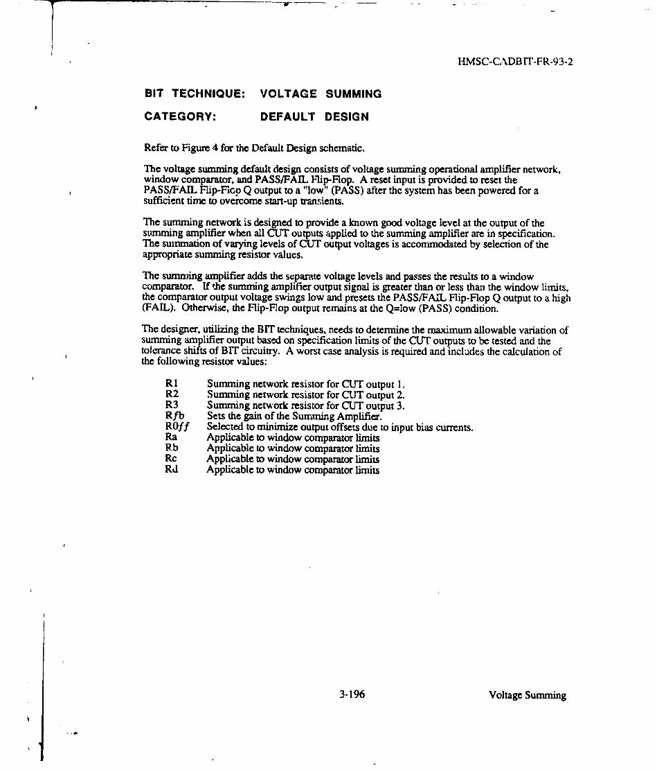
HMSC-CADBIT-FR-93-2
BIT TECHNIQUE: VOLTAGE SUMMING
CATEGORY: DEFAULT DESIGN
Refer to Figure 4 for the Default Design schematic.
The voltage summing default design consists of voltage summing operational amplifier network,window comparator, and PASS/FAIL Flip-Flop. A reset input is provided to reset thePASS/FAIL Flip-FIcp Q output to a "low" (PASS) after the system has been powered for asufficient time to overcome start-up transients.
The summing network is designed to provide a known good voltage level at the output of thestumnming amplifier when all CUT outputs applied to the summing amplifier are in specification.The summation of varying levels of CUT output voltages is accommodated by selection of theappropriate summing resistor values.
The summing amplifier adds the separate voltage levels and passes the results to a windowcomparator. If the summing amplifier output signal is greater than or less than the window limits,the comparator output voltage swings low and presets the PASS/FADL Flip-Flop Q output to a high(FAIL). Otherwise, the Flip-Flop output remains at the Q=low (PASS) condition.
The designer, utilizing the BIT techniques, needs to determine the maximum allowable variation ofsumming amplifier output based on specification limits of the CUT outputs to be tested and thetolerance shifts of BIT circuitry. A worst case analysis is required and includes the calculation ofthe following resistor values:
R1 Summing network resistor for CUT output 1.R2 Summing network resistor for CUT output 2.R3 Summing network resistor for CUT output 3.Rfb Sets the gain of the Summing Amplifier.ROff Selected to minimize output offsets due to input bias currents.Ra Applicable to window comparator limitsRb Applicable to window comparator limitsRc Applicable to window comparator limitsRd Applicable to window comparator limits
3-196 Voltage Summing

HMSC-CADBIT-FR 93-2
BIT TECHNIQUE: VOLTAGE SUMMING
CATEGORY: DEFAULT DESIGN, Contd
BASIC DESIGN EQUATIONS
wumine Amplifier Fquations:
VOUT= -RfbRn) + V2 + .... [1](R1 R2 Rn
ROFF Ri x ;2x ... Rnc Rib
RI + R2+.... Rn + Rfb (21
Where:
VI thruVn = CUT output voltages 1 thru nRI thru Rn = Summing resistor associated with CUT output voltages 1 thin n
Comarator Eouations:
VLTP = Rc+Rd +Vee [3]
(V +Vee [4]VUTP= Ra+Rb
Where:
VLTP = Voltage (lower trigger point)VUTP = Voltage (upper trigger point)VREF POS = Positive reference voltageVREF-NEG - Negative reference voltage
"• This BIT technique places a loading path between individual CUT outputs. The CUToutputs must be evaluated for compatibility with this technique.
• The summing amplifier output voltages must be limited to prevent exceeding thecomparator differential input voltage range (±5V) per LM 119.
"• As the number of CUT outputs are summed, the accuracy requirements increase for theBIT summing amplifier and window comparator. The ability to detect an out of tolerancecondition on each individual output, therefore, is reduced.
" Equa.' weighting factors for all CUT outputs may not be desirable for the summingnetwork in some cases. For example, equal weighting applied to the outputs of a tracking±15V power supply will not allow fault detection using this BIT technique. In this case, achange to apply unequal weighting will suffice.
3-197 Voltage Summing

HMSC-CADB IT-FR-93-2
-jl
cr-u..cnLL C\j
CL~
0 x
0 ca:-
+ +
4. 4.CD~i
C~j >>L nI ~ U)I
t - -I
UU
zS
c: UU.AAA-cc
3-9 Votg Sumn

HMSC-CADBrr-FR-93-2
Brr TECHNIQUE: VOLTAGE SUMMING
CATEGORY: BIT TECHNIQUE INSERTION DIAGRAM
Figure 5 shows the BIT Technique Insertion Diagram for this BIT technique.
BIT ELEMENT I
1. Connect the CUT analog outputs to the summing resistors RI thru R3 per the default designfigure 4.
2. Connect the summing resistors to the summing amplifier negative input per the default designfigure 4.
3. Crne¢#" i--istor5 ,ff and Rb, -ywcr, Pnd ground to the summming amnplifier per th!
default design figure 4.
BIT ELEMENT 2
1. Connect two LM1 19 comparators as a window comparator per the default design figure 4.
2. Connect the OP-07 amplifier output to the window comparator input per the default designfigure 4.
3. Connect resistors, power, and ground per the default design figure 4.
BIT ELEMENT 3
1. Connect the window comparator output to the PASS/FAIL flip-flop per the default designfigure 4.
2. Connect the reset input to the flip-flop.
3. Connect the PASS/FAIL output to the LRM out.
3-199 Voltage Summing

HMSC-CADBIT-FR-93-2
-w-0.i
U..U
p CLI_ __CL~ I-
rcU
cc -a
0 1
00
UAU
3-200 Voltage Sunmming

HMSC-CADB IT-FR-93-2
BIT TECHNIQUE: VOLTAGE SUMMING
CATEGORY: VARIABLE DEFINITIONS
Variable Variable Definition Units
v I. Number of CUT outputs to test none
CATEGORY: COMPONENT DETERMINATION EQUATIONS
The number of units (as represented by CAD symbols) and component parts (physical packages)
required to implement the Default Design are calculated as follows:
BIT Technique Parts Table (for Default Design)
Index, i Part Number Part Type T UTnits Required, ui--- 54ALS74A- FIP-FLOFP--
2 LM1l19 SELECTOR/MUX 2
3 OP-07 COUNTER I1
4 RNC55 BUFFER 2
5 RNC60 COB PARATOR Vj +6
The number of Component Parts Required is calculated (for i-th part) as follows:
ni = ceil ( ui / uppi)
Explanation of symbols used:
ni = Number of components (physical packages) required for i-th partui = Number of units (CAD symbols) required for i-th partuppi = Number of units/package for i-th part (from Table 4.0)ceil = Round up to nearest integer (e.g. 5.3 is rounded to 6)vi = User-supplied value for i-th variable (see Variable Definitions)
3-201 Veltage Summing

HMSC-C.A.DBIT-FR-93-2
BIT TECHNIQUE: VOLTAGE SUMMING
CATEGORY: PENALTY EQUATIONS
AREA (sq.in.) = Sum ( ni * ai ) + 15% for traces
WEIGHT (gins) = Sum ( ni * wi) + 10% for solder
POWER (mW) = Sum (ni * pi)
TEST TIME (ns) = 0
DELAY (ns) = 0
Explanation of Symbols Used.
Sum = Sum over parts in BIT Technique Parts Table (i=l to 5)ni = Number of component packages for i-th part in Parts Table
ni is calculated according to Component Deterraination Equationsai = Area in sq.in. of i-th part in Parts Tablepi = Power dissipation in mW (typical) for i-th part in Parts Tablewi = Weight in grams of i-th part in Parts Table
BIT TECHNIQUE: VOLTAGE SUMMING
CATEGORY: BIBLIOGRAPHY
None required.
3-202 Voltage Summing

14MSC-CADBIT-FR-93.2
REDUNDANCY
BIT TECHNIQUE DATA PACKAGE
CATEGORY: SHORT DESCRIPTION / DIAGRAMS
Redundant test techniques can be implemented on a concurrent basis by the design engineer as aBuilt-In-Test (BIT) tool. The approach taken is to include a Standard (also known as a goldendevice) on the Line Replaceable Module (LRM). The Standard is an electrical replica of the CircuitUnder Test (CUT) that requires BIT capability. The outputs from the CUYF and the $tandard arefed into a differential amplifier circuit which in turn feeds its output into a window comparator.The window comparator generates a FAIL signal if the differential output signal is either above apositive reference level or below a negative reference level.
Figures 1 and 2 show the Level I and 11 Block Diagrams for this BIT technique.
3-203 Redundancy

r - -- - -- - -. - -
IIMSC-CADBIT-FR-93-2
5L
J.I
L cc
3-204 Redur~dancy

HMSC-cAi)BII'.FR-93.. 2
000
:3:
2is
3-205 Redundancy

HMSC-CADBIT-FR-93-2
BIT TECHNIQUE: REDUNDANCY
CATEGORY: FLOW CHART / DESCRIPTION
Figure 3 shows the Flow Chart for this BIT technique.
!. Signals sent to the CUT are sent concurrently to a replica of the CUT (the Standard) during
opcration of the LRM.
2. The PASS/FARL Flip-Flop is reset to PASS.
3. Both the C1UT output and the output from the Standard are sent to a differential amplifierwhich provides an output which is proportional to the difference between the two signals.
4. The output of the differential amplifier is sent to the inputs of a window comparator wherethey arm compared to positive and negative reference voltages,
5. If the output of the differential amplifier is more positive or more negative than the referencevoltages, the PASS/FAIL Flip-Flop is set to FAIL. Otherwise, the Flip-Flop remains reset.
3-206 Redundancy
*1

HMSC-CADBIT-FR-93-2
CUT POWERED UP, INPUT STIMULIAPPUED TO CUT AND THE
REDUNDANT CIRCUIT (STANDARD)
RESETPASS/FAIL FF
TO PASS
OUTPUTS FROM CUT AND THESTANDARD ARE APPLIED TO A
DIFFERENTIAL AMPUFIER
THE OUTPUT OF THE DIFFEREN71ALAMPUIFIER IS SENT INTO AWINDOW COMPARATOR
WIDO OMARTR YS SET
DETECS ANPASS/FJULERROR? F TO FAIL
PASS/FAlL FFREMAINSRESET
TO PASS
274.844_100
Figure 3 BIT Sequence Flow Chart For Redundancy BIT Technique
3-207 Redundancy
HMSC-CADBIT-FR-93-2
BIT TECHNIQUE: REDUNDANCY
CATEGORY: ADVANTAGES
1. The technique operates concurrently with normal operation, therefore, no time is lost to testof the CUT.
2. All the circuit design must have been previously done for the CUT; therefore, it is readilyavailable for the Standard.
CATEGORY: DISADVANTAGES
1. In high frequency or critical timing applications, it may be difficult to synchronize the CUToutput signals with those of the redundant circuit.
2. Transient output changes of the CUT and the Standard may be difficult to test due to commonmode rejection and bandwidth limitations of the differential amplifier.
3. Large amounts of real estate will be consumed because the technique may double the circuitarea required.
4. For a largc number of CUT outputs, many differential amplifier and comparator BIT circuitswould be required.
3-208 Redundancy

HMSC-CADBIT-FR-93-2
BIT TECHNIQUE: REDUNDANCY
CATEGORY: ATTRIBUTES
1. CONCURRENCY
S'rest is concurrent with operational use.
2. TECHNOLOGY
0 Applicable to CUT circuits using analog technology.
3. CUT MICROPROCESSOR REQUIRED?
0 No.
4. CUT INTERNAL DESIGN REQUIRED?
' No.
5. AREA PENALTY
* The increase in area is proportional to the area of the CUT which is replicated plus the areaof the differential amplifier, window comparator, and PASS/FAL Flip-Flop.
6. WEIGHT PENALTY
* The increase in weight is proportional to the weight of the CUT which is replicated plusthe weight of the differential amplifier, window comparator, and PASS/FAIL Flip-Flop.
7. POWER PENALTY
• The increase in power is proportional to the power of the CUT which is replicated plus thepower of the differential amplifier, window comparator, and PASS/FARL Flip-Flop.
3-209 Redundancy

HMSC-CADBIT-FR-93-2
BIT TECHNIQUE: REDUNDANCY
CATEGORY: ATTRIBUTES, Contd
8. TIMING PENALTIES
Test Time
- The test time is negligible: It is equal to the sum of the delays due to the differentialamplifier, window comparator, and the PASS/FAIL Flip-Flop.
- If high frequency or critical timing specifications are required by the CUT, thendifficulties may arise when attempting to synchronize the CUTs output with the outputof the Standard.
- Throughput Delay
- No timing penalty is incurred with the use of this technique since it executesconcurrently with normal operation.
9. RELIABILITY IMPACT
With the use of this technique, failure rates increase proportionately to the circuit densityand complexity of the CUT. The failure rates for the differential amplifier, comparatorcircuit, and PASS/FAIL Flip-Flop must also be added to the total LRM failure rate.
10. CONCEPTUAL COMPLEX=IT
• Straightforward
11. HARDWARE/SOFTWARE/FIRMWARE
"* The hardware implementation requires a differential amplifier, window comparator,PASS/FAIL Flip-Flop, and a Standard. The Standard is an electrical replica of the CUT.
"* Software and Fuimware: Not applicable
12. DESIGN COST
" Hardware: Proportional to the cost of the Standard plus the differential amplifier, windowcomparator, and PASS/FAIL Flip-Flop.
" Software and Firmware: Not applicable
3-210 Redundancy

HMSC-CADBIT-FR-93-2
BIT TECHN!QUE: REDUNDANCY
CATEGORY: ATTiIBUTES, Contd
13. MEMORY REQUIREMENTS
• Not applicable
14. BIT CIRCUITRY SELF-TESTABLE?
Since the CUT is duplicated by the BIT circuitry, a failure in either the CUT or BITcircuitry is detectable, therefore, the majority of the circuitry added for a BIT is checkedout. Only the differential amplifier and window comparator circuits are not verifiedoperationally.
15. STAND-ALONE (SELF-CONTAINED) BIT?
• Yes.
16. NOTES
* None.
3-211 Redundancy

liMSC-CADBIT-FR-93-2
BIT TECHNIQUE: REDUNDANCY
CATEGORY: DEFAULT DESIGN
Refer to Figure 4 for the Default Design schematic.
The Redundancy BIT technique consists of a differential amplifier, window comparator,PASS/FAIL Flip-Flop, and a Standard; the latter is an electrical replica of the CUT. A reset inputis provided to reset the PASS/FAIL Flip-Flop output to a low (PASS) after the system has beenpowered for a sufficient time to overcome start-up transients.
The analog output signals from the CUT and Standard, which ideally are identical, are passed to adifferential amplifier. The differential amplifier amplifies the difference between the two signalsand passes the result to the window comparator. If the difference signal is greater than or less thanthe window limits, the comparator output voltage swings low and presets the PASS/FAIL Flip-Flop output to a high (fail). Otherwise, the Flip-Flop output remains at the low (PASS) condition.
The designer utilizing this BIT technique must determine the maximum allowable error betweenthe CUT and the Standard, and then calculate the necessary resistor values listed below:
RI Applicable to window comparator limitsR2 Applicable to window comparator limitsR3 Applicable to window comparator limitsR4 Sets the gain of the differential amplifier
3-212 Redundancy

HIMSC-CADBi'r-FR-.93-2
B1T TECHNIQUE: REDUNDANCY
CATEGORY: DEFAULT DESIGN, Contd
BASIC DESIGN EQUATIONS
Differential Amplier Eguations:
1Vo =AD [(VCUT - VSTD + Vio) + CMRR (V CM)] + V00 [1]CMRR
Where:
V0 = Output voltage of the differential amplifier (DA)AD = Differential gain of the DAVCjT = Output voltage of the CUTVSTD = Output voltage of the StandardVio = Input offset voltage of the DAV = Output offset voltage of the DACMRR = Common Mode Rejection Ratio of the DAVCM = Common Mode input voltage of the DA
R4= 4 Q [2]
G-1
Where:
G = Differential gain of the DAR4 = Feedback resistor in default design
3-213 Redundancy
L

HMSC.-CADBIT-FR-93-2
BIT TECHNIQUE: REDUNDANCY
CATEGORY: DEFAULT DESIGN, Coi~td
_C_9.mputo Euations:
VLTP = [(VREFPOS) - (VREFNEG)]R3 + VREFNEG [3]R1 + R2 + R3
[(VREFPOS) - (VREF NEG)](R2+R3) + VREFNEG [4]VUTP= RI +R24,R3
VLTP Voltage (lower trigger point)
VUTP = Voltage (upper trigger point)
Limitations
"Transient Response-The rate of change in the analog signals of the CUT and the Standardmust be considered in the BIT circuit design, e.g. a wider window limit may be necessarydue to the common mode rejection and bandwidth limitations of the differential amplifier.A worst case analysis is necessary.
"• This BIT technique adds loading to the CUT output, i.e. I100KO.
"* The differential amplifier output voltages must be limited to prevent exceeding thecomparator differential input voltage ransge (±5V) per LM 119.
3-214 Redundancy
HMSC-CAD~1T-FR-
2'OtJTPLI
c Ii 1 ~CUT._ANALOG-.OUT-
I NPUT -- __ _ * POP Slg Ul Va.... ll
S T A N D A R D SADM-NLGOTYlfIUT
FiESETC>-
Figure 4 Redufldafly - De'fauk De'igin
3-215/216 /* Re

HMSC-CAD13rT-FR-93-2
- - - --- ~OUTPUT
-7-
.1-s1
Ti
mulll
T N R DSTAORRO-ANALOG-OUT vpftFJwG
frgi 4 RcdwndaImcy - D~efault De-sigfl
3-21/216Redundancy

HMSC-CADBIU-FR-93-2
BIT TECHNIOUE: REDUNDANCY
CATEGORY: BIY 1ECHNIQUE INSERTION DIAGRAM
Figire 5 shows thre BIT Tecluique Insertin Diagrmn for this BIT technique.
BIT ELEMENT 1
1. Co-meet the CUT anaiog output to the AD524 differential amplifier positive input per thedefault design figure 4.
2. Connect the Standard analog output to the AD524 differential amplifier negative input per thedefault design figure 4.
3. Cunnect resistors, power, jumper, and ground to the ADD524 per the default design figure 4.
BIT ELEMENT 2
1. Connect two LM1 19 comparators as a window comparator per the default design figure 4.N
2. Connect the AD524 differential amplifier output to the window comparator hiput per thedefault design figure 4.
3. Connect resistors, power, jumper, and ground per the default design figure 4.
BIT ELEMEN' 3
1. Connect the window comparator output to the PASS/FAIL flip-flop per the default itsignfigure 4.
2. Connect the reset input to the flip-flop.
3. Connect the PASS/FAIL cutput to the LRM out.
3. '17 Redun~dancy j
HMSC-CADiBIT-FR-93-2
CC7u
3-1 Rdndc

HMSC-CADBrT-FR-93-2
BIT TECf*Q1IVE. REDUNDANCY
CATEGOHY: VARIABLE DEFINITIONS
Variable Variable Definition Units
v i. Number of 17LUT outputs to test none
v2. Board area of Standard for Redundancy BIT sq.in.
V3. Power (typical) of Stwidard for Redundancy BIT mW
V4. Wcight of Standard for Redundancy BIT gins
CATEGORY: COMPONENT DETERMINATION EQUATIONS
The numLxr of units (as represented by CAD symbols) and component parts (physical packagcs)
required to implement the Default Design are calf-ulatxi as follows:
BIT Technique Parts Table (for Oefault Design)
" ex]d Fxt "umber Part Type Units !tequired, uj"-'--"T" . .,54AI. 74A • -'"v1
2 LM119 C.OMPARATOR 2vj
3 AD524A DiFV AMPLIFIER vi4 RNR55 IF !TOR !______IRESISTO Svi
The number of Component Parts Required it, calculated (for i-th part) as Follows:
ni = ceil ( ui / upp)
Explanation of symbols used:
ni = Number of componens (physical packages) required for i-th partui = Number of units (CAD symbols) require.d for i-th partuppi = Number of units/package for i-th part (from Table 4.0)ceil = Round up to nearest integer (e.g. 5.3 is rounded to 6)Vi = User-supplied value for i-th variable (see Variable Definitions)
3-219 Redundancy

HMSC-CADBIT-FR-93-2
BIT TECHNIQUE: REDUNDANCY
CATEGORY: PENALTY EQUATIONS
AREA (sq.in.) = Sum ( ni * ai ) + 15% for traces
WEIGHT (gins) - Sum (lni * wi ) + 10% for solder
POWER (ioW) - Sum (ni * pi)
TEST TIME (ns) = 0
DELAY (ns) f 0
Explanation of Symbols Used.
Sum - Sum over parts in BIT Technique Parts Table (i=l to 4)ni = Number of component packages for i-th part in Parts Table
ni is calculated according to Component Determination Equationsai Area in sq.in. of i-th part in Parts Tablepi = Power dissipation in mW (typical) for i-th part in Parts Tablewi = Weight in grams of i-th part in Parts Table
CATEGORY: BIBLIOGRAPHY
None required.
3-220 Redundancy

HMSC-CADBIT-FR-93-2
ANALOG WRAPAROUND
BIT TECHNIQUE DATA PACKAGE
CATEGORY: SHORT DESCRIPTION / DIAGRAMS
Analog Wraparound is a non-concurrent Built-In-Test (BIT) Technique for systems employing ananalog input and output control structure, e.g. servo controllers, autopilot transceivers, and two-way communication links.
The Analog Wraparound technique consists of hardware and firmware in Read Only Memory[ROM] and specifically requires a microprocessor, some Digital-to-Analog (D/A) converters asoutput devices and some Analog-to-Digital (A/D) converters as input devices on board as part ofthe Circuit Under Test (CUT).
The technique consists of adding necessary circuitry so that upon a BIT INTIATE, the analogsignal leaving the D/A output devices can be routed to the A/D input devices on the LineReplaceable Module (LRM). An appropriate BIT routine is stored in ROM along with test data tocontrol the data transfer and compare the data received with the data transmitted. A mismatch willindicate a failure.
An option which the engineer may use to route the signal back to the microprocessor is to add ananalog switch to wrap the signal leaving the D/A through the switch, then to the A/D, and back to amicroprocessor.
Any analog command/responsc pair can be tested using the Analog Wraparound method.
The Microprocessor BIT technique (a related BIT technique) checks out the internal components ofthe microprocessor system. The analog wraparound BIT technique can be used to extend theMicroprocessor BIT to include the I/O.
Figures 1 and 2 show the Level I and II Block Diagrams for this BIT technique.
3-221 Analog Wraparound

HMSC-CADBIT-FR-93-2
-lm
ago
• .-e
10
3-222 Analog Wraparound

IfHMSC-CADBIT-FR-93-2
0
w 0
CL 0.
z0
41A
z za
3-223 Analog Wraparound

HMSC-CADBIT-FR-93-2
BIT TECHNIQUE: ANALOG WRAPAROUND
CATEGORY: FLOW CHART DESCRIPTION
Figure 3 shows the Flow Chart for this BI' technique.
1. A 'BIT INITIATE' signal is input from the LRM, so testing can begen.
2. Initialize the Circuit Under Test and set the Pass/Fail indicator equal to PASS.
3. Before applying a signal, enable the wraparound switches that are going to be used for thatparticular tes.
4. Apply the ROM test patterns to the D/A converter(s).
5. At this Ipint, the data is routed from the D/A convener through the proper enabledwraparound switches and into the A/D converter(s).
6. Delay and strobe. the memory chip to send the expected resuits to the microprocessor.
7. Microprocessor reads the results fiom the A/D converter(s) and compmvres it with the expectedresult from memory.
8. If comparison fails, set Pass/Fail to FAIL and end test. If comparison passes, continue.
9. if not the last ROM address, apply the next ROM test pattern and go back to STEP 5 andcontinue.
3-224 Anarlog Wrapakound
HMSC-CADBIT-FR-93-2
Q BIT NITIATI9
INITIAUZE CUTF -T PASSIFAIL INDICATORTO PASS
F SFLECT SWITCHES
IN ANALOG CHIPS
APPLY ROM TEST PATTERNS
TO /COVRE
ROUTE ANALOG SISNALTHRU ANALOG SWITCH TO
"A/D CONVERTER
DELAY & STI!ORE MEMORY CHIFTO SEND EXPECVTED RESULTS
TO MICROPROCESSOR I
MICROPROCESOR READS•ESULT FROM A/D CONVERTER
AND COMPARES WITH
APPLY EXPECTED RESULTNEXT ROM ..TEST PATTERN .
SNO SET"PAS 7PASS/FAIL
TO FAIL
274844.1 04
Figure 3 BiT Sequence Flow Chant For Anaiog Wraparound
3-225 Analog Wraparound
HMSC-CADBIT-FR-93-2
BIT TECHNIQUE., ANALOG WRAPAROUND
CATEGORY: ADVANTAGES
1. Analog wraparound only requires minimum hardware and is a conceptually simple
design which is easy to implement.
2. C(.ips that are needed are readily a'ailable.
3. This technique may also be used in conjunction with "MICROPROCESSOR BIT", anotherComputar-Aided Design'•Duilt-In-Test (CADB17) technique, to extend the BIT coverage toinclude the Input/Output (I/O) chips (which are not normally checked out with theMicroprocessor BIT).
4. Analog wraparuund provides a rigorous test of the A/D and D/A converter interfaces, e.g.:
a. Dynamic range
b. Analog accuracy
c. Conversion time
5. Test vectori can be wiitten to duplicate realistic application commands, e.g., step responseand waveform synthesis.
CATEGOSY: DISADVANTAGES
I. The technique only checks out a small portion of the LRM.
2. As the microprocessor system increases in size along with more D/A or A/D converters, thenthe number of analog switches must also increase (in quantity), therefore, increasing realestate and firmware requirements. Additional ROMs may be required to store the additionaltest patterns.
3-226 Analog Wraparound

HMSC-CADBIT-FR-93-2
BIT TECHNIQUE: ANALOG WIFAPAR-OUND
CATEGORY: ATTRIBUTES
1. CONCURRENCY
* Test is non-concurm-nt with oeraiioni use.
2. TECHNOLOGY
* Applicable to circuits using HYBRID teA,,mology, i.e. contains txA digital and andlogcircuitry resident in the CUT'.
3. CUT MICROPROCESSOR REQUIRED?
* Yes, the CUT must include a microprncessor und ROM space for dhe test vectors.
4. CUT INTERNAL DESIGN REQUIRED?
* Hardwarz - No.
- Firmware - Yes, the cur microprocessor ROM must be prograxmned with tsc vectors toimplement the wraparound BIT.
5. AREA PENALTY
* Minimal since most -iciroprocýsor LRMs have at most only a srnAll nu•nbcr of D/A orA/D peripheral devices.
6. WEIGHT PENALTY
• Increases as the number of analog chmannels are wrapped around.
7. POWER PENALTY
* Increases as the number of analog channels are wrapped around.
3-227 Analog Wraparound

HMSC-CADB IT-r-R-93-2
SIT TECHNIQUE: ANALOG WRAPAROUND
CATEGORY: ATTRIBUTES, Contd
8. TIMING PENALTY
0 Test Time - Increases as the number of test patterns are applied during test.
- Throughput delay - nreased to each analog channel due to the filtering effects of theanalog switch and buffers added in the analog signal path.
9. RELIABILITY IMPACT
- Decaeas basic reliability as the number of analog channels are wrapped around.
10. CONcF•YrUAL COMPWLE
• Straightforward.
II, HARDWARE.SGF0'WVARE/F1RMWARE
"* iHardware - For w-aparound switch and buffers.
- Software - No: applicabhc. The test vectors zre stored in the microprocessor ROM.
"• Firmware .- M'c roprocessor ROM is used for storage of test vectors.
12. DESIGN COST
- Hardware cost- Increases ,% the number of analog channels are wrapped around.
• Softvwre -- Not, applicable. The test vectors are all contained in the ROM
* Fhrmware cost- None, if all th, :est vectors fit within the available space of themicroprocessor.
13. MEMORY REQUIREMENTS
Increases as t~hc nurnter of test vectors are added.
i4. BIT CIRCUITRY SELF-TESTABLE?
* N,;.
15. STAND .,LONE (SELF-CONTAINED) Bfl-r'?
0 't es.
16. NOTES
* None.
3-228 Analog Wraparound

HMSC-CADBIT-FR-93-2
BIT TECHNIQUE: ANALOG WRAPAROUND
CATECORY: DEVAULT DESICN
Refer to Figue 4 for the Default Design schematic.
Thv CUT conasists of an 8751 microcontroller with A/ID and D/A ixiput and output interfaces. The8751 is used in the commercial industry for a wide variety of applications, e.g. microwave ovens,childrens' toys, and automotive dashboard and engine control electronics. The 8751 rontaixs allnecessary elements fer implemeniation of simple control systems without the. addition of RAM,ROM, or I/O interface logic. 128 byte RAM and 4K EPROM is resident on the chip as well as I/)port-, and interrupts.
"The A/D converter (US) is an 8 bit successive approximations type conve,'ter and accepts unipolar(0 to 5V) signals from the buffered output of the U5 operationai amplifier. The A/D converterprovides microprocessor compatibility with control pins for conversion execution (WR), tristatecontrol (CS), conversion completion statis (INTR), and 1 of 8 analog input channel selection(RD). The D/A conversion process is completed in 40 microseconds.
The U5 buffer amplifier incorporates a level shifting nctwork consisting of R5, R6, R7, and a 5volt refei-ence to convert the bipolar (± 5 volt) output of the LRM analog input to a unipolar (0 to 5volt) output range. A vassive Zener clamping network consisting ef VRI and R8 is also providedto motect the A/D cenverter (U38) input from over',oltage.
The D/A converter (U7) receives parallel 8 bit digitil words from port I cf the 8751 and is latchedto the D/A input wgis•e' via the 8751 port 3, bit 0. The D/A converter output voltage can swingover a bipoilar range (-5V to +5V). The output of the D/A converter is buffered with an operationalamplifier U4.
The Analog Wraparourd technique adds a wraparound analog switch (U2) and inp at/output bufferamplifies (Ul and U3). When the analog switch is selected in the normal mode (U2 pin AO), theLRM input and output analog signals flo•v, into and out of the curI via the analog switch. In thewraparound mode, the analog switch is activated and the CUT analog output is coupled back to theCUT analog input. The LRM an"log input and output lines are isolated from tie CUT when tlseanalog switch is selected in the wraparound mode. The BIT test is perfo-red by hiernicruprocessor which controls the analog switch condirion and the application of test vectors.
The BIT INITIATE is appljWl to port P3 bit 2 and the PASS/FAIL results are provided at port 4 bit4. lMe duradon aiA phasing of these signalc are defined in the microprocessor ROM and are at thediscretion of the user.
3-229 Analog Wraparound

HMSC-CADB %T-FR-93-2
BIT TECHNIQUE: ANALOG WRAPAROUND
CATEGORY- DEFAULT DESIGN, Contd
A notewthy limitation of the system includes the 300 ohm nominal series "on" resistance of theaalog switches. Conzideration must be made to reduce loading effects in the system by usage ofsuitable buffer amplifiers. In this case, the AD642 operational amplifier provides insignificantloading to the analog switch output and is satifdactory for demonstration of this BIT technique.
The user should also be aware that the analog switch, when selected in the wraparound mode,deadfaces &be analog input and analog outputs to the LRM. A closed loop control system will notbe suitabie here unless extra circuitry is added to force the LRM analog output to some fixed statewhile the Analog Wraparound BIT test is ptrformed.
Thc input voltage and bandwidth characteristics of the analog signal are limited by the filteringeffects of the AD642 buffer amp~ifier and analog switch.The Analog Devices Linear data bookshould be cons'ilted priir to usAge for any given application. No attempt is made here torecommend the specifv,, usage of these parts as a general solution to all Analog Wraparound BITimpltmentations.
3-230 Analog Wrap:around

TT
ANMAOG _IN A0642~
C i c uit Und -tr T est (C U T )-
Ii PG. 4-- S E
.10.1 -- I OKE50 e 2 FD 0
81 T _!NI TIA E ---- * 'I.. Nae'. A C IP I-- - -
-sms 5.1
1... 1
1 .L4 P #. 4 w - .- 84 v c r
as$ -- C LI15 - 010FO i vF
p 2 14Is :-! I I TRJ ± 6K
A0C0848 131O 71LpEigs = 1 T i V~ A.~ +.
_ _ _ _
__16
CRYSTL R 6AD1I4
______~30 30pFliu.~_
toFigureA4

HMSC-CAD~rrFp~92 .2
*i5V iv 15 v
WI I_SIA
! 0pF10 00PF _3 7FA
- 1 [ ~ DCOD1E LC9tC
4,5VSEELEC8
cc looL ilL_!1 b I I I_ 5 A A O U_ __ -
II IJage-tie ::eo A L.- --
10KRE 0064
U7 R34C3VINT1
844 + I _
T i '3a "U8 A -
S jll la Cd III0t,1:
__to of SAOh (KTAs C
14-NA4 if$Co I - V
P8 li p Is I
A Figunm 4 A.nalog Wzaparwl,, - Default Design
3-23 103' e21 Analog Wraparound

HMSC-CADBrr-FR-93-2
BIT TECHNIQUE: ANALOG WRAPAROUND
CATEGORY: SIT TECHNIQUE INSERTION DIAGRAM
Figure 5 Mhows the BIT Technique Insertion Diagram for this BIT techniq-,'e.
BlF ELEMNT. 1
k.onnwt thr CUT analog inut, output, and enable to the D(3509A per the default design figure 4.
Connect ,he LRM !N analog input and the LRM analog output to the AD6,42 btfffers per the defaultdesign figuire 4.
Connect resistors, capacitors, power, grounds, and jumpers to the AD642 buffers and DG509Aper the default design figure 4.
BIT ELE.MENT 2
Connect the LRM IN 'BIT INITIATE' to the CUT microprocessor input port.
BIT ELEMENT 3
Connnct the LRM CUT 'PASS/FAUl' to the CUT mimroprocessor output port.
3-233 Analog Wraparouad

HMSC-CADBIT-FR-93-2
ILISL-0I-
I I
' 1
SJ
CM
3-234 Analog Wraparound

HMSC-CADBrr-FR-93-2
BIT TECHNIQUE: ANALOG WRAPAROUNDCATEGORY: VARIABLE DEFINITIONS
Variable Variable Definition Units
vi. Number of CUT outputs to test none
v2. #Test patterns for Analog Wraparound BIT patterns
v3. Test pattern application rate for Analog Wrap BIT patterns/sec
V4. CUT initialization time sOc
CATEGORY: COMPONENT DETERMINATION EQUATIONS
The number of units (as represerted by CAD symbols) and component parts (physical packages)
required to implement the Default Design are calculated as follows:
BIT Technique Parts Table (for Default Design)
Index, i Part Numer..F Part Type Units Required, uiT -42 ' OP AMP (BUFFER) 2v
2 DG509A MUX, ANALOG v].
3 CKR22 CAPACITOR 3vj
4 RNR55 RESISTOR 3vi
The number of Component Parts Required is calculated (for i-th part) as follows:
ni = ceil ( ui / uppi)
Explanation of symbols used:
ni = Number of components (physical packages) required for i-th partui = Number of units (CAD symbols) required for i-th partuppi = Number of units/package for i-th part (from Table 4.0)ceil = Round up to nearest integer (e.g. 5.3 is rounded to 6)vi User-supplied value for i-th variable (see Variable Definitions)
3-235 Analog Wraparound

RMSC-CADBIT-FR-93-2
BIT TECHNIQUE: ANALOG WRAPAROUND
CATEGORY: PE14ALTY EQUATIONS
AREA (sq.in.) = Sum ( ni * ai) + 15% for traces
WEIGHT (gins) = Sum ( ni * wi ) + 10% for solder
POWER (mW) = Sum ( ni * pi)
TEST TIME (sec) = v4 + ( v2 / v3 ) + 0.000002
DELAY (ns) =. 2 * tBUFFER
Explanation of Symbols Used.
Sumn Sum over parts in BIT Techatique Parts Table (i=1f to 4)ni - Nwnber of component packages for i-th part in Parts Table
ni is calculated according to Component Deermination Equationsai = Area in sq.in. of i-th part in Parts TablePi = Power dissipation in mW (typical) for i-th part in Parts Tablewi = Weight in grams of i-th part in Parts Tablevi= User-supplied value for i-th variable (see Variable Definitions)tBUFFER = Max delay for OP AMP (BU-FFER) from Table 4.0
CATEGORY: DIBLIOGRAPHY
None r'qired.
3-236 Analog Wraparound
S. .. .. .. -.

HMSC-CADBIT-FR-93-2
4.0 MASTER PARTS DATA
Table 4.0 is a matrix that has a list of components and its attr•butes, It also provides the sourceswhere the attribute data is from. A iist of the amtiibutes and brief descriptions are shown below:
1. Component I.D.The number is used to identity the component.
2. Part NumberThis is the generic part number for the IC and style number for the resistor and capacitor.
3. Package TypeThe package type shows how many of the same device in a single package. It can be single,dual, octal, etc.
4. Part DescriptionThis is the part name with brief description of what the component is.
5. Units per PackageThis number indicates how many of the same device in a single package.
6. Number of Data BitsThis is the data width of the component when applicable.
'7. Number of Address Bits"This is the address width of the memory or microprocessor chip.
8. Number of PinsThis is the total number of physical pins on the component.
9. LengthThe length of the component is shown in inches.
10. WidthThe width oi' the component is shown in inches.
11. Area per PackageThe area of the package is calculated by multiplying the Length and Width of the component.The area is given in square inch.
12. Typical PowerThis is the typical dissipated power of the component shown in milliwatts.
13. Maximum PowerThis is the maximum dissipated power of the component shown in milliwatts.
14. Weight per PackageThis is the weight of the component package shown in grams.
4-1

HMSC-CADBIT- FR -93-2
15. Typical delayThis is the typical propagation delay from the device input to output.
16. Maximum delayThis is the maximum propagation delay from the device input to output.
17. Typical IcThis is the typical power supply current of the coripomnent in milliamps.
18. Maximum IccThis is the maximum power supply current of the component in miiliamps.
19. Nominal VCCThis is the nominal power supply voltage of the component in volts.
20. Maximum VCCThis is the maximum allowed power supply voltage of the component in volts.
21. ReferenceThe cohlmn shows the source of data extracted for this component. The pege gnumber and thetitle of the data book are provided.
4.1 PARTS/TECHNIQUE CROSS REFERENCE
Table 4.1 shows a list of components versus the BIT technique default designs using thosecomponents. To minimize the number of unique components, common technology and the samecomponents are used across the thirteen default designs as much as possibie.
4.2 QUESTIONS/TECHNIQUE CROSS REFERENCE
Table 4.2 is a matrix that has a list of questions versus the thirteen techniques using thosequcstions. In the CADBIT U1 software, the user is expected to answer a merged set of questionscorresponding to tle suitable BIT techniques. The answers to the questions are captured intovariables in the software and are used downstream in component detcrmination equations andpenalty equations.
4.3 SUITABILITY ATTRIBUTE DATA
The Suitability Selection Matrix (Figure 4.0) shows the criteria of determining suitable BITtechniques based upon the answers provided by the user to the four questions as part of the UserRequested Data. The selection process is performed by elimination of unsuitable techniques. Forexample, in order for analog wraparound to be a suitable technique, the CUT (Circuit Under Test)technology type is hybrid (H). In addition, the CUT allows non concurrent BIT technique, needsan available microprocessor, and doesn't care about the internal access constraint. T'he BITtechniques left are considered suitable techniques pending forced exclusion option by the user inthe selection process.
4-2

I 'NSC-CADBiT-FR-9?-2
U - - -
x > Z zz
Ixzt d6.
CL-1--J:
cc z"10~~ x > > 0It io'Iz j4>3

HMSC-CADBIT-FR-93-2
Pal NO
P111* 1
'~~1 I % Iq !~Ii P WIP; paai
C4 I -cm i;;pIq ' 9 1 1 l~pR I 4-14
4 , 3am i

HMSC-CADBIT.-FR-93-2
00
('3oI- 'C fi
YrL4 ~ ~w
:'-i ;LIAAS2Ii I-Iig
~ -~~ Tr I
4-5

HMSC-CADBIT-FR -93-2
co.
0 x( x
06-

HMSC-CADBIT-FR.93-2
5.0 MASTER SYMBOL LIST
Table 5.0 is a matrix that has a list of component symbols versus the corresponding componentlibrary where they locate. In the CADPJT H software, the mil.als_lib was selected for digitalcomponents mainly because of its availability dt the early release of Mentor Graphics 8.0. TheMentor spiceib contains basic comswonent types like resistor, capacitor etc. For moresophisticated analog components, Mentor accuparts lib is a good source. Logic AutomationIncorporated, an open door partner of Mentor Graphics provides SmartModel Library whichcontains specialized models for complex ICs such as microcontrollers and interface devices. Whena device does not exist in any of the available libraries, Mentor Graphics has application softwareallowing user to create symbol and build the corresponding model file to meet the deviceperformance.
5-1

HMSC-CADBIT-FR-93-2
XXX Xi
it
I- i-I -
cc~5 -
~1~X1
6:xxxxxixxxxx-: -. -1 __
5LC U,
uj Lu5-2
Uj1

HMSC-CADBrr-FR-93-2
6.0 BT TECHNIQUE LITERATURE" RESEARCH
A literature research wa,, conducted utilizing the reswurces of the GD corporate litvaraies and twomajor California Statp Universities. This literature search concentrated on testabiiiy and BITtcchniques described in the literature from 1986 to 199i. This restricted search was possible sincethe previous CADBIT program had performed a literature ;Parch prior to this period.
Over 250 articles and documents dealing with the latest BIT were idcntified from the abstracms,From these articles, 85 were selected, collected, reprinted, and distributed to GD test enginee•s.These engineers reviewed the data for two basic purposes. First, to identify additional BITtechniques that could be included in the BIT library; and second, to provide updated informaticnifor any of the 13 baselined techniques.
The breakdown of tM resuts of the lit-rature searuh by different BIT technique type is shown inFigure 6.0. The majority of the most recent articles dealt with some form of boundary scan andASICs. Some of the latest trends are described below:
PARTIAL SC.AN--Fartial scan is a variation cf full scaal technology. In practice, users can eitherstart with full scan and then remove dte more intrusive scan elcrnents to reduce penalty or launch anew design with less than one hundred percent scan. Growing numbers of design engineers favorpartial scan over full scan technology because it offers lower area overhead and less impact oncritical timing paths. With partial scan, carefully slected tecquential elements in an IC design aremiade controllable and observable by replacing them with scannable sequential ulements. ASICand IC designers nev"r like the area, power, and sp~ed overhead that comes with adding r~ip-flopsto every seeal scai chain in L circuit. An ASIC design where a 5% increase in area would require.the design t-2 rmove to another package si.-e and a high speed design that can afford very limitedtiming penalty i, r`ts critical path axe good cm.:didates for partial scan. As a vesult, partial scantechnology is prefe=ci by design application tightly constrained by area and perfonnancemequire-nents.
BOUNDARY SCAN-Boundary scan is still the best tool for improving the testability of printedcircuit boards. In pruatice, virtually all printed circuit boards designed with boundary scan devicftsalso contain conventional, non-scan parts. As long as this mix persists, test engineers will want toretain some in circuit test points even when boundary scan testing is used. The tough task,erspecially for complex high-pin-count boards, is deciding which test points shouid be kept andwhich can be dropped without sacrificing fault coverage. In this respect, bound.xy scan is stillevolving.
QUIESCENT CUJRRENT TEST-i (ddq) tcsting takes advantage of the CMOS property thatnormal standby current is miniscule but esalaies by orders of magnitude when defects are prcsent.The ideal circuit for I (ddq) testing is fully static 2nd fully complementary. This test will lead tofalse defect detection for fast dynamic logic, buses with unrh'iven states, pu! ups and pull-downs,and pre-change circuitry. I (ddq) testing takes into account the physical defect behavior in CMOSwhich other trditional stuck-at fault models lack. It appears that it may start to replace largeportions of functional and scan-test vector sequences.
ANALOG SCAN-Since analog signals are continuous, the scan approach is different from thedigital scan. One current approach is to insert test pins, control logic, and multiplexer cells into themixed signai ASIC during the design stage to make the test result observable. Analog scan de.sign
6-1

nIxMC-CADBI'-FP.-%.3-2
makes the hidden internal circuitry easily accessible for test. Cunrvni'y, mrjor effi.c in ,r.ting andsoftware development is trying to develop a similar stmidard to P[E1E E49. disit rd 3cM t Sstandard.
TESTABILITY35% -
TRENDS IN WIT TECHNIQUES AS A PERCEINT
3ENERAL OF "OTAL TZOCUMl•rS SURVE120.S~GENERAL
S25%- LOUIC
20%-
15%- PENT.... ,L.EXPE TI:: : L "' ' VHSIC
10%- • MEMORY SCAN MICAO-
5%- PROCESSOR
Figure 6.0 Litereture Research Resuhts And Tr'ids
All data from the iterature search were collected, reprinted, and stored in the CADBIT 9 te.hric,1data file. Additional documents, mainly from rezent magazine articles, were obtained ardreviewed throughout the program development. Relevmit articles were added to the tochni-J dacafiles and the CADBIT lt bibliography. At the end of the CADBIT II technical effort, more than 95articles have been filed.
The CADBIT 11 bibliogyaphy was compiled aid distributed at the First Technical InterfaceMeeting (TIM) and has been upiited throughout the prograw development.
6-2

.1' i *
' j, , #
'jig rdŽ1
Sf.1 1I1a' UI i z oA6 i
&weeCr\tnstcanltriil, omrwty In rh# eqnce (C31) actfNvit-s
P7A c klt bIatfOrms. :t af elected acqwAuc11n programs
s.ý%roora4k o j¶rL~ ktj~doal and ertfrerinq as4ýpcrt within
~ aras frcmpe~w~e ' tMe~to:,$ ProWam cf(9 s (POs) a#mWA thlr~ o~r4(t~to N;gfort' feo"'Ve Vaqts o of c hisers addition,
R~rn Mfltttyoo otiatgopy <44p4rtw otber AYM' Pumixt 101DbdSao~s, th2,
firFens uia crnsult c*w &Jthr OQ0 and nc-4)~inetRome
~ Ldt½~ZtRy aintatne tcWtieqZ carar~~c 1ýOpae t r.wwrch progravns in a',eas
OMumt -q"Ware prad&0~tA~ty, wi*e treev wirveiance' seWuS, slqgmvrl S
siAAP, .%o~4t statt~temf1potcs eltengltic eJhnoloqy, super-
cans~~t ~ty1 a~orruktubUym tar'it n etc ty
)It