![Chapter 1: Diode circuits vtusolutionvtusolution.in/uploads/9/9/9/3/99939970/analog_electronic[15ec32].pdf · Chapter 1: Diode circuits ... • Diode testing • Zener diode • Diode](https://static.fdocuments.in/doc/165x107/5aedefea7f8b9a9031905d54/chapter-1-diode-circuits-vt-15ec32pdfchapter-1-diode-circuits-diode.jpg)
gonuke.orggonuke.org/wp-content/toolkits/Electrical/electrical_1/... · Web viewApproximately 0.6...
70
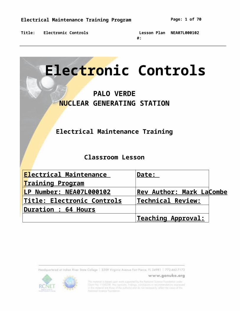
Electrical Maintenance Training Program Page: 1 of 70 Title: Electronic Controls Lesson Plan #: NEA07L000102 PALO VERDE NUCLEAR GENERATING STATION Electrical Maintenance Training Classroom Lesson Electrical Maintenance Training Program Date: LP Number: NEA07L000102 Rev Author: Mark LaCombe Title: Electronic Controls Technical Review: Duration : 64 Hours Teaching Approval: Electronic Controls
Transcript of gonuke.orggonuke.org/wp-content/toolkits/Electrical/electrical_1/... · Web viewApproximately 0.6...
Electrical Maintenance Training Program Page: 1 of 48
Title: Electronic Controls Lesson Plan #: NEA07L000102
PALO VERDENUCLEAR GENERATING STATION
Electrical Maintenance Training
Classroom Lesson
Electrical Maintenance Training Program Date: LP Number: NEA07L000102 Rev Author: Mark LaCombe Title: Electronic Controls Technical Review:Duration : 64 Hours
Teaching Approval:
Electronic Controls

Electrical Maintenance Training Program Page: 2 of 48
Title: Electronic Controls Lesson Plan #: NEA07L000102
INITIATING DOCUMENTS:Site Maintenance Training Program Description
REQUIRED TOPICS
NONE
CONTENT REFERENCES
Instruction Manual: 2445 Oscilloscope
Text: Solid State Fundamentals; Third Edition by Gary Rockis
Workbook: Solid State Fundamentals; Third Edition by James Donald & V. Douglas Browning
01DP-0IS13 ELEC. SAFE WORK PRACTICES
Textbook: Electronic Principles: Albert Paul Malvino PH.D, EE
Lesson Plan Revision Data
Jan 25, 2007 Mark Lacombe
Lesson plan revised...
Revised objectives (added/changed content) 1.1.1-1.1.9, 1.1.12-1.1.24
Enhanced enabling objective direction 1.1.6,1.1.8, 1.1.10, 1.1.11, 1.1.13, 1.1.15, 1.1.17, 1.1.19, 1.1.21, 1.1.24

Electrical Maintenance Training Program Page: 3 of 48
Title: Electronic Controls Lesson Plan #: NEA07L000102
Tasks and Topics Covered
The following tasks are covered in Electronic Controls:
Task or Topic Number*
Task Statement
Lesson: Electronic ControlsCTL10 Inspect and test circuit boardsCTL11 Check calibration and settings of electronic componentsCTL12 Test electronic componentsMTE01 Use Oscilloscope
Total tasks or topics: 4

Electrical Maintenance Training Program Page: 4 of 48
Title: Electronic Controls Lesson Plan #: NEA07L000102
TERMINAL OBJECTIVE: 1.1 Using reference material furnished by the instructor, the Plant Electrician will discuss solid state
fundamentals, build, calibrate and test electronic circuits to support theory, and demonstrate an understanding of solid state fundamentals by successful completion of a Lab Practical Evaluation (LPE).
1.1.1 Describe proper safe work practices and potential hazards working with associated Lab equipment and electronic components.
1.1.2 Describe the purpose for Inspecting and reworking printed circuit boards.
1.1.3 Describe the functions and associated controls of the Tektronix 2445 Oscilloscope.
1.1.4 Describe barrier potential effects on the PN junction of a general purpose diode.
1.1.5 Build/test/analyze a series and series-parallel diode circuit.
1.1.6 Describe special purpose diode design and application.
1.1.7 Build/test/analyze a Zener diode voltage regulator circuit.
1.1.8 Describe Single Phase DC power supply design and application.
1.1.9 Build/test/analyze a Single Phase DC Power supply circuit.
1.1.10 Describe voltage divider and voltage multiplier device design and application.
1.1.11 Describe Light Emitting Diodes (LED's) device design and application.
1.1.12 Build/test/analyze an LED circuit.
1.1.13 Describe Bipolar Junction Transistor (BJT) device design, operation and application.
1.1.14 Build/test/analyze a Bipolar Junction Transistor (BJT) switching circuit.
1.1.15 Describe Silicon Controlled Rectifier (SCR) device design and application.
1.1.16 Build/test/analyze an SCR switching circuit.
1.1.17 Describe Triac, Diac, and Unijunction Transistor (UJT) device design and application.
1.1.18 Build/test/analyze a Triac, Diac, and UJT circuit.
1.1.19 Describe Field Effect Transistor (FET) device design and application.
1.1.20 Build/test/analyze a Field Effect Transistor (FET) circuit.
1.1.21 Describe Integrated Circuit (Op Amp) device design and application.
1.1.22 Build/test/analyze integrated (Op Amp) circuits.
1.1.23 Describe Digital Logic symbols and truth tables.
1.1.24 Describe Fiber Optic circuit device design and application.

Electrical Maintenance Training Program Page: 5 of 48
Title: Electronic Controls Lesson Plan #: NEA07L000102
Lesson Introduction: Electronic Controls
The following items are things to consider in your Lesson Introduction. They are not mandatory.You should develop your own introduction and place that material in the Program Hierarchy in the Lesson Introduction Tab or appropriate Training Unit.
CLASSROOM GUIDELINES
If applicable, remind students of class guidelines as posted in the classroom. Pass the attendance sheet around and have it signed in Dark ink. Ensure that student materials needed for the class are available for each student. Emphasize student participation and remind them of your philosophy on asking and answering questions, if
applicable.
ATTENTION STEP
Give a brief statement or story to get student concentration focused on the lesson subject matter.
LESSON INTRODUCTION
Give a brief statement that introduces the specific lesson topic. Should be limited to a single statement.
MOTIVATION
Focus student's attention on the benefits they derive from the training. At Instructor's discretion. The need for motivation in each succeeding lesson must be analyzed by the Instructor and presented as necessary.
Instructor should include how the STAR process can be used to improve or enhance Operator Performance, if applicable.
Read and discuss lesson terminal objective and review lesson enabling objectives, if desired. If applicable, briefly preview the lesson topic outline and introduce the major points to be covered. The objective
review may have been sufficient. REINFORCE the following PVNGS management expectations as opportunities become available:
Nuclear SafetyIndustrial Safety PracticesSTAR and Self-CheckingProcedure ComplianceCommunication StandardsALARAPrevent Events
Electrical Maintenance Training Program Page: 6 of 48
Title: Electronic Controls Lesson Plan #: NEA07L000102
PURPOSE: This course presents a comprehensive overview for operation theory of semiconductor diodes, transistors, silicon controlled rectifiers (SCR's), operational amplifiers, light-activated components and the use of these solid state devices in practical circuit applications. This course also provides fundamental knowledge of electronics to support the performance of the associated objectives.

Electrical Maintenance Training Program Page: 7 of 48
Title: Electronic Controls Lesson Plan #: NEA07L000102
T.Obj 1.1 Using reference material furnished by the instructor, the Plant Electrician will discuss solid state fundamentals, build, calibrate and test electronic circuits to support theory, and demonstrate an understanding of solid state fundamentals by successful completion of a Lab Practical Evaluation (LPE).
1.1.1 Introduction
METHODS & ACTIVITIESSolid State Fundamentals by Gary Rockis is the text book used for this course. The following outline identifies the material to be covered.

Electrical Maintenance Training Program Page: 8 of 48
Title: Electronic Controls Lesson Plan #: NEA07L000102
EO 1.1.1 Describe proper safe work practices and potential hazards working with associated Lab equipment and electronic components.
1.1.1.1 Main Idea
Method & Activity: Chpt 1: Display PPT NEA07 & Solder Connections (Slides 1-8)
A. Electrical Safety:
1. Wear appropriate attire and render yourself non conductive (I.A.W. 01DP-0IS13) while performing lab activities. Gold and silver are excellent conductors of electricity.
2. You must wear safety glasses when working with lab experiments.
3. All students are encouraged to take a basic course in cardiopulmonary resuscitation (CPR) to aid a victim of electrical shock.
Method & Activity: Chpt 1: Figure 1-2 illustrates the corelation of current level and effect.
B. Electrical Shock:
1. A condition which results anytime the body becomes part of an electrical circuit.
2. Electrical shock effects vary from mild sensation, to paralysis, to death.
3. The severity of an electrical shock depends on the amount of electrical current in milliamps (mA) that flows through the body, the length of time the body is exposed to the current flow, the path the current takes through the body, and the physical size of the body through the current passes.
.

Electrical Maintenance Training Program Page: 9 of 48
Title: Electronic Controls Lesson Plan #: NEA07L000102
EO 1.1.2 Describe the purpose for Inspecting and reworking printed circuit boards.
1.1.2.1 Main Idea
Method & Activity: Inspect circuit board Traces, Foils, and Bus for Cold, Cracked or Recessed Solder Joints. Display PPT NEA07 and Solder Connection slides 12-24.
Electrostatic Discharge
Electrostatic discharge is the movement of electrons from a source to an object.
Static electricity is an electrical charge at rest.
The most common way to build static electricity is by friction.
Friction creates an electron buildup or a negative static charge.
When a person contacts a positive charged or grounded object, all excess electrons flow (jump) to that object.
Electrostatic discharge can be 35,000 volts or more.
People normally do not feel electrostatic discharges until the discharge reaches 3000 volts.
Solid state devices and circuits may be damaged or destroyed by a 10 volt electrostatic discharge. The effects of static discharges may be cumulative and not readily obvious.
Solid state devices and circuits may be damaged or destroyed by a 10 volt electrostatic discharge.
Prior to inspecting PC Boards, the technician or maintenance electricians should wear a wrist grounding strap or other type of grounding device to avoid damage to solid state devices and circuits.
B. The magnifying glass is used for solder inspections.
1. Inspect component lead solder connections to Pads, Traces, and Bus.
2. Inspect circuit board Edge Connectors for defects and/or degradation.
3. Inspect circuit boards for burnt or missing components.
4. Inspect circuit boards for defective/missing Molex Connector Pins.

Electrical Maintenance Training Program Page: 10 of 48
Title: Electronic Controls Lesson Plan #: NEA07L000102
EO 1.1.3 Describe the functions and associated controls of the Tektronix 2445 Oscilloscope.

Electrical Maintenance Training Program Page: 11 of 48
Title: Electronic Controls Lesson Plan #: NEA07L000102
1.1.3.1 Main Idea
Method & Activity: Have students read Instruction Manual 2445 section 3, Controls, Connectors & Indicators.
A. Tektronix 2445 Oscilloscope Measurement.1. The first thing to understand is that an oscilloscope is a volt meter. It does not measure
current, resistance, or watts.
2. The oscilloscope measures an amount of voltage during a period of time and produces a two-dimensional image.
B. Voltage Range Selection (VOLTS/DIV):1. The oscilloscope is divided into two main sections.
a. The voltage range selection switch VOLTS/DIV Switch on an oscilloscope selects volts per division instead of volts full scale used on a voltmeter.
b. The Voltage section: Voltage is measured on the vertical, or Y, axis of the display.
C. The Time Base Selection (SEC/DIV):
1. Time base is measured on the horizontal, or X, axis of the display.
2. The time base is calibrated in seconds per division and has range values from seconds to microseconds.
3. The time base controls the value of the divisions of the lines in the horizontal direction (X axis).
a. Example: If the time base is set to 20 μs (microseconds) per division, the trace will sweep the screen in 20 μs.
4. Measuring Frequency: a. The frequency (F) of an AC wave form can be found by dividing 1 by the time (T) it
takes to complete one cycle (F = 1/T). A cycle is one complete waveform.
b. To select frequency, press Delta V and Delta T at the same time
5. Attenuated Probes:
a. Most attenuated probes are 10 to 1.
b. An attenuated probe is used to permit higher voltage readings than are normally possible.
c. This means that if the voltage range switch is set for 5 V per division, using a 10 to 1 probe the display would actually indicate 50 V per division. If the voltage range switch is set to 2 V per division, the display would actually indicate 20 V per division.
Electrical Maintenance Training Program Page: 12 of 48
Title: Electronic Controls Lesson Plan #: NEA07L000102
D. Input Coupling Switches and Indicators – 1M ohm DC:
1. This allows both AC & DC signals to pass through the scope.
E. Channel 1 & 2 VOLTS/DIV Switches-
1. The VAR control must be in detent (fully clockwise) position to obtain a calibrated deflection factor.CHOP-OUT: ALT Switch – Chop (Latched in) to minimize waveform breaks when viewing repetitive signals to provide smoother sweep.
2. CHOP-OUT: ALT Switch selects the vertical display mode for multiple-channel displays.
3. Alt stands for alternate. This alternates the sweep between channel 1 & channel 2.
4. Chop: the chop mode alternates several times during one sweep. The chop mode is generally used when displaying two traces at the same time.
F. Delta V Switch-
1. Activates the Delta Volts measurement function. When pressed in, cancels any other Delta Measurement.
G. Delta T Switch-
1. Activates the Delta Time measurement function. When pressed in, cancels any other Delta Measurement.

Electrical Maintenance Training Program Page: 13 of 48
Title: Electronic Controls Lesson Plan #: NEA07L000102
EO 1.1.4 Describe barrier potential effects on the PN junction of a general purpose diode.
1.1.4.1 Main Idea
Method & Activity: Do exercises 3-1 through 3-3 in the workbook; Show Slides 25-31 (NEA07 & Solder Conn. ppt)
A. SEMICONDUCTOR Diodes:
1. Diodes are essentially solid-state semiconductor switches.
Method and Activity: Discuss mechanical check valve and fluid flow
2. Diodes are used extensively in electronics to allow or prevent current flow.
B. Electron flow: 1. In this text, current flow is based on electron theory which states that forward bias current
flows from negative to positive or cathode to anode.
2. Forward Bias:

Electrical Maintenance Training Program Page: 14 of 48
Title: Electronic Controls Lesson Plan #: NEA07L000102
a. Application of the proper polarity to a semiconductor diode is called forward bias voltage, or forward bias. Forward bias results in forward current which can range from a few milliamps to several hundred Amps based on the size and heat sink characteristics of the diode.
b. A diode has a relatively low resistance in the forward bias direction.
3. Depletion Region:
a. At the junction of the two materials, the P-Type and N-Type materials exchange carriers, creating a thin zone called the depletion region. Because the depletion region is very thin, it responds rapidly to voltage changes.
b. When voltage is applied to a diode in the forward direction, current will not flow until the depletion region is closed.
c. This voltage is called the forward breakover voltage. Only a few tenths of a volt is needed to bridge the depletion region.
1) Approximately 0.6 volts for a silicon diode and 0.3 volts for a germanium diode.
4. Reverse Bias:
a. When the opposite polarity is applied, it is called a reverse bias voltage, or reverse bias. Reverse bias results in reverse current which should be close to zero or very small – usually a millionth of an ampere (μ).
b. A diode has a considerably greater resistance in the reverse bias direction.
C. Diode Markings:1. Diodes are plainly marked with the schematic symbol, or there may be a black band at one
end of the diode to identify the cathode.
D. Understanding Semiconductor Materials:1. Diodes are made up of N-Type & P-Type materials by a process called doping.
a. The basic materials used in most semiconductor devices is either germanium or silicon.
b. In their natural state, germanium and silicon are pure crystals. These pure crystals do not have enough free electrons to support significant current flow. Thus their structure must be altered.
2. Doping is the process in which the crystal structure is altered. Atoms in the crystal are replaced with atoms from other elements to create more free electrons.
a. The addition of new atoms in the crystal creates N-Type & P-Type material.
b. Since electrons have a negative charge, the doped region is called the N-Type material.
c. The free electrons help move current and are called carriers.

Electrical Maintenance Training Program Page: 15 of 48
Title: Electronic Controls Lesson Plan #: NEA07L000102
d. Some of the elements commonly used for creating N-Type material are arsenic, bismuth, and antimony. The quantity of doping material used generally ranges from a few parts per billion to a few parts per million.
e. To create the P-Type material, a crystal is doped with atoms from an element that has fewer electrons in its outer shell that the natural crystal.
1) This combination creates empty spaces in the crystalline structure.
2) The missing electrons in the crystal structure are called holes. The holes are called positive charges.
3) Some of the elements commonly used for creating P-Type material are gallium, boron, and indium.
4) In the P-Type material the holes act as carriers. When voltage is applied, the holes are filled with free electrons as the free electrons move from negative potential to positive potential through the crystal.
E. Peak Inverse Voltage:1. Diodes are also rated for the maximum reverse bias voltage they can withstand. This rating
is called Peak Inverse Voltage (PIV).
2. The PIV ratings for most diodes used in industry range from a few volts to several thousand volts.
3. If the reverse bias applied to the diode exceeds the PIV rating, the diode will breakdown and pass current freely. Current passed in this manner is called avalanche current, which can destroy diodes.
4. To avoid avalanche, diodes with the correct rating must be used.
F. Testing Diodes:1. Test diodes using an ohmmeter to determine which end of the diode is the cathode and
which end is the anode.

Electrical Maintenance Training Program Page: 16 of 48
Title: Electronic Controls Lesson Plan #: NEA07L000102
EO 1.1.5 Build/test/analyze a series and series-parallel diode circuit.
1.1.5.1 Main Idea
Method & Activity: Perform exercise sequence 1 Objective 5 in the lab guide.
I. Electrical Safety:
1. Wear appropriate attire and render yourself non conductive (I.A.W. 01DP-0IS13) while performing lab activities. Gold and silver are excellent conductors of electricity
2. You must wear safety glasses when working with lab experiments.
II. Given a lab kit, build/test/analyze a series and series parallel diode circuit.
Electrical Maintenance Training Program Page: 17 of 48
Title: Electronic Controls Lesson Plan #: NEA07L000102
EO 1.1.6 Describe special purpose diode design and application.
1.1.6.1 Main Idea
Method & Activity: Perform exercise 3-4 in the workbook; Show Slides 32-37.
Describe Zener Diode Operation:
A. The Zener diode operates in the reverse breakdown region (reverse biased).
B. Zener resistance (rz) acts like a variable resistance.
C. Avalanche breakdown occurs when the Zener voltage is at or near the Zener breakdown voltage.
D. If a Zener is operating in either breakdown mode, the voltage across the Zener is essentially constant.
E. The terminal voltage (Vz) = Vz + Izrz, where Iz is the Zener current.
F. A Zener diode can be used to regulate a varying DC voltage. This is Line or Input Regulation.
G. A series-current-limiting resistor must be used in Zener diode applications. This resistor is in the circuit to provide the voltage drop difference between the Zener voltage and the source voltage.
H. Zener diodes come in a variety of ranges between 1.8 V and 200 V.
1. Zener diodes are also rated in their power-dissipating capacity or in their current-carrying limits.
2. For example: a Zener might be rated at 5.1 Volts and 1 Watt. Zener current would be Iz = 1 W/5.1 V = 196 mA.
3. 196 mA is the maximum current for this Zener diode and its rating is not to be exceeded.

Electrical Maintenance Training Program Page: 18 of 48
Title: Electronic Controls Lesson Plan #: NEA07L000102
EO 1.1.7 Build/test/analyze a Zener diode voltage regulator circuit.
1.1.7.1 Main Idea
Method & Activity: Perform exercise sequence 2 Objective 7 in the lab guide.
I. Electrical Safety:
1. Wear appropriate attire and render yourself non conductive (I.A.W. 01DP-0IS13) while performing lab activities. Gold and silver are excellent conductors of electricity.
2. You must wear safety glasses when working with lab experiments.
II. Given a lab kit, build/test/analyze a Zener diode voltage regulator circuit using an oscilloscope to determine circuit function.

Electrical Maintenance Training Program Page: 19 of 48
Title: Electronic Controls Lesson Plan #: NEA07L000102
EO 1.1.8 Describe Single Phase DC power supply design and application.

Electrical Maintenance Training Program Page: 20 of 48
Title: Electronic Controls Lesson Plan #: NEA07L000102
1.1.8.1 Main Idea
Method & Activity: Do exercises 4-1 and 4-2. show slides 38-39.
DC Power Supplies--Single Phase:Rectifiers:.
A. Half-Wave Rectifiers
1. If a diode is placed in a circuit with an AC source, the positive alternation will cause the diode to conduct and the negative alternation will turn off the diode. The result is a series of half-waves or pulsating DC current. This circuit is called a half-wave rectifier.
2. The average DC value of the output of a half-wave rectifier is found by VAVG = Vp X .637
3. The above formula neglects the effect of the forward voltage across a forward-biased diode. The actual value for the peak output voltage for the above formula is: Vp(out) = V(in) – 0.6 V. this is for a silicon diode.
4. The peak inverse voltage (PIV) for a rectifier diode is the maximum negative voltage that it must withstand in reverse bias.
5. Each diode has a PIV rating that must not be exceeded, or damage to the diode could result.
6. The output frequency of the half-wave rectifier is the same as the input frequency.
B. Full wave Rectifiers:
1. A center-tapped full–wave rectifier uses two diodes connected to a center-tapped transformer secondary. One diode conducts on the negative alternation and the other diode conducts on the positive alternation.
2. The average value for a center-tapped full-wave rectifier is twice the half-wave value. VAVG = 2Vp
X.637
3. A center-tapped full-wave rectifier diode must be selected to have a PIV greater than the secondary peak voltage.
C. Full-Wave Bridge Rectifier: 1. A full-wave bridge rectifier uses four diodes in a bridge circuit. This type of
rectifier does NOT require a center-tapped transformer.
2. The PIV rating of bridge rectifier diodes is half that of a center-tapped rectifier circuit.

Electrical Maintenance Training Program Page: 21 of 48
Title: Electronic Controls Lesson Plan #: NEA07L000102
3. The output frequency of the either type full-wave rectifier is twice that of the input frequency.
4. The output voltage of a bridge rectifier is equal to the transformer secondary voltage, if we neglect the diode voltage drops
2. AC and DC Voltage Measurements in Rectifier Circuits:Measurements in a rectifier circuit are generally taken with either a true RMS AC voltmeter
or an oscilloscope.
1. A DC voltmeter measures the average voltage (0.637 x Peak).
2. The AC voltmeter measures effective, or RMS (Root Mean Square)voltage (0.707 x Peak).
3. Avg Value is 90% of RMS
3. Power Supply FiltersA filter is required in a power supply to smooth the pulsating DC output.
A capacitor-input filter utilizes an electrolytic capacitor across the rectifier output.
The capacitor will produce an output that will have a small AC component called ripple voltage.
The ripple frequency equals the line frequency for a half-wave rectifier.
The ripple frequency equals twice the line frequency for either full-wave rectifier.
A filter capacitor should be as large as necessary to keep the ripple at a low value. If a very large capacitor is used, the diodes must be able to withstand the large initial surge current.
An inductor input filter uses an inductor in series with the line current to form an LC filter. This filter is very effective in reducing ripple.
Filters and Peak Inverse Voltage (PIV). Capacitive and Inductive filters will cause the PIV to increase and may require a diode with a higher PIV rating.

Electrical Maintenance Training Program Page: 22 of 48
Title: Electronic Controls Lesson Plan #: NEA07L000102
EO 1.1.9 Build/test/analyze a Single Phase DC Power supply circuit.
1.1.9.1 Main Idea
Method & Activity: Perform exercise sequence 3 Objective 9 in the lab guide.
I. Electrical Safety:
1. Wear appropriate attire and render yourself non conductive (I.A.W. 01DP-0IS13) while performing lab activities. Gold and silver are excellent conductors of electricity.
2. You must wear safety glasses when working with lab experiments.
II. Given a lab kit, build/test/analyze a Single-Phase DC Power Supply circuit using an oscilloscope to determine how capacitor filters affect circuit ripple voltage.

Electrical Maintenance Training Program Page: 23 of 48
Title: Electronic Controls Lesson Plan #: NEA07L000102
EO 1.1.10 Describe voltage divider and voltage multiplier device design and application.
1.1.10.1 Main Idea
Method & Activity: Do exercise 4-3; 5-1 & 5-2 in the workbook.
A. DC Power Supplies:1. Voltage Regulation:
a. A power supply whose output varies, depending upon changes of line voltage or load, is called an unregulated power supply.
b. A power supply that maintains a constant voltage across the output under various, conditions of line voltage load change is called a regulated power supply.
c. The voltage regulator is a variable resistance that automatically changes as the output voltage changes.
B. Voltage Divider:
1. Is a resistor, or a series of resistors, connected across the output of a power supply.
2. These resistors may be tapped at different points to provide a selection of output voltages.
3. The resistor, or a series of resistors, are in parallel with the various loads.
C. Voltage Multiplier:
1. A circuit designed to supply higher voltages with a limited load current.
2. The advantage of the voltage multiplier is its ability to develop voltages higher than the AC source without using a step-up transformer.
3. The voltage multiplier is often called a transformerless power supply.
4. It is capable of delivering a DC voltage as high as 400 volts from a 110-VAC source.

Electrical Maintenance Training Program Page: 24 of 48
Title: Electronic Controls Lesson Plan #: NEA07L000102
EO 1.1.11 Describe Light Emitting Diodes (LED's) device design and application.
1.1.11.1 Main Idea
Method & Activity: Do exercise 5-3 in the workbook; Show Slides 40-41.
A. LED’s: 1. Light Emitting Diodes:
a. An LED utilizes specifically doped semiconductor materials. The LED emits light when it is forward biased and electrons and holes are forced to recombine.
b. Although the device is a diode, the forward bias voltage is around 1.5 V to 2.4 V due to a larger manufactured depletion region. Kinetic energy released when electrons move across this region is visible light.
c. Alternate doping of impurities causes differing wavelengths of light and different colors are produced.
d. A typical current when conducting is about 20 mA.
e. Always us a series voltage dropping resistor in series with the LED to protect it from excessive current.
2. Light Emitting Diode Applications: a. Generally used for seven segment displays and status indicators.
EO 1.1.12 Build/test/analyze an LED circuit.
1.1.12.1 Main Idea
Method & Activity: Perform exercise sequence 4 Objective 12 in the lab guide.
I. Electrical Safety:
1. Wear appropriate attire and render yourself non conductive (I.A.W. 01DP-0IS13) while performing lab activities. Gold and silver are excellent conductors of electricity.
2. You must wear safety glasses when working with lab experiments.
II. Given a lab kit, build/test/analyze an LED circuit.

Electrical Maintenance Training Program Page: 25 of 48
Title: Electronic Controls Lesson Plan #: NEA07L000102
EO 1.1.13 Describe Bipolar Junction Transistor (BJT) device design, operation and application.

Electrical Maintenance Training Program Page: 26 of 48
Title: Electronic Controls Lesson Plan #: NEA07L000102
1.1.13.1 Main Idea
Method & Activity: Do exercise 6-1 thru 6-4 in the workbook; Show Slides 42-47.
I. Bipolar Transmitter Configuration, Operation and Circuit Analysis:
A. Transistors are used as amplification and switching devices in the electronics world.
1. They are considered bipolar because they utilize 2 differing polarities in their operation.
2. They are made up of 3 doped semiconductor parts: the emitter, the base and the collector.
a. The physical size of the "doped" area and the arrangement of the parts determine the type of transistor (NPN or PNP)
3. A bipolar junction transistor (BJT) is a semiconductor device with two pn junctions. In normal operation, the base emitter junction (BE) is forward-biased, while the base-collector junction (BC) is reverse-biased.
a. When base current (IB) is flowing across the BE junction and even though the BC junction is reverse-biased, then a current will flow from the emitter to the collector. This current is called collector current (IC).
b. The emitter current is the sum of these currents (IE = IB + IC.)
4. They operate in 4 distinct regions: Active, Cutoff, Saturation and Breakdown.
a. Active- normal region of operation including basic amplification. Also called linear region
b. Cutoff- used for switching. Cutoff is a condition in the operation of a bipolar junction transistor (BJT) when IB = 0 and therefore Ic= 0. In cutoff the BJT is acting like an open switch. No current is flowing.
c. Saturation- used for switching. At saturation the collector current becomes known as IC(sat) . Further increase in IB can cause no additional IC to flow. In saturation the BJT is acting like a closed switch. Maximum current is flowing.
d. Breakdown- never operate in this region. Transistor destruction will result
B. Transmitter circuit analysis
1. Gain or hfe or βDC: The ratio of the collector current IC to the base current IB is called the DC current gain or DC beta (βDC). βDC = IC
/ IE.
2. Characteristic curves can be used or derived to determine gain, load lines and Q points of transmitter operation.

Electrical Maintenance Training Program Page: 27 of 48
Title: Electronic Controls Lesson Plan #: NEA07L000102
a. The Load Line is determined via the two extremes of transistor operation (Saturation & Cutoff) and shows its max and min capabilities.
b. The Q-point or quiescent point is the point at which the transistor is in operation along the load line.
C. Transmitter Connections and Configurations
1. The three typical transmitter connections are: Common Emitter, Common Collector and Common Base.
a. Common Emitter- Most widely used. The emitter and ground side of each voltage source are tied together. The base current controls the collector current.
b. Common Collector- Collector tied to ac ground. Also called an emitter follower. The output directly follows the input. Collector voltage is the same as supply voltage Vcc.
C. Common Base- The input signal is fed into the emitter and the output signal is taken from the collector. The base is typically grounded via capacitor. Oscillator circuits.
D. Transistor Stability and Biasing
1. Thermal instability and subsequent runaway can destroy a transistor. Heat sinks, thermistors, diodes and Bias Stabilization circuits are typically used to prevent this from happening. There are three commonly used biasing circuits including Emitter feedback, Collector feedback and Combination bias.
a. Emitter Feedback utilizes a resistor on the Emitter circuit which will develop a larger positive (volt drop) as the current goes high (due to instability) which then opposes the base bias (reduces base current). Collector current will then follow and return to normal.
b. Collector Feedback utilizes a resistor to feed a portion of the output back to the input to return the circuit back to normal configuration. This type of feedback is also called negative feedback.
c. Combination Feedback utilizes both Emitter Feedback and Collector Feedback to stabilize a transistor.

Electrical Maintenance Training Program Page: 28 of 48
Title: Electronic Controls Lesson Plan #: NEA07L000102
EO 1.1.14 Build/test/analyze a Bipolar Junction Transistor (BJT) switching circuit.
1.1.14.1 Main Idea
Method & Activity: Perform exercise sequence 5 Objective 14 in the lab guide.
I. Electrical Safety:
1. Wear appropriate attire and render yourself non conductive (I.A.W. 01DP-0IS13) while performing lab activities. Gold and silver are excellent conductors of electricity.
2. You must wear safety glasses when working with lab experiments.
II. Given a lab kit, build/test/analyze a Bipolar Junction Transistor (BJT) circuit using an oscilloscope to determine circuit function.

Electrical Maintenance Training Program Page: 29 of 48
Title: Electronic Controls Lesson Plan #: NEA07L000102
EO 1.1.15 Describe Silicon Controlled Rectifier (SCR) device design and application.
1.1.15.1 Main Idea
Method & Activity: Do exercises 7-1 Thru 7-3 in the workbook; Do objective 11 in the lab guide; Show Slides 48-48.
A. Silicon Controlled Rectifier:
1. The silicon-controlled rectifier (SCR) is a four-layer device with three terminals. The terminals are identified as the Anode, Cathode, and Gate.
2. The SCR is placed in the circuit in the forward bias-position. The Anode (A) is positive with respect to the Cathode (K).
3. If the forward break over voltage is high enough, the SCR will conduct.
4. Normally, to turn an SCR on (or Fire it), a positive pulse is applied to the gate. The gate current IG, will allow the SCR to fire.
5. Once an SCR conducts, the only way to turn it off is to decrease the anode current below a value called the holding current (IH).
B. SCR Applications:
1. An SCR has many applications in the control of power.
2. In addition to being used in light dimmers, they are used in speed control of small ac motors, and more importantly, DC Motor Control Systems.
3. The SCR is used in industry to control power in Battery Chargers, Uninterruptible Power Supply Systems (UPS), Voltage Regulators and Variable Speed DC Drive Systems used in the Machine Tool Industry.
4. The SCR is also used as a power control element in welders and temperature control systems.
C. Testing an SCR:
1. Testing four-layer devices (SCR’s) is somewhat more difficult than testing transistors or diodes.
2. An ordinary 6 volt lantern is capable of gating on an SCR and also for checking both forward and reverse cathode leakage.

Electrical Maintenance Training Program Page: 30 of 48
Title: Electronic Controls Lesson Plan #: NEA07L000102
EO 1.1.16 Build/test/analyze an SCR switching circuit.
1.1.16.1 Main Idea
Method & Activity: Perform exercise sequence 4 Objective 12 in the lab guide.
I. Electrical Safety:
1. Wear appropriate attire and render yourself non conductive (I.A.W. 01DP-0IS13) while performing lab activities. Gold and silver are excellent conductors of electricity.
2. You must wear safety glasses when working with lab experiments.
II. Given a lab kit, build/test/analyze an Silicon Controlled Rectifier (SCR) ) circuit using an oscilloscope to determine circuit function.

Electrical Maintenance Training Program Page: 31 of 48
Title: Electronic Controls Lesson Plan #: NEA07L000102
EO 1.1.17 Describe Triac, Diac, and Unijunction Transistor (UJT) device design and application.

Electrical Maintenance Training Program Page: 32 of 48
Title: Electronic Controls Lesson Plan #: NEA07L000102
1.1.17.1 Main Idea
Method & Activity: Do exercises 8-1 Thru 8-2 in the workbook. Show Slides 48-51
I. TRIAC:Triac Construction, Operation & Application:
1. The Triac is a four-layer device with three terminals. The terminals are identified as T1, T2, and Gate(G).
2. The Triac is essentially two SCR’s back to back. There is only one gate terminal and two anode terminals.
3. A positive trigger pulse will trigger the Triac into conduction on either the positive or the negative alternation. If foreward (or reverse) voltage goes too high the device will turn on and conduct without a gate pulse. Can be considered an SCR for AC applications
4. The Triac is turned off by reducing the current below the holding value.
5. The Triac is more efficient than the SCR on AC because the Triac conducts on both alternations. This will deliver two times the power to the load. The power contained in the negative alternation is NOT wasted as it would be in an SCR application
6. Conduction time for the Triac can be easily controlled in a manner similar to the SCR.
7. Because of their versatility, Triacs are often used instead of mechanical switches. Also where amperage is low, Triacs are more economical than back-to-back SCR’s.
8. Triacs generally handle current less than 50 Amps.
B. Testing a Triac:
1. Special test equipment, such as an oscilloscope, is needed to test a Triac under operating conditions.
2. An ohmmeter can be used to make a rough test of the operating condition of a Triac.
II Diac:Diac Construction, Operation and Testing:
A Diac is a four-layer device that will conduct in both directions.
Conduction in the Diac will occur when the break over is reached. Either polarity will cause conduction.
3. A Diac is used primarily as a triggering device for gating on a Triac.
4. The gate-control circuits of Triacs can be improved by adding a break over device in the gate lead. The Diac is a breakover device.

Electrical Maintenance Training Program Page: 33 of 48
Title: Electronic Controls Lesson Plan #: NEA07L000102
5. The advantage of a Diac is that it delivers a pulse of gate current rather than a sinusoidal gate current.
B. Testing a Diac:An ohmmeter can be used to test a Diac for a short circuit.
If the Diac is good, the resistance will measure high in both directions.
Special test equipment, such as an oscilloscope, is needed to test a Diac if it is suspected to be open.
A Diac is essentially two Zener diodes connected back-to-back (Anodes connected together).
III. The Unijunction Transistor (UJT)UJT: Construction, Operation and Testing:
A UJT is a three-terminal device used to control current.
The unijunction transistor (UJT) consists of a bar of N-type material with a region of P-type material doped within the N-type material.
The N-type material functions as the base and has two leads, Base 1 (B1) and Base 2(B2).The lead extending from the P-type material is the emitter (E).In the symbol for the UJT, the emitter arrow points toward the base 1 (B1) terminal.
B. UJT Equivalent Circuit:The UJT can be considered a diode connected to a voltage divider network.
C. UJT Biasing:In normal operation, (B1) is negative, and a positive voltage is applies to (B2), and a positive
pulse is applied to forward bias the emitter.
D. Theory of Operation:When a positive pulse is applied to forward bias the emitter-B1 junction, the UJT will
conduct. The point of conduction (pulse) is a slightly higher voltage than the voltage that would be developed at the emitter junction (voltage divider). The device will continue to conduct until the emitter voltage is reduced to a value known as the valley point. The UJT will then shut off.
The action of the emitter-B1 resistance is much like that of a variable resistor R1, is normally higher that R2, but collapses to a very low resistance value when the emitter is in the forward bias condition.

Electrical Maintenance Training Program Page: 34 of 48
Title: Electronic Controls Lesson Plan #: NEA07L000102
E. UJT Applications:The UJT is used primarily as a triggering device because it generates a pulse used to fire
SCR’s and Triacs.
EO 1.1.18 Build/test/analyze a Triac, Diac, and UJT circuit.
1.1.18.1 Main Idea
Method & Activity: Perform exercise sequences 7-9, Objective 18 in the lab guide.
I. Electrical Safety:
1. Wear appropriate attire and render yourself non conductive (I.A.W. 01DP-0IS13) while performing lab activities. Gold and silver are excellent conductors of electricity.
2. You must wear safety glasses when working with lab experiments.
II. Given a lab kit, build/test/analyze a Triac circuit using an oscilloscope to determine circuit function.
III. Given a lab kit, build/test/analyze a Diac circuit using an oscilloscope to determine circuit function.
IV. Given a lab kit, build/test/analyze a Unijunction Transistor (UJT) circuit using an oscilloscope to determine circuit function.

Electrical Maintenance Training Program Page: 35 of 48
Title: Electronic Controls Lesson Plan #: NEA07L000102
EO 1.1.19 Describe Field Effect Transistor (FET) device design and application.

Electrical Maintenance Training Program Page: 36 of 48
Title: Electronic Controls Lesson Plan #: NEA07L000102
1.1.19.1 Main Idea
Method & Activity: Do exercise 10-1 & 10-2 in the workbook; Show Slides 53-62
Field-Effect Transistors (FET):
FET Types and Characteristics1. One type of Field Effect Transistor is the Junction Field Effect Transistor. (JFET) It is the most
common type of FET.
2. The other type of FET is the Metal-Oxide Semiconductor Field Effect Transistor (MOSFET).
3. There are two types of JFET’s. The N-channel and the P-channel. In both symbols there are the Gate (G), Source(S) and Drain (D). They are found in all FET's.
4. The input impedance of a JFET is very high (works great for multimeters).
5. The JFET operates as a voltage–controlled device and is controlled by the Gate-Source Voltage VGS. This voltage directly controls the drain current (ID).
B. JFET Biasing:
1. The JFET is a normally on device. It is biased so ID flows through the channel.
2. A JFET is always operated with the gate-source pn junction reverse-biased.
3. The JFET’s gate current IC is practically zero.
4. A JFET must be biased so that the pn junction between the gate and source is reverse-biased. This is easily accomplished by making VG = 0 V. The drain current will then produce a drop across the source resistor, RS. VGS will now be negative, thus biasing the pn junction correctly.
5. For an N-channel JFET, the value of VGS can be found by VGS = - IDRS when VG = 0 V.
6. To achieve linear operation, it is common to set the operating point at midway between the maximum and minimum drain current. ID = IDSS/2. This is called midpoint biasing.
7. A JFET must NEVER be forward biased. If the voltage applied to the gate source were forward biased, the drain current would increase to very high levels causing the input impedance to drop to a low value possibly destroying the device.
8. In an N-channel JFET, ID decreases as VGS becomes more negative because the channel becomes narrower. When VGS becomes more positive, ID increases. The value of VGS must remain negative to keep the gate-source junction reverse-biased.
9. The pinch-off voltage VP is the value of VDS where the channel becomes saturated and an increase in ID will not occur. The value of ID at pinch-off is called IDSS.

Electrical Maintenance Training Program Page: 37 of 48
Title: Electronic Controls Lesson Plan #: NEA07L000102
C. FET Circuit Configurations:
1. The JFET can be connected into three basic configurations: common-source, common-gate, and common-drain.
D. The Metal Oxide Semiconductor FET (MOSFET):
1. The MOSFET has a higher input resistance than the JFET.
2. The MOSFET is available in two modes, depletion (D) and enhancement (E).
E. MOSFET Theory of Operation:
1. The D-MOSFET can operate with either a positive or negative value of VGS.
2. A negative value of VGS operates the MOSFET in the depletion mode.
3. A positive value of Vgs operates the MOSFET in the enhancement mode.
4. The depletion mode acts as a capacitor with one plate as the gate and the other plate as the channel. As the gate becomes more negative, the channel is depleted of electrons. This causes ID to decrease.
5. The enhancement mode also acts as a capacitor, but as VGS becomes positive, electrons are attracted into the channel. This enhances the channel. As VGS increases, ID increases.
EO 1.1.20 Build/test/analyze a Field Effect Transistor (FET) circuit.
1.1.20.1 Main Idea
Method & Activity: Perform exercise sequence 10, Objective 20 in the lab guide.
I. Electrical Safety:
1. Wear appropriate attire and render yourself non conductive (I.A.W. 01DP-0IS13) while performing lab activities. Gold and silver are excellent conductors of electricity.
2. You must wear safety glasses when working with lab experiments.
II. Given a lab kit, build/test/analyze a Field Effect Transistor (FET) Amplifier circuit using an oscilloscope to determine circuit function.
Electrical Maintenance Training Program Page: 38 of 48
Title: Electronic Controls Lesson Plan #: NEA07L000102
EO 1.1.21 Describe Integrated Circuit (Op Amp) device design and application.

Electrical Maintenance Training Program Page: 39 of 48
Title: Electronic Controls Lesson Plan #: NEA07L000102
1.1.21.1 Main Idea
Method & Activity: Do exercise 11-1 in the workbook; Show Slides 63 – 79.
I. Integrated Circuit (IC) Advantages, Disadvantages and Operating Characteristics:
A. Advantages:1. They provide a complete circuit function in one small semiconductor package.
2. In addition to their small size and light weight, they are extremely reliable, consume less power, and cost less to operate than conventional components.
3. They generate less heat operate than conventional components and do not require as much cooling.
B. Disadvantages:
1. They are low power devices and are found mainly in the control circuit rather than in places where heavy currents are switched.
2. High voltages tend to break down IC’s.
3. They cannot be repaired. Therefore, when an IC fails or is damaged, it must be replaced.
C. Operational Amplifier:
1. One of the most widely used integrated circuits (ICs) is the Op amp.
2. An OP amp is a very high-gain, directly coupled amplifier that uses external feedback resistors and capacitors to control response characteristics.
3. Gains of 500,000 to 1,000,000 are common when selecting different feedback components and combinations.
4. OP amps are very versatile and can be used as a voltage follower, inverter, differentiator, integrator, adder, subtractor, or phase shifter.
D. Op Amp Characteristics:
1. Internally, an OP amp consists of three major parts:
a. A High-Impedance Differential Amplifier
b. A High-Gain Stage
c. Low-Output Impedance Power Output Stage

Electrical Maintenance Training Program Page: 40 of 48
Title: Electronic Controls Lesson Plan #: NEA07L000102
E. OP Amp Schematic Symbols:
Method and Activity: See Figure 11-12 on page 171 of the text.
1. The schematic symbols for op-amps may be shown in two ways. The standard op-amp symbol has two input terminals, called the inverting input (-) and the noninverting input (+), and one output.
F. Voltage Sources for Op Amps:The typical op-amp operates with two dc power supply voltages, one positive and the other
negative. Usually these two voltages are left off of the schematic symbol for simplicity but are always understood to be there.
Electrical Maintenance Training Program Page: 41 of 48
Title: Electronic Controls Lesson Plan #: NEA07L000102
EO 1.1.22 Build/test/analyze integrated (Op Amp) circuits.
1.1.22.1 Main Idea
Method & Activity: Perform exercise sequences 11- 20, Objective 22 in the lab guide.
I. Electrical Safety:
1. Wear appropriate attire and render yourself non conductive (I.A.W. 01DP-0IS13) while performing lab activities. Gold and silver are excellent conductors of electricity.
2. You must wear safety glasses when working with lab experiments.
II. Oscilloscope Settings:
A. Sets oscilloscope on correct coupling.
B. Sets function generator at correct frequency Adjusts AC input voltage to correct Peak to Peak voltage.
C. Use correct lead length (short).
D. Connects DC voltage for the Op Amp to correct polarity.
III. Given a lab kit, build/test/analyze an inverting op amp circuit using an oscilloscope to determine circuit function.
IV. Given a lab kit, build/test/analyze a non-inverting op amp circuit using an oscilloscope to determine circuit function.
V. Given a lab kit, build/test/analyze a Basic Comparator op amp circuit using an oscilloscope to determine circuit function.
VI. Given a lab kit, build/test/analyze a Timing Comparator op amp circuit using an oscilloscope to determine circuit function.
VII. Given a lab kit, build/test/analyze a Summing Amplifier circuit using an oscilloscope to determine circuit function.
VIII. Given a lab kit, build/test/analyze a Difference Amplifier circuit using an oscilloscope to determine circuit function.
IX. Given a lab kit, build/test/analyze a Single-Supply Integrator circuit using an oscilloscope to determine circuit function.
X. Given a lab kit, build/test/analyze a Dual-Supply Integrator circuit using an oscilloscope to determine circuit function.
XI. Given a lab kit, build/test/analyze a Single-Supply Differentiator circuit using an oscilloscope to determine circuit function.
XII. Given a lab kit, build/test/analyze a Dual-Supply Differentiator circuit using an oscilloscope to determine circuit function.
Electrical Maintenance Training Program Page: 42 of 48
Title: Electronic Controls Lesson Plan #: NEA07L000102
EO 1.1.23 Describe Digital Logic symbols and truth tables.

Electrical Maintenance Training Program Page: 43 of 48
Title: Electronic Controls Lesson Plan #: NEA07L000102
1.1.23.1 Main Idea
Method & Activity: Digital IC’s Do exercise 11-2 in the workbook; Show Slides 80-87.
I. Logic Symbols & Truth Tables:A. The AND Gate:
1. The AND Gate is a device with an output that is high only when both inputs are high.
2. Pins 1 & 2 are the input and pin 3 is the output.
3. A practical application would be an elevator control circuit. The elevator can’t move unless both the inner and outer doors are closed.
B. The OR Gate:
1. The OR Gate is a device with an output that is high if either or both inputs are high.
2. Pins 1 & 2 are the input and pin 3 is the output.
3. A practical application would be a burglar alarm circuit. If the front door or the back door are opened a signal is sent to the alarm circuit.
C. The NOR Gate:
1. The NOR Gate (Not OR) is a device with an output that is low if either or both inputs are high. Just the opposite of an OR Gate.
2. Pins 1 & 2 are the input and pin 3 is the output.
3. The small circle at the output of the NOR Gate symbol indicates an inversion of the output.
4. It is usually used in conjunction with other elements to implement more complex logic functions.
D. The NAND Gate:
1. The NAND Gate is a device with an output that is low only when both inputs are high. This is and inverted AND function.
2. Pins 1 & 2 are the input and pin 3 is the output.
3. The small circle at the output of the NAND Gate symbol indicates an inversion of the output.
E. The NOT Gate:
1. The NOT Gate is a device with an output that is low if the input is high or high if the input is low.

Electrical Maintenance Training Program Page: 44 of 48
Title: Electronic Controls Lesson Plan #: NEA07L000102
2. Example: The small circle at the output of the NAND Gate or NOR gate symbol indicates an inversion of the output (a NOT Gate).

Electrical Maintenance Training Program Page: 45 of 48
Title: Electronic Controls Lesson Plan #: NEA07L000102
EO 1.1.24 Describe Fiber Optic circuit device design and application.
1.1.24.1 Main Idea
Method & Activity: Do exercise 12-1 & 12-2 in the workbook; Show Slides 88-96.
I. Fiber Optics:A. Fiber Optic technology: uses a thin flexible glass or plastic optical fiber to transmit light.
1. Fiber optics is most commonly used as a transmission link. As a link, it connects two electronic circuits consisting of a transmitter and a receiver.
2. A single optical fiber has the same information-carrying capacity as a 900-pair of copper cable.
a. For Fiber Optics, the central part of a transmitter is its source.
b. The source consists of a light emitting diode (LED), infrared light emitting diode (ILED), or laser diode, which changes electrical signals into light signals.
c. The receiver usually contains a photodiode that converts light back into electrical signals.
d. The receiver output circuit also amplifies the signal and produces the desired results, such as voice transmission or video signals.
B. Light Emitting Diodes (LED's) and Infrared Emitting Diodes (IRED's):
1. LEDs: An LED is a PN junction diode that emits light when forward biased. The light emitted can be either invisible (infrared), or it can be light in the visible spectrum.
2. LEDs for electronic applications, due to the spectral response of silicon and efficiency considerations, are usually infrared emitting diodes (IRED).
3. LEDs are suitable for most applications requiring transmission distances up to several kilometers, and speeds up to several hundred megabits per second.
a. The LED is also more reliable, less expensive, and easier to use than the laser diode.
C. PIN Photodiodes:
1. The Photodiode has a small window to allow light to enter, which activates the PN junction. The operation of light radiation, when exposed to a PN junction, momentarily disturbs the structure of the PN junction. Thus, for the best response, light must be focused on the PN junction.
2. The disturbance is due to a hole created when a high-energy photon strikes the PN junction and causes an electron to be ejected from the junction. Thus, light creates electron-hole-pairs, which act as current carriers.

Electrical Maintenance Training Program Page: 46 of 48
Title: Electronic Controls Lesson Plan #: NEA07L000102
3. When connected in a circuit, the Pin Photodiode is placed in series with the bias voltage and connected in reverse bias which causes current to flow. The more light enters the more current flows.
4. Photodiodes conduct in only one direction.
5. Photodiodes have a high value of resistance when in the dark. As the light intensity increases, the internal resistance of the photodiode decreases.
D. Photo Transistors:
1. Photo Transistors: combine the effect of the photodiode and the switching capability of a transistor.
2. The advantage of Phototransistors have over photodiodes is that they have a sensitivity approximately 50 to 500 times greater.
3. The disadvantage of Phototransistors is that they are sensitive to changes in temperature and that protection against moisture is required.
E. Photo Darlington:
1. A multistage amplifier in one package. It works on the same principle that a single phototransistor does.
2. The driver transistor controls the follower transistor.
3. The Darlington configuration yields a high current gain, which results in a photodetector with verify high light sensitivity.
4. It has a low response to changes in light intensity.
F. LASCR's:
1. The schematic of an LASCR is identical to the schematic of a regular SCR. However, arrows are added in the LASCR schematic to indicate a light-sensitive diode.
2. When large current requirements are necessary, the LASCR can be used as a trigger circuit for a conventional SCR.
3. Like the photodiode, current is of a very low level in an LASCR. Even the largest LASCR is limited to a maximum of a few amps.
4. The primary advantage of an LASCR over a conventional SCR is its ability to provide isolation. Since the LASCR is triggered by light, the LASCR provides complete isolation between the input signal and the output load current.
G. Photo Triacs:
1. The Phototriac like, the SCR, can be triggered by light radiation of a specified density.
2. In darkness, the Triac is not triggered.

Electrical Maintenance Training Program Page: 47 of 48
Title: Electronic Controls Lesson Plan #: NEA07L000102
3. The Phototriac is bilateral and is designed to switch AC signals.
H. Optoelectronic Packaging:
1. Optoelectronics encompasses diodes, transistors, SCR’s, and Triacs.
2. Optoelectronic components require packaging that not only protects the chip, but also allows light to pass through the package to the chip. In other words it is a semiconductor package with a window.
I. Optocoupler (OPTOISOLATOR):
1. Internally, an Optocoupler consists of an infrared emitting diode (IRED) as the input stage and a silicon NPN phototransistor as an output stage.
2. The Optocoupler are used in situations where information must be transmitted between switching circuits that are electrically isolated from each other.
3. The Optocoupler is mostly used in applications where high voltage and noise isolation, as well as small size, are considerations.
4. The primary function of the Optocoupler is to provide electrical separation between input and output, especially in the presence of high voltages.

Electrical Maintenance Training Program Page: 48 of 48
Title: Electronic Controls Lesson Plan #: NEA07L000102
SUMMARY OF MAIN PRINCIPLESThe following items are things to consider in your lesson summary. They are not mandatory. You should develop your own summary.,
Objectives Review
Review the Lesson Objectives
Topic Review
Restate the main principles or ideas covered in the lesson. Relate key points to the objectives. Use a question and answer session with the objectives.
Questions and Answers
Oral questioning
Ask questions that implement the objectives. Discuss students answers as needed to ensure the objectives are being met.
Problem Areas
Review any problem areas discovered during the oral questioning, quiz, or previous tests, if applicable. Use this opportunity to solicit final questions from the students (last chance).
Concluding Statement
If not done in the previous step, review the motivational points that apply this lesson to students needs. If applicable, end with a statement leading to the next lesson.
You may also use this opportunity to address an impending exam or practical exercise.
Should be used as a transitional function to tie the relationship of this lesson to the next lesson. Should provide a note of finality.


