SIJRsijr.in/articles/Sahyadri-Journal-Research-Vol-2-Issue-2.pdf · Dr. Umesh M Bhushi (Principal)...
40
Sahyadri Journal of Research TM DECEMBER 2016 VOL.2 ISSUE 2 SIJR Journal Research Research Papers Review Papers Scientific Articles International ISSN 2456-186X
Transcript of SIJRsijr.in/articles/Sahyadri-Journal-Research-Vol-2-Issue-2.pdf · Dr. Umesh M Bhushi (Principal)...

Sahyadri Journal of Research
TM
DECEMBER 2016VOL.2 ISSUE 2
SIJRJournal
Research
Research Papers
Review Papers
Scientific Articles
International
ISSN 2456-186X

Advisors
Editorial Board
Members
Dr. D L Prabhakara (Director)
Dr. Manjappa Sarathi (Director-Consultancy)
Dr. Umesh M Bhushi (Principal)
Dr. Siddhartha.P.Duttagupta, IIT Bombay, Mumbai
Dr. Achanta Venu Gopal, TIFR, Mumbai
Dr. Shriganesh Prabhu, TIFR, Mumbai
Dr. Dinesh Kabra . IITB, Mumbai
Dr. Richard Pinto - Editor-in-Chief
Dr. Jayarama A - Editor
Dr. A. N. Prabhu, Dept. of Phy., MIT, Manipal
Mr. Arjun S. Rao (Dept. of ECE)
Mrs. Margaret D'Souza (Dept. of ECE)
Dr. Rathishchandra Gatti (Dept. of ME)
Dr. Ashwath Rao (Dept. of ECE)
Dr. Navin N. Bappalige (Dept. of Phy.)
Dr. Niraj Joshi ( )
Dr. Sarvesh Vishawakarma (Dept. of CSE)
Mr. Shamanth Rai (Dept. of CSE)
Mr. Harisha (Dept. of CSE)
Mr. Duddela Sai Prashanth (Dept. of CSE)
Mr. Vasudeva Rao P V (Dept. of CSE)
Mr. Naitik S T (Dept. of ISE)
Mr. Steven L Fernandes (Dept. of ECE)
Mr. Sunil Kumar (Dept. of Civil E)
Mr. Bharath Bhushan (Dept. of CSE)
Dept. of ECE
Disclaimer: The individual authors are solely responsible for
infringement, if any, of Intellectual Property Rights of third
parties. The views expressed are those of the authors. Facts
and opinions published in SIJR express solely the opinions of
the respective authors. Authors are responsible for citing of
sources and accuracy of references and bibliographies.
Although every effort will be made by the editorial board to
see that no inaccurate or misleading data, opinion or
statements appear in this journal, the data and opinions
appearing in the articles including editorials and
advertisements are the responsibility of the contributors
concerned. The editorial board accepts no liability
whatsoever for the consequences of any such inaccurate or
misleading data, information, opinion or statements.
Contents
SAHYADRI International Journal of Research | Vol 2 | Issue 2 | Dec 201626
Contents
Research / Review Articles
Scientific Articles
Editorial 27
Numerical Investigations of a Novel Sliding SupportCantilever Design for Vibration Energy Transduction 28-31
Design and implementation of high speed FIR filterusing CSD multiplier algorithm on FPGA's 32-35
Plane Stress Analysis of Layered Composite Platesubjected to varying in-plane patch load 36-40
Whispering Gallery Mode Resonators at Optical andTerahertz Frequencies: A Brief Review 41-50
Effects of Corrugation Profile on the Heat TransferRate of Fins 51-56
Study of Effect of Heat Treatment Processes OnMaterial Properties of Manganese Steels 57-61
Search for the value of ð - A brief history 62-63
General Guidelines 64
Vol. 2, Issue 2ISSN 2456-186X (Online)ISSN Pending (Print)
Mailing Address:Editor Sahyadri International Journal of ResearchSahyadri campus, Adyar, Mangalore - 575 007, IndiaE-mail: [email protected]: www.sijr.in
SAHYADRIInternational Journal of Research

Sahyadri International Journal of Research (ISSN: 2456-186X) is a journal covering
wide disciplines of science, engineering and technology. SIJR is published
biannually and is an open access journal available online.
It gives us immense pleasure to bring out Volume 2, Issue 2 of SIJR. However, there
are lots of challenges in bringing out a high quality research journal. Our focus is
multidisciplinary; the most important disciplines in which we would focus are
Physics, Chemistry, Applied mathematics, Electronics and Communication,
Mechanical Engineering, Civil Engineering and Computer Science and Engineering.
Apart from research papers, the journal also would publish articles on important
scientific discoveries. The current issue has research articles, review papers and a
scientific article.
Editorial team would like to thank the contributors and reviewers of
Volume 2, Issue 2.
- Editorial Board
Editorial
27SAHYADRI International Journal of Research | Vol 2 | Issue 2 | Dec 2016
Numerical Investigations of a Novel Sliding Support
Cantilever Design for Vibration Energy
TransductionR. Rathishchandra Gatti
Mechanical Engineering Dept., Sahyadri College of Engineering & Management, Adyar, Mangalore-575007
Email: [email protected]
AbstractCantilever topologies are very commonly used in energytransduction mechanisms which involved cyclic dynamicloads such as frequency tachometers for detecting thevibration frequency or energy harvesters for generatingenergy from wasted vibrations. Another advantage ofthe cantilever topology is its scalability to MEMS levelcompared to other spring structures such as helicaland leaf springs etc. The natural frequency of thecantilever depends on its length and this factor is utilizedhere to envisage a novel topology for construction ofenergy transducers. A numerical investigation using�nite element analysis is initially done to understandthe variation of the natural frequency with respect to thechanging length for a single cantilever beam. This is crossvalidated using analytical results.
Keywords: Cantilever, broadband, energytransduction, varying length, electromagnetic,piezoelectric, power harvesting, energy harvester, micro-electromechanical systems, biosensors, sensors.
1 Introduction
Recent advances in energy harvesting transducers andvibration sensors have necessitated the scientists totry for di�erent topological approaches to transducevibration energy into electrical energy [1]. Cantileverbeam structures are commonly used in convertingvibration energy to usable electrical energy such asthose found in piezoelectric vibration energy harvesters[2] and sensors such as Micro-electromechanical systems(MEMS)biosensors [3]. One of the key interests ofthe vibration energy harvesting research is the abilityof the energy harvesters to generate power for arange of frequencies for which several topologies havebeen investigated and reported. A few techniquesinclude frequency up-conversion [4], spatially varying themagnetic �eld [5], using non-linear oscillators [6] to namea few. This key design requirement of broadband energyharvesting is addressed in the proposed design.In the proposed design, a lumped mass single degree offreedom spring mass damper system is proposed wherethe spring is a cantilever �xed at one end and the lumpedmass suspended on the free end. The novelty in theproposed design is a sliding support or base that variesthe overhanging length of the cantilever thus leading to
the desired natural frequency. The inspiration for theproposed design is the design of Fullerton tachometerwherein the length of the suspended cantilever is adjustedby a screw in between the �xed structure and the free endwith lumped mass. Another inspiration for the proposeddesign are the promising results of the feasibility ofcreating sliding contacts in MEMS as discussed by IngridKu [7]. One important tribological design constraint isto minimize the frictional wear while designing slidingMEMS contacts since the surface friction coe�cient ishigh due to high surface to volume ratio in MEMSstructures. This can be minimised to acceptable levels ofµ = 0.05 to 0.1 for less than 100rpm by using low viscositylubricants such as Octadecylamine 0.1% in Silicon oil [7].
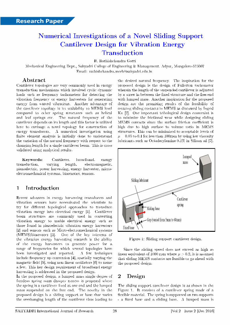
Figure 1: Sliding support cantilever design.
Since the sliding speed does not exceed as high aslinear equivalent of 1000 rpm where µ > 0.2, it is assumedthat sliding MEMS contacts are feasible to go ahead withthe proposed design.
2 Design
The sliding support cantilever design is as shown in theFigure 1. It consists of a cantilever spring made of a�exible material. The spring is supported on two supports- a �xed base and a sliding base. A lumped mass is
SAHYADRI International Journal of Research 28 |Vol 2| Issue 2 |Dec 2016|

suspended on the free end of the cantilever spring.
The natural frequency of the cantilever with free endsis given by,
fn =1
2π
√3EI
ml3(1)
where E = modulus of elasticity of the cantilever beam, I= mass moment of inertia, m = mass of the lumped masssuspended, l = overhanging length of the cantilever beam.In the proposed design, the length l can be varied byincreasing the gap between the �xed base and the slidingbase.Commonly available materials such as PET for cantileverspring, plain carbon steel for �xed and moving supportwere considered for the proposed mesoscopic design (atmm scale). At MEMS scale the choice of materials willde�nitely shift towards thin �lm polyamides and other�exible substrates for cantilevers and Silicon for lumpedmass, �xed support and moving supports for the ease offabrication. However, the scope of this study is limited tounderstand the dynamic behaviour and modal frequencyresponse of this unique design rather than identi�cation ofthe material selections for the MEMS fabrication whichcan be considered in the future work and therefore notin scope of this study. The main interest of designingany vibration energy harvester design is its ability toharvest energy over the range of frequencies from randomvibrations. Hence, linear dynamic FEA analysis withrandom base excitation load was performed to understandand know the modal frequencies of the cantilever atdi�erent varying lengths. In the FEA simulation, the gapbetween the �xed support and the moving support wasvaried from 5mm to 60 mm in steps of 5mm.
3 Simulation
3.1 Simulation Setup
Linear dynamic FEA analysis using random vibration wasperformed to understand and know the modal frequenciesof the cantilever at di�erent varying lengths. In the FEAsimulation, the gap between the �xed support and themoving support was varied from 5mm to 60 mm in stepsof 5mm at lab temperature of 25◦C.
3.2 Linear dynamic analysis simulation
conditions
The entire assembly was meshed using a solid mesh using8550 tetrahedral elements with element size of 1.652 mmand 14169 nodes as shown in Figure 2. The �xed baseand the sliding base was �xed using the �xed geometryconditions. A practical average value of 2mm amplitudewas considered for the base excitation load condition thatwas applied on the bottom surfaces of the �xed base andthe sliding base. The iterative solver namely the FFEPlussolver in Solid works was used rather than the accuratedirect sparse solver due to insu�cient memory space andlonger time required by direct sparse solver.
4 Results and Discussion
The energy transduction of the energy transducer dependson its amplitude of vibration. Also, the energy conversionis maximum when the prominent frequencies of the sourceof vibration are in resonance with the natural frequencyof the energy transducer. The proposed design considersvarying cantilever length and hence the modal frequenciesof the energy transducer will also need to be observed.Hence, the post processing of the simulation results wasdone to obtain the stress, displacement and the modalfrequencies from the linear dynamic FEA simulation.
Figure 2: Finite element Mesh using Solid mesh.
4.1 Stress and Displacement results
For the design to be safe, the distortion energy theoryand hence, the Von-Mises stress analysis was considered.As seen in Figure 3, the Von-Mises stress was found tobe maximum at 0.0377N/m2 and was within the limitsof yield point of the cantilever spring. This was becausethe base displacement of 2mm was too low for inducingany high stresses at the stress zones. It was also becauseof the high yield strength of Plain carbon steel that waschosen for the cantilever spring.
As evident in Figure 4, the displacement of the tipof the mass was maximum. The maximum displacementof the cantilever beam is found to vary from 1.23 mmfor 60mm gap to 5.76 mm for 5mm gap. The mass tipexcitation to the base excitation magni�cation ratio wasthus 1.23/2 = 0.615 for 60mm gap and 5.76/2 = 2.88 for5 mm gap. This is true since the length of the overhang ofthe cantilever decreases with the increase of gap. The topdown approach of the energy harvester design would beto estimate the amplitude of vibration required and thendesign the sliding base energy harvester to appropriaterange of length variations.
SAHYADRI International Journal of Research 29 |Vol 2| Issue 2 |Dec 2016|
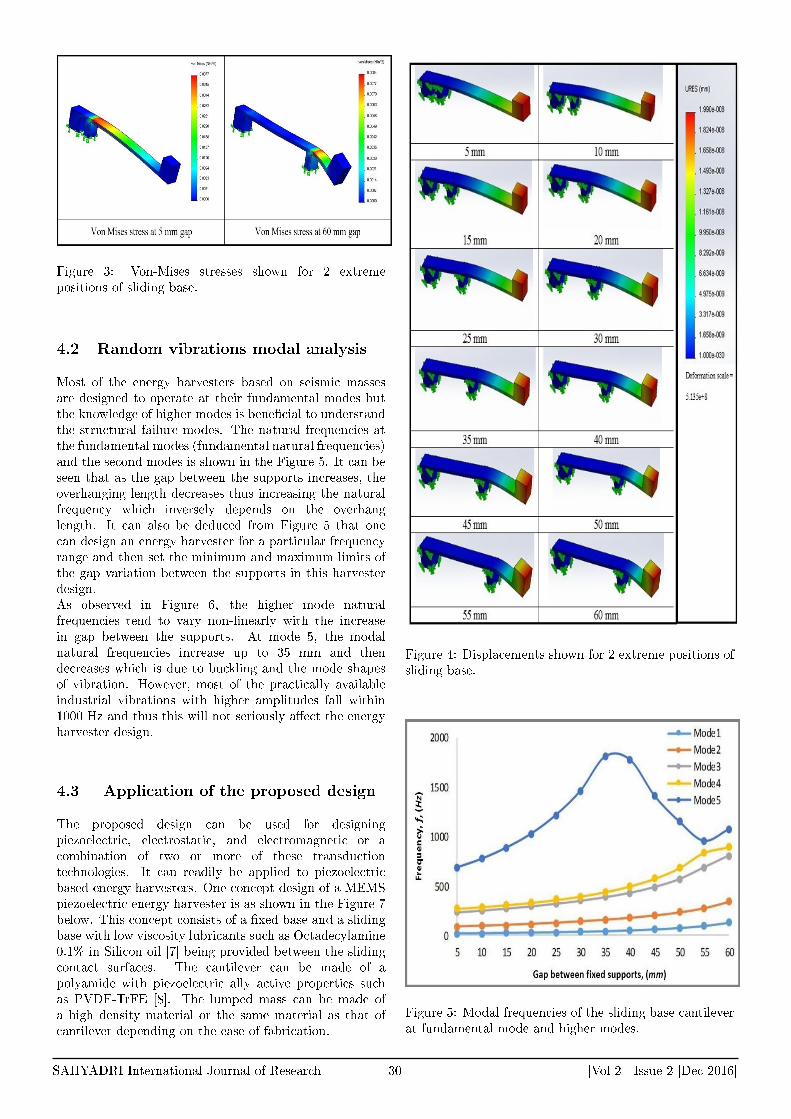
Figure 3: Von-Mises stresses shown for 2 extremepositions of sliding base.
4.2 Random vibrations modal analysis
Most of the energy harvesters based on seismic massesare designed to operate at their fundamental modes butthe knowledge of higher modes is bene�cial to understandthe structural failure modes. The natural frequencies atthe fundamental modes (fundamental natural frequencies)and the second modes is shown in the Figure 5. It can beseen that as the gap between the supports increases, theoverhanging length decreases thus increasing the naturalfrequency which inversely depends on the overhanglength. It can also be deduced from Figure 5 that onecan design an energy harvester for a particular frequencyrange and then set the minimum and maximum limits ofthe gap variation between the supports in this harvesterdesign.As observed in Figure 6, the higher mode naturalfrequencies tend to vary non-linearly with the increasein gap between the supports. At mode 5, the modalnatural frequencies increase up to 35 mm and thendecreases which is due to buckling and the mode shapesof vibration. However, most of the practically availableindustrial vibrations with higher amplitudes fall within1000 Hz and thus this will not seriously a�ect the energyharvester design.
4.3 Application of the proposed design
The proposed design can be used for designingpiezoelectric, electrostatic, and electromagnetic or acombination of two or more of these transductiontechnologies. It can readily be applied to piezoelectricbased energy harvesters. One concept design of a MEMSpiezoelectric energy harvester is as shown in the Figure 7below. This concept consists of a �xed base and a slidingbase with low viscosity lubricants such as Octadecylamine0.1% in Silicon oil [7] being provided between the slidingcontact surfaces. The cantilever can be made of apolyamide with piezoelectric ally active properties suchas PVDF-TrFE [8]. The lumped mass can be made ofa high density material or the same material as that ofcantilever depending on the ease of fabrication.
Figure 4: Displacements shown for 2 extreme positions ofsliding base.
Figure 5: Modal frequencies of the sliding base cantileverat fundamental mode and higher modes.
SAHYADRI International Journal of Research 30 |Vol 2| Issue 2 |Dec 2016|
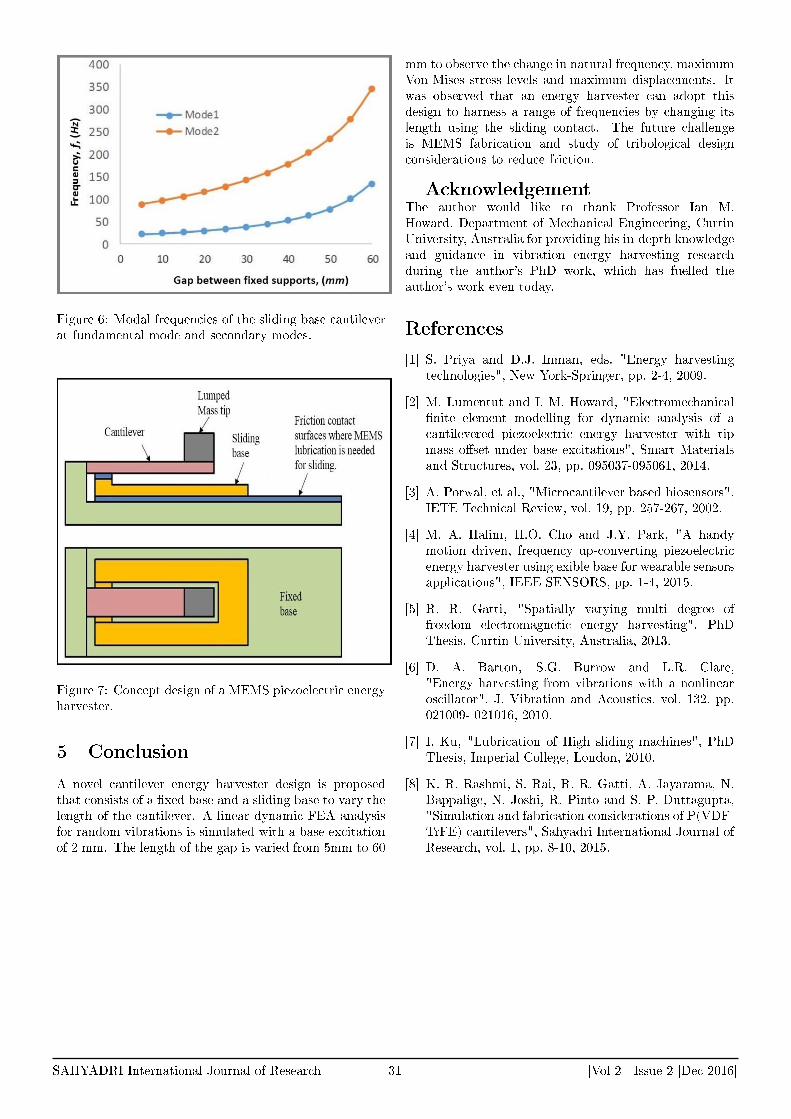
Figure 6: Modal frequencies of the sliding base cantileverat fundamental mode and secondary modes.
Figure 7: Concept design of a MEMS piezoelectric energyharvester.
5 Conclusion
A novel cantilever energy harvester design is proposedthat consists of a �xed base and a sliding base to vary thelength of the cantilever. A linear dynamic FEA analysisfor random vibrations is simulated with a base excitationof 2 mm. The length of the gap is varied from 5mm to 60
mm to observe the change in natural frequency, maximumVon-Mises stress levels and maximum displacements. Itwas observed that an energy harvester can adopt thisdesign to harness a range of frequencies by changing itslength using the sliding contact. The future challengeis MEMS fabrication and study of tribological designconsiderations to reduce friction.
AcknowledgementThe author would like to thank Professor Ian M.Howard, Department of Mechanical Engineering, CurtinUniversity, Australia for providing his in-depth knowledgeand guidance in vibration energy harvesting researchduring the author's PhD work, which has fuelled theauthor's work even today.
References
[1] S. Priya and D.J. Inman, eds. "Energy harvestingtechnologies", New York-Springer, pp. 2-4, 2009.
[2] M. Lumentut and I. M. Howard, "Electromechanical�nite element modelling for dynamic analysis of acantilevered piezoelectric energy harvester with tipmass o�set under base excitations", Smart Materialsand Structures, vol. 23, pp. 095037-095061, 2014.
[3] A. Porwal, et al., "Microcantilever based biosensors",IETE Technical Review, vol. 19, pp. 257-267, 2002.
[4] M. A. Halim, H.O. Cho and J.Y. Park, "A handymotion driven, frequency up-converting piezoelectricenergy harvester using exible base for wearable sensorsapplications", IEEE SENSORS, pp. 1-4, 2015.
[5] R. R. Gatti, "Spatially varying multi degree offreedom electromagnetic energy harvesting", PhDThesis, Curtin University, Australia, 2013.
[6] D. A. Barton, S.G. Burrow and L.R. Clare,"Energy harvesting from vibrations with a nonlinearoscillator", J. Vibration and Acoustics, vol. 132, pp.021009- 021016, 2010.
[7] I. Ku, "Lubrication of High sliding machines", PhDThesis, Imperial College, London, 2010.
[8] K. R. Rashmi, S. Rai, R. R. Gatti, A. Jayarama, N.Bappalige, N. Joshi, R. Pinto and S. P. Duttagupta,"Simulation and fabrication considerations of P(VDF-TrFE) cantilevers", Sahyadri International Journal ofResearch, vol. 1, pp. 8-10, 2015.
SAHYADRI International Journal of Research 31 |Vol 2| Issue 2 |Dec 2016|
Design and implementation of high speed FIR �lter
using CSD multiplier algorithm on FPGA'sG. K. Dayanand1∗, A. Jayarama2 and C. Shantharama Rai3
1E & C Dept., Canara Engineering College, Mangalore, 574219 India
2Physics Dept., Sahyadri College of Engineering and Management, Adyar, Mangalore, 575007 India.
3E&C Dept., AJIET, Mangalore, 570006 India.
∗Email: [email protected]
Abstract
A Canonic Signed Digit(CSD) algorithm for Finite Im-pulse Response (FIR) �lters is designed and simulated inVery High Speed Integrated Circuit Hardware Descrip-tion Language (VHSIC-HDL) and implemented on Spar-tan 2E Field-Programmable Gate Array (FPGA). Thecustomized Integrated Circuit (IC) can be used as a po-tential high speed FIR �lter for various applications in the�eld of satellite, mobile communication etc. The designedFIR �lter consumes total memory of 75320 Kilobytes withfrequency of 146.370MHz in Xilinx Sparten 2E kit
Keywords: FPGA, CSD , FIR Filter, VHDL.
1 Introduction
The modern technology is moving towards high speedspeech processing, image compressing, digital modulationtechniques which involve processing of digital signals andapplications like optical �ber or wireless communication.The processing, compression and modulation of digitalsignal should be very fast, so that higher speed transmis-sion can be possible [1, 2].
Digital signals can be stored and removed, transmit-ted and received, processed and manipulated, all virtuallywithout error. Two major advantages that distinguishDSP from other application oriented general purpose com-putation processing are the real-time throughput, speedand data driven property. DSP �lters are signal condition-ers. Finite Impulse Response (FIR) digital �lters, widelyused in signal processing , are one of two primary types ofdigital �lters used in digital signal applications; the othertype is feedback oriented In�nite Impulse Response �lter(IIR).
Digital �lters can be implemented with less hardwareusing a CSD representation. For multipliers computa-tion is commonly done by addition and shift methods.In CSD method, number of additions and shifts opera-tions implemented for a multiplier depends on the num-ber of non-zero binary bits in the binary digits representa-tion. Extracting common sub-computations between the�lter coe�cients can minimize the number of additionsand shift operations [3, 4]. This realizes an area-e�cientimplementation of the �lter. Coe�cient transform arevery important in realizing area-e�cient multiplier. Byapplying coe�cient transform in combination with sub-expression and pre-computation technique, we can save
many additions and subtractions. Strength reduction atthe algorithm level can be used to reduce the number ofadditions. An e�cient algorithm is represented by thereduced �nite digital �lter coe�cients, which are repre-sented by a Canonical Signed Digits numbers representa-tion, i.e., numbers represented as sums or subtraction ofpower-of-two [5].
Recent interest is in using minimum adder/subtracterunits for multiplier. The design and implementation ofdigital �lters has extensively contributed to future devel-opment using CSD number system [6,7]. The integer cod-ing schemes considered here belong to a class of numberscalled �xed point. Fixed point refers to the fact that thebinary point is found in �xed location. There exist a fewother �xed point systems, which hold some interest to thedigital signal processing scientists. One of such system iscalled the canonical signed digit code. In the early 1950's,this code enjoyed a high degree of popularity.
A common method of carrying out multiplication isby addition and shifting operations of constant numbers.By optimized hardware utilization, it is possible to al-ter this method by addition or subtractions. The CSDmethod has the bene�ts of reducing the number of ad-ditions/subtractions, in addition to e�ortlessly handlingnegative multipliers; results are obtained by represent-ing the multiplier in CSD form. In this paper we re-port, design of high-speed computation FIR �lters usingCSD based multiplier implemented on FPGA's for DSPapplications. DSP systems can be realized using pro-grammable processors or custom designed hardware cir-cuits fabricated using very large scale integration (VLSI)circuit technology.
1.1 CSD algorithm
An algorithm for computing the CSD format of a W-bitnumber is presented below. Denoted below is the two'scompliment representation of the number A as A=aw−1.aw−2, . . . . . . .a1,a0 and its CSD representation of thenumber A=aw−1. aw−2, . . . . . . .a1,a0, the conversion isillustrated using the following iterative algorithm: a−1=0γi−1=0aw= aw−1
for(i= 0 to W-1){ θi = ai xor aw−1
γi = not(γi) θiai = (1-2 ai+1) γi }
SAHYADRI International Journals of Research 32 |Vol 2| Issue 2|Dec 2016|

An example for CSD algorithm is given in table 1; theinput number is 1.01110011 and its CSD representationis given by ai.
Table 1: CSD representation aii W W-1 ... 0 -1ai 1 1 0 1 1 1 0 0 1 1 0θi 1 1 0 0 1 0 1 0 1γi 0 1 0 0 1 0 1 0 1 0
(1-2ai−1) -1 -1 -1 -1 -1 -1 1 1 -1ai 0 1 0 0 -1 0 1 0 -1
2 Design and Implementation
The applications of high speed digital �ltering (> 10MHz)normally necessitate the use of de�ned application speci�cintegrated circuits (ASIC's). User programmable signalprocessor cannot handle such huge computation of sam-ple rates devoid of an extreme amount of parallel or hybridprocessing which is expensive. For user de�ned applica-tions �exibility of a multiplier is unnecessary. Hence ,more optimized �lter modules can be obtained by imple-menting each �lter coe�cient with selected arithmetic ele-ments which recognize a particular �lter coe�cient. Mul-tiplication process by power-of-two is obtained in user de-�ned hardware structure by left-shifting or right-shiftingof the data bus to a proper number of adders/substractorsin each �lter taps for digital �lters along with suitableshifting operation. The ensuing hardware complication isa minimal fraction of the intricacy of a general-purposemultiplier and thus a more numbered complex of �ltertaps can be designed and implemented onto a single IC.
The numbers representing sum/subtractor of power-of-two is properly known as radix-2 signed binary digitcode. The radix-2 representing signed-digit in fractionalnumber x has following general form as shown in equation1.
x =
L∑k=0
ai2−pi (1)
Where ai ∈{0,1,-1} and pi ∈{0,1,. . . ..,N}. The represen-tation has N+1 total number digits and l nonzero digit. Ingeneral there are many signed digits symbols for a givennumber.
3 Results and Synthesis Report
CSD algorithm was successfully continued for �lter con-taining 30 coe�cients of 16 bits binary chosen at random.The results are shown in table-2 and the coe�cients arerepresented by 2's power format as shown in table 3.
The entity of design is shown in �gure 1 with inputoutput ports ; master_clk is clock signal for entire design;cl_en is clock enable and rst is reset pin. The �r_in is n-bit input samples and �r_out is n-bit samples convolutedwith coe�cients. VHDL code for FIR �lter using CSDalgorithm has been successfully implemented on FPGA(Xilinx Spartan 2E); the place and mapping is as shownin �gure 2. The output waveforms of 30-tap low pass �l-ter is shown in �gure 3. Synthesis and timing summary
reports are shown in in table 4 , the circuit will work atmaximum frequency of 146.370MHz; Total memory usageis 75320 kilobytes.
Table 2: Original FIR �lter coe�cients.
h[0] 0.008021
h[1] 0.009826
h[2] 0.011483
h[3] 0.008938
h[4] 0.000996
h[5] -0.011612
h[6] -0.025746001
h[7] -0.036224999
h[8] -0.037126999
h[9] -0.023705
h[10] 0.005686
h[11] 0.048388001
h[12] 0.097474001
h[13] 0.143259004
h[14] 0.175752997
h[15] 0.187501997
h[16] 0.175752997
h[17] 0.143259004
h[18] 0.097474001
h[19] 0.048388001
h[20] 0.005686
h[21] -0.023705
h[22] -0.037126999
h[23] -0.036224999
h[24] -0.025746001
h[25] -0.011612
h[26] 0.000996
h[27] 0.008938
h[28] 0.011483
h[29] 0.009826
Figure 1: Entity of FIR �lter
SAHYADRI International Journals of Research 33 |Vol 2| Issue 2|Dec 2016|

Table 3: CSD Filter Coe�ecientsh[0] 2^-5 0.00390625 -0.001953125 2^-15 0^0 0^0 0^0 0^0 0^0h[1] 2^-5 -0.00012207 0^0 0^0 0^0 0^0 0^0 0^0 0^0h[2] 2^-5 2^-8 2^-10 2^-12 0^0 0^0 0^0 0^0 0^0h[3] 2^-5 0.00390625 2^-10 0^0 0^0 0^0 0^0 0^0 0^0h[4] 2^-8 0.000976563 2^-12 -3.05176E-05 0^0 0^0 0^0 0^0 0^0h[5] -2^-5 0.00390625 -0.001953125 2^-12 2^-14 2^-15 0^0 0^0 0^0h[6] -2^-4 0.015625 0.00390625 2^-11 -3.05176E-05 0^0 0^0 0^0 0^0h[7] -2^-3 2^-7 2^-9 2^-11 0^0 0^0 0^0 0^0 0^0h[8] -2^-3 2^-7 -0.000488281 2^-14 0^0 0^0 0^0 0^0 0^0h[9] -2^-4 0.015625 2^-8 0.000976563 2^-13 -3.05176E-05 0^0 0^0 0^0h[10] 2^-6 2^-9 2^-11 6.10352E-05 0^0 0^0 0^0 0^0 0^0h[11] 2^-3 2^-5 0.00390625 2^-10 -3.05176E-05 0^0 0^0 0^0 0^0h[12] 2^-2 2^-4 0.00390625 2^-12 -3.05176E-05 0^0 0^0 0^0 0^0 0^0h[13] 2^-1 -0.03125 0.015625 2^-11 2^-12 -3.05176E-05 0^0 0^0 0^0 0^0h[14] 2^-1 2^-4 0.00390625 -0.001953125 2^-13 2^-15 0^0 0^0 0^0 0^0h[15] 2^-1 2^-3 -0.03125 2^-12 0^0 0^0 0^0 0^0 0^0 0^0h[16] 2^-1 2^-4 0.00390625 -0.001953125 2^-13 2^-15 0^0 0^0 0^0 0^0h[17] 2^-1 -0.03125 0.015625 2^-11 2^-12 -3.05176E-05 0^0 0^0 0^0 0^0h[18] 2^-2 2^-4 0.00390625 2^-12 -3.05176E-05 0^0 0^0 0^0 0^0 0^0h[19] 2^-3 2^-5 0.00390625 2^-10 -3.05176E-05 0^0 0^0 0^0 0^0h[20] 2^-6 2^-9 2^-11 6.10352E-05 0^0 0^0 0^0 0^0 0^0h[21] -2^-4 0.015625 2^-8 0.000976563 2^-13 -3.05176E-05 0^0 0^0 0^0h[22] -2^-3 2^-7 -0.000488281 2^-14 0^0 0^0 0^0 0^0 0^0h[23] -0.125 2^-7 2^-9 2^-11 0^0 0^0 0^0 0^0 0^0h[24] -2^-4 0.015625 0.00390625 2^-11 -3.05176E-05 0^0 0^0 0^0 0^0h[25] -0.03125 0.00390625 -0.001953125 2^-12 2^-14 2^-15 0^0 0^0 0^0h[26] 2^-8 0.000976563 2^-12 -3.05176E-05 0^0 0^0 0^0 0^0 0^0h[27] 0.008938h[28] 0.011483h[29] 0.009826
4 Conclusion
The CSD algorithm is successfully implemented on Spar-tan 2E FPGA . The major factors that in�uence ourchoice of a speci�c realization are Computational com-plexity, Memory requirements and �nite-word-length ef-fects. From above method there is signi�cant reduction inthe �lter complexity, minimal hardware and high speed ofcomputation. Complexity of �lter increases, with minimalchanges in CSD representation which reduces the numberof steps involved. There is signi�cant frequency responsealso obtained from this algorithm. This method may beused in concurrence with other algorithm techniques foroptimized digital FIR �lter complexity like pre-�lter mod-ule or the interpolated digital FIR �lters. Further, samealgorithm can be implemented for in�nite response digital�lters. Clock frequency (masclk_p) =146 MHz; Enable(cken_p) =1; Reset (arst_p)=0; Filter input(�rin_p)=Sample in; Filter output (�rout_p)
Figure 2: Placement & routing on Spartan 2E FPGA
SAHYADRI International Journals of Research 34 |Vol 2| Issue 2|Dec 2016|

Figure 3: Output waveform of FIR pass �lter
Table 4: Synthesis report and Device utilization summarySelected Device : 2s100pq208-5 Speed Grade: -5
Number of Slices 821 out of 1200 (68%)Number of Slice Flip Flops 1436 out of 2400(59%)Number of 4 input LUTs 947 out of 2400(39%)Number of bonded IOBs 34 out of 144(23%)Number of GCLKs 1 out of 4(25%)
Timing SummaryMinimum period 6.832nsMax Frequency 146.370MHzMinimum input arrival time before clock 16.513nsMaximum output required time after clock 7.999nsTotal memory usage 75320 Kilobytes
References
[1] F. J. Taylor, "Digital Filter Design Hand book", Mar-cel inc., NYC,1984.
[2] K. Keshab Pahri, �VLSI Digital Signal Processor De-sign and Implementation", WSE Wiley 2004 Edition.
[3] G. K. Ma and F. J. Taylor, �Multiplier policies for dig-ital Signal processing�, IEEE ASSP Mag.vol 21, pp.6-20, 1990.
[4] W. J. Oh and Y. H. Lee, �Implementation of pro-grammable multiplier less FIR �lters with powers-of-two coe�cients,� IEEE Trans. On CAS II, vol.42,pp.553-555, 1995.
[5] R. Hartley, �Optimization of canonic signed digit mul-tipliers for �lter design�, Int. symp. circuits syst., Sin-gapore, pp. 1992-1995, 1991.
[6] M. Reid Hewlitt, �Canonical signed digit representa-tion for Fir digital Filters�, IEEE Workshop on SignalProcessing Systems, pp. 416-426, 2000.
[7] Murko Kosunen and Kuri Halonen, �Multiplier andshift using signed digit representations�, Patent No.US 7,257,609 B1, Date of Patent: Aug 14, 2007.
SAHYADRI International Journals of Research 35 |Vol 2| Issue 2|Dec 2016|

Plane Stress Analysis of Layered Composite Plate
subjected to varying in-plane patch loadP. Sasha Rai, K. Sunil Kumar∗ and D. L. Prabhakara
Civil Engineering Dept., Sahyadri College of Engineering & Management, Adyar, Mangalore-575007∗Email: [email protected]
AbstractComposites are very successful in resisting the depletionbrought about by excessive dynamic conditions. Despitethe fact that the segments made out of compositesare lean, in view of its sti�ness and high strengthproperties they are widely utilized. This paper aims at thecomparison of each in-plane stress against correspondingallowable stresses within a lamina which makes use ofmaximum stress criterion method. In a lamina, when thestress value at a material point exceeds �ber strength thefailure along the �ber direction is declared. Similarly,when the corresponding stress value exceeds matrixnormal strength the failure in transverse direction to �berwithin a lamina is con�rmed. Applying the �nite elementanalysis the �rst ply failure in multi-layered composites isdetermined. As a part of this work an in-house code wasdeveloped using Mat Lab script. An adaptive mesh wasconsidered to account for in-plane stress concentrationsin the laminate. A mesh sensitivity study was alsoconducted to ensure convergence of solution for theproblem domain. Validation of the formulation andimplementation was conducted by utilizing di�erentloading conditions. In particular, a transverse load wasapplied and the de�ection was compared against closedform solution to ensure correctness.
Keywords: �nite element, plane stress, de�ection,isotropic, along �ber direction, across �ber direction.
1 Introduction
In the last few decades composite materials have becomea paramount engineering material in various �elds.Composite materials have a lower shear modulus incomparison with the extensional rigidity which makesthe material weak in shear. Hence, the role of transverseshear is a requisite in composites. Therefore, preciseperception of structural behaviour of composites such asdisplacements and stresses is required. In the presentwork, the aim of study is to inspect maximum stress inthe composite plates under varying loading. To calculatethe laminate-stresses in a laminated composite plate amodel in �nite element with �ve degrees of freedom isdeveloped and studied.
The present study aims at understanding about thefailure mechanisms and to draw an algorithm for theprocess of analysis and also to write the required codein MATLAB.
The main objectives of this study are the following:a) To perform plane stress analysis of composite laminatesubjected to a wide variety of loads;b) To identify the �rst failure location of position and thelayer number;c) To perform a parametric study of width of edge load onstress distribution and to present graphically in the formof contours.
2 Methodology
Initially the sti�ness matrix in principal material directionfor each lamina is worked out which has been transformedto the global direction. Sti�ness matrix is initiated forthe whole laminate by using Mindlin theory. By selectingthe proper shape functions eight nodded isoparametricelement is applied to develop strain displacement matrixfor an element. Element sti�ness matrix is generated bymaking use of displacement [B] and strain displacementmatrix [C],
[kp]e = [B]Tj [C] j [B] j dA (1)
where kp is sti�ness matrix and dA is area of the element.Strain energy Ulp due to linear strain is given by
Ulp =1
2
m∑j−1
{d}T
j[kp] e
{d}j
(2)
in which d}
jis displacement vector for jth element.
The above summations are made in the sense of �niteelement assemblage, taking the global displacement vectorto be d, which results in the following relation.
Ulp =1
2
{d}T
[kp] e{d}
(3)
in which [kp] e is the structure or global elastic sti�nessmatrix for the plate. If Π is potential energy then usingthe principle of minimum potential energy, variation of Πshould be minimum.or
δΠ = 0;or
δΠ ={δd}T
[kp]{d}
−{δd}T{
F}
= 0 (4)
orδΠ =
{δd}T [
[kp]{d}
−{F}]
= 0 (5)
SAHYADRI International Journal of Research 36 |Vol 2| Issue 2 |Dec 2016|

since δd is arbitrary, it cannot be zero.
Hence,[kp]
{d}
−{F}
= 0 (6)
or[kp]
{d}
={F}
(7)
where F is the lateral load vector, and d is thedisplacement vector. This is the governing equation forthe plane stress analysis.
Strain at every Jacobian point is generated by usingdisplacement vector. Extrapolation is done for mid-planestrains at jacobian points to the four corner nodes ofcorresponding element. Generation of stresses at all thenodes by using strain at each layer and correspondingmodi�ed reduced sti�ness matrix, σ = Qε [1, 2].The average stresses at every node in each layer are foundby making use of top and bottom stresses of four corners.Stresses are transformed from global directions to stressesalong and across the �ber direction. Stress distribution isstudied by plotting the stress contours.
3 Results and Discussion
The 8-nodded isoparametric element with each node of�ve degrees of freedom is considered. The plate is dividedinto 10x10 elements and each element has 8 nodes as in�gure 1, which shows node numbering in mesh of 10x10for a composite plate of size 100x100.The discussion on classical and numerical formulationof the problem pertaining to the present study hasbeen done. After ensuring the validation of coding andformulation, detailed studies have been carried out forlamina failure and stress contours are developed for aplate with 10 x 10 elements.
Figure 1: Node numbering in mesh of 10x10 for acomposite plate of size 100x100.
Figure 2 shows geometrical con�guration of laminatedplate.alx - Dimension of plate along x direction
bly - Dimension of plate along y directionatz - Thickness of PlateD - Flexural rigidity, D = E(atz)3
12(1−ϑ2) for isotropic plate [3]
and D = E22(atz)3
12(1−ϑ212)
for composite plate.
nx - number of divisions in x-directionmy - number of divisions in y-directionE11 - Young′s modulus in the �ber directionE22 - Young
′s modulus in the lateral direction of the �berG12 - in-plane shear modulusν12 - major Poisson′s ratioθ - orientation of �ber in a layerα - plate aspect ratio, (alx)/(bly)β - plate width to thickness ratio, bly/atz
Figure 2: Geometrical con�guration of laminated plate.
Table 1: Material properties.2*Material Material Constants
υ12 G23 G13
Composite (M-1) 0.25 0.5E2 0.6E2
Isotropic (M-2) 0.30 0.3846 0.38462* Material Constants
G12 E2 E1
Compositer (M-1) 0.6E2 1.0 40.0Isotropic (M-2) 0.3846 1.0 1.0
The load application on a cantilever plate of size100x100 is shown in �gure 3. Table 1 gives the materialproperties of isotropic as well as composite plates.
3.1 Validation of elastic sti�ness matrix
The element sti�ness matrix is of size 40 x 40 andthe manual calculation becomes quite complicated. Byconsidering a plate displacement acted upon by lateralload structure sti�ness matrix validation is done. Therelation picked up is the bending problem relation whichis given in equation 7. The plate considered for validationis a square plate with all sides simply supported. It issubjected to a lateral UDL of magnitude q/unit area. The
SAHYADRI International Journal of Research 37 |Vol 2| Issue 2 |Dec 2016|

plate gets de�ected and maximum de�ection (Wmax) [4]will occur at centre and it is made as non-dimensional andis given as,
δ =WmaxxD
qxa4(8)
where δ = non dimensional de�ection, D=�exuralrigidity, q=lateral load applied on plate, and a=lengthof plate.
Table 2: Convergence study of central de�ection ofisotropic square plate subjected to lateral uniformdistributed load simply supported in all sides.
Central de�ection
exact value (δ[10])Mesh size(m × n)
Max. centralde�ection
FEM value (δ)5*0.00406 2 × 2 0.00189
4 × 4 0.004016 × 6 0.004058 × 8 0.0040610 × 10 0.00406
Figure 3: Load application on a cantilever plate of size100x100.
Table 2 shows convergence study of central de�ectionof isotropic square plate subjected to lateral uniformdistributed load simply supported in all sides. Accurateresult is obtained for 10 x 10 meshes and hence, thismesh is used for all analysis. The size of composite plateconsidered is 100 x 100 and is of unit thickness. Theplate is �xed at left side and all other sides are free. Atensile patch load of 100 units is applied at right end in xdirection. Patch load is applied from one end of the plateand the width is increased in steps. The contour maps forvarious patch loads of 0.2, 0.4, 0.6 and 0.8 are obtainedonly for 2 layered anti-symmetric laminate.Shown in �gures 4-11 are stress contours for σ1 and σ2,plotted for 2 layered anti-symmetric composite plate forlayers 1 and 2 by varying patch loads from 0.2 to 0.8 withan increase of 0.2, where σ1 = stress along �bre directionand σ2 = stress across �bre direction.
Figure 4: σ1 distribution for patch load=0.2 for a twolayered (30/-30)anti-symmetric composite plate: (a) inlayer 1 and (b) in layer 2.
Figure 5: σ2 distribution for patch load=0.2 for a twolayered (30/-30)anti-symmetric composite plate: (a) inlayer 1 and (b) in layer 2.
Figure 6: σ1 distribution for patch load=0.4 for a twolayered (30/-30)anti-symmetric composite plate: (a) inlayer 1 and (b) in layer 2.
Figure 7: σ2 distribution for patch load=0.4 for a twolayered (30/-30)anti-symmetric composite plate: (a) inlayer 1 and (b) in layer 2.
SAHYADRI International Journal of Research 38 |Vol 2| Issue 2 |Dec 2016|

Figure 8: σ1 distribution for patch load=0.6 for a twolayered (30/-30)anti-symmetric composite plate: (a) inlayer 1 and (b) in layer 2.
Figure 9: σ2 distribution for patch load=0.6 for a twolayered (30/-30)anti-symmetric composite plate: (a) inlayer 1 and (b) in layer 2.
Figure 10: σ1 distribution for patch load=0.8 for a twolayered (30/-30)anti-symmetric composite plate: (a) inlayer 1 and (b) in layer 2.
Figure 11: σ2 distribution for patch load=0.8 for a twolayered (30/-30)anti-symmetric composite plate: (a) inlayer 1 and (b) in layer 2.
For patch load=0.2, both σ1 and σ2 show higher valuesnear the load region. In layer 1, σ1 changes from tensile tocompressive as the distance from the load region increasesand the region at top left corner is subjected to highcompressive stress. Along �ber direction, tensile stress
developed is less in layer 1 as compared to layer 2 whereasmaximum compressive stress is in layer 2.
For patch load=0.4, layer 1 and 2 are subjected tocompressive stress at the top and tensile stress at bottomin �ber direction. Both σ1 and σ2 show higher valuesnear the load region.In layer 1, σ1 changes from tensile to compressive asthe distance from the load region increases and theregion at top left corner is subjected to high compressivestress. Along �ber direction, tensile stress developed isless in layer 1 compared to layer 2 whereas maximumcompressive stress is found in layer 2.
For patch load=0.6, major portion of layers aresubjected to tensile �ber direction stress as the tensileload is applied for 0.6 times the width from bottomat right end. Stresses developed in layer 1 are morein comparison with layer 2. Stresses across the �berdirection are compressive for major portion of the layer.
For patch load=0.8, major portion of layers aresubjected to tensile �ber direction stress as the tensileload is applied for 0.8 times the width from bottomat right end. Stresses developed in layer 1 are morein comparison with layer 2. Stresses across the �berdirection are compressive for major portion of the layer.It is tensile near the end point of location of load.
4 Conclusion
The load de�ection phenomena obtained from the codinghas been validated with the results obtained from theclassical solution. For all cases considered in this work,general �ber direction stresses are tensile near the loadingregion and compressive in top region. Maximum stresseshave been found near the end of the load location. Ingeneral, across �ber direction stresses are compressivenear loading region and tensile in the region away fromload. Stresses across the �ber direction are less incomparison with the stresses along �ber direction. Inalmost all cases maximum stresses are developed in thecorner element near the loading region.
References
[1] S. Tolson and N. Zasaras, "Finite element analysisof progressive failure in laminated composite plates",Computers Structures, vol. 38, pp. 361-376, 1991.
[2] Sharad D. Pawar and Abhay Utpat, "Analysis ofcomposite laminate for maximum sti�ness", J. RecentTechnology and Engineering, vol. 3, pp. 60-66, 2014.
[3] Sidda Reddy, A. Ramanjaneya Reddy, J. SureshKumar K. and Vijaya Kumar Reddy, "Bendinganalysis of laminated composite plates using �niteelement method", J. Engineering Science andTechnology, vol. 4, pp. 177-190, 2012.
[4] Timoshenko and Woinowsky-Krieger, "Theory ofPlates and Shells", McGraw-Hill, New York.
SAHYADRI International Journal of Research 39 |Vol 2| Issue 2 |Dec 2016|

Whispering Gallery Mode Resonators at Optical and
Terahertz Frequencies: A Brief ReviewArjun Rao1∗, Cijy Mathai2, Niraj Joshi1, A. Jayarama3, Siddartha Duttagupta4
A. V. Gopal5, S. S. Prabhu5 and Richard Pinto1
1E & C Dept.,Sahyadri College of Engineering & Management, Mangalore -575007
2Physics Dept., Indian Institute of Technology Bombay, Mumbai-400076
3Physics Dept., Sahyadri College of Engineering & Management, Mangalore -575007
4Electrical Engineering Dept., Indian Institute of Technology Bombay, Mumbai-400076
5Condensed Matter Physics and Material Sciences Dept., Tata Institute of Fundamental Research, Mumbai-400005
∗Email: [email protected]
Abstract
Whispering Gallery Mode Resonators represent a classof cavity devices with exceptional properties such asextremely small mode volume, very high power density,and very narrow spectral line width. Their importancefor applications in very sensitive micro-sensors, have beenrecognized only in recent years. The sensitivity of thisresonant technique has been found to be single molecularlevel, higher than that compared to most optical single-pass devices such as surface plasmon resonance biosensors.In this paper we present a brief review of the �eld ofWGM resonators, which includes the basic concept, thegeometrical structures of resonators such as microdiscs,microtoroids and microspheres; the techniques for theirfabrication and some of the most important applicationsas biosensors.
Keywords: WGMR, dielectric, THz, Optical,resonators, biosensor.
1 Introduction
Optical resonators play an important role in modernoptics, both as optical �lters as well as laser devices. Theyare also important for nonlinear optics experiments as wellas accurate tools for measurements [1-5].However, bulk optical resonators have certain limitationsdue to their weight, size, alignment and stabilityproblems. Most of these problems have been overcomeby the integrated optics approach. A particular class ofresonators, which has emerged in the recent years andhas found many applications, is that of integrated ringresonators [6].In the spectrum of electromagnetic waves, the terahertzrange is a narrow window with wavelengths between 3mmand 30m or frequencies between 100 GHz and 10 THz.The THz range, in between infrared and radio waves, hassome unique properties. Most of the plastics, textiles,paper and cardboard etc., are transparent to terahertzwaves. Further, many biomolecules such as proteins,narcotics and explosives, show characteristic absorptionlines - spectral �ngerprints - at terahertz frequencies.
Further, terahertz waves do not cause any ionizing e�ectand hence, are generally considered biologically safe.Figure 1 shows the spectrum of electromagnetic waves.Whispering gallery modes (WGM) are speci�c resonantmodes of a wave �eld which are con�ned inside a cavitywith polished surfaces due to a series of total internalre�ections. From practical considerations, the mostinteresting Whispering gallery mode resonators (WGMR)are in the optical domain, since they exhibit many uniqueproperties, such as low mode volumes, small sizes ofresonators and ultra-high Q-factors [7].Historically, the phenomenon of whispering gallery waveswas �rst observed by Lord Rayleigh in the 19th centuryunder the dome of St. Paul's cathedral in London. Thisphenomenon is due to the fact that while propagationof �whiper� or sound waves is directly proportional tothe inverse of the square of the distance in normalmode, it is directly proportional to the inverse of thedistance in whispering gallery mode. Subsequently, itwas realized during the beginning of the 20th centurythat a phenomena similar to the acoustic whisperinggallery waves could exist in the electromagnetic domain.However, the resonator dimensions required in theelectromagnetic domain would be much smaller thanthose of the acoustic whispering gallery waves [7]. Butthe real study on WGMRs in the optical domain startedonly in 1990s. This lead to the study of WGMs inTHz frequencies, which have an advantage of ease offabrication of resonators and resonator coupling withthe waveguides due to fact that the dimensions involvedat THz frequencies are in the millimeter/sub millimeterrange unlike the WGMRs in optical domain which are inmicrometer range.Further, the ease of fabrication and capability foron-chip integration of devices, makes WGMRs ideallysuited for variety of applications. In this article,some key issues concerning WGMRs which include basicconcept of WGMRs, simulation of WGMR at THzfrequencies, resonator geometries, coupling of WGMRswith waveguides, resonator performance parameters andimportant practical applications are discussed.
SAHYADRI International Journal of Research 40 |Vol 2| Issue 2 |Dec 2016|

Figure 1: Spectrum of electromagnetic waves.
2 Whispering Gallery Mode
Resonator
2.1 Basic Concept
Resonant phenomena in cavities in mechanical, acousticand optical domains frequently depend on the geometricproperties such as size and shape, and also on thecomposition of the cavities. Such resonances are oftenknown as morphology-dependent resonances (MDRs). Animportant example of MDR is that of whispering gallerymode resonator in the acoustic domain [8]. As mentionedin the introduction, the WGM in the acoustic domaincomprises a moving pressure wave guided around a closedconcave surface, like the whispering gallery in St. Paul'sCathedral shown in a schematic Figure 2(a).From geometric considerations, neglecting absorption,scattering, and material dispersion, these bound modesare guided by repeated total internal re�ections andcontinue endlessly [8]. However, in reality, the wave lossescontinue through the surface via absorption, scattering,and material dispersion, and the mode undergoes a decayin its amplitude, in the absence of an external excitation[9], thereby causing a �nite lifetime. It is important tonote that WGM is a subclass of MDR and is characterizedby its surface mode nature and high quality (Q) factorsas a result of low losses.Figure 2(b) shows the schematic of WGM in the opticaldomain illustrating WGMs can also occur in opticalcavities having a closed concave interface. Among themost important and simplest WGM geometries in theoptical domain are discs/cylinders, spheres, and ringcavities which have been studied extensively during thelast two decades. Since the resonators in the opticaldomain are in the region of few 10's of micrometers, theyare generally di�cult to fabricate and also tune to theoptical waveguide, though they give rise to extremelyhigh Q factors. On the other hand, THz waves have anadvantage since the WGMRs in the THz domain are inthe sub-millimeter and millimeter range which are easy tofabricate and also to tune to the THz waveguide.Hence, substantial work is going on currently on WGMRsin the THz domain.
Figure 2: WGMs supported by total internal re�ection in(a) an acoustic mode, and (b) an optical wave [10].
2.2 Simulation of WGMR tuned to a THz
waveguide
An interesting phenomenon in optical as well as inTHz domain for MGRs is that the continuous wave(CW) transmitted light intensity spectrum has severalsharp peaks, depending upon the resonant conditions inWGMR, at very stable intervals between two successivepeaks. The WGMR used in most cases is a low lossquartz microsphere in the case of optical domain and lowloss quartz millimeter size microsphere in THz domain.Further, a minute change in the size of the microsphereor a change in the optical properties of the surroundingmedium would shift resonant frequencies. In other words,molecular adsorption on the surface of the microsphereleads to a shift in resonant frequencies due to change inthe e�ective size of the microsphere and/or due to thechange in the refractive index of the surrounding medium.Therefore, to detect a speci�c molecule in extremely small
SAHYADRI International Journal of Research 41 |Vol 2| Issue 2 |Dec 2016|

Figure 3: (a) WGMR response in the rectangular waveguide coupling mode. Cavity resonator material: Quartz(n=1.5), Dimension: 5 mm diameter. (b) Transmission spectrum of WGM cavity resonator. Also shown is thetheoretical �t Gaussian function for the resonance curve at 0.425 THz [11].
quantities, the WGMR con�guration which includes thetunable range of excitation laser, the gap between themicrosphere and waveguide, the microsphere size, and therefractive index of the materials, need to be designed andoptimized. Since the experimental methods to optimizeWGMR parameters are very involved and expensive, anapproach to the problem with a simulation model is highlydesirable [11].Shown in Figure 3 is the simulation result obtained with5 millimeter quartz sphere tuned to a rectangular THzwaveguide in the CW-mode. Simulation was carried outusing COMSOL Multiphysics vr. 4.4. Figure 3(a) showsWGMR response in the rectangular waveguide couplingmode. Cavity resonator material used is Quartz spherewith refractive index, n=1.5 and 5 mm diameter; Figure3(b) shows the CW-transmission spectrum of WGMquartz cavity resonator, in which the red peak indicates atheoretical �t Gaussian function for the resonance curveat 0.425 THz [11].
2.3 Quality factor of whispering gallery
mode resonator
The most commonly used de�nition of quality factor isfrequency-to-bandwidth ratio of the resonator de�ned as:
Q =fr∆f
=ωr
∆ω(1)
where fr is the resonant frequency, ∆f is the resonancewidth or full width at half maximum; here, ωr = 2πfris the angular resonant frequency and ∆ω is the angularhalf-power bandwidth.
Most applications of WGMRs require the realizationof very high Q factors. Since its �rst demonstration in1987, Q factor of microsphere WGMRs have improvedfrom nearly 106 to 109 in the red and near-infrared areasof spectrum. It was realized that this Q factor was
considerably lower than the limiting losses determinedby intrinsic material qualities. It was also observed thatin laboratory conditions the Q factor decreases within ashort time span primarily due to deposition of micro dustand water vapour under high humidity conditions on themicrosphere WGMR surface [12].
The Q factor of WGMR depends on four contributingfactors as follows:
(a) Qrad � Q factor due to decay caused by the fact that,unlike a �at surface, the total internal re�ectionfrom a curved surface leads to a radiation of thewave from the dielectric sphere. Such decay canbe called the radiative decay. Corresponding tothis phenomenon we de�ne a radiative quality factor(Qrad).
(b) Qss � Quality factor due to surface scattering lossesdue to residual surface irregularities.
(c) QCont � Quality factor due to surfacecontamination.
(d) Qmat � Quality factor due to material property ofthe resonator; this is related to the contribution dueto absorption of light and bulk Rayleigh scatteringin the material of the microresonator.
Hence, e�ective Q factor is
Q−1eff = Q−1
rad +Q−1ss +Q−1
cont +Q−1mat (2)
where Q−1rad is due to intrinsic radiative (curvature)
losses which vanish exponentially with increasingmicrosphere diameter D; so with D/λ > 15, Qrad > 1011
(λ is the wavelength); Q−1ss is due to scattering losses
on residual surface irregularities which can prevail inintermediate sized microspheres. Qss can be calculatedbased on the model of Rayleigh scattering by molecular
SAHYADRI International Journal of Research 42 |Vol 2| Issue 2 |Dec 2016|

sized surface inhomogeneities under grazing incidence andtotal internal re�ection:
Qss =λ2D
2π2σ2B(3)
where σ and B are the rms roughness and thecorrelation length of surface irregularities, respectively.With the numerical values for σ = 0.3 nm and B = 3 nmreported for glass surfaces, one obtains Q−1
ss << 10−10
may be expected only in large spheres, D � 100 µm.
Q−1Cont is due to losses introduced by surface
contaminants. In the absence of contaminants the Qfactor of large spheres would reach the limit obtained bymaterial losses Q−1
mat which is due intrinsic optical qualityof the material of the microsphere. The principal limit formicrosphere Qmat is given by,
Qmat =2πn
αλ(4)
where n is refractive index, α is attenuation coe�cientand λ is wavelength. The measured Q in microspheresof high-purity fused silica with diameter 500 � 1000 µmfabricated by an oxygen � hydrogen microburner at 633nm is ≈ 0.9 ×10¹⁰.
Further, larger Q ( ≈ 1011)can be expected close tothe minimum of attenuation at λ=1.55 µm wavelength infused silica. In order to record Q values for applicationsit is important to not only fabricate high qualitymicrospheres but also to preserve them in evacuated/drygas �lled chamber. Microspheres also can be preservedto achieve record Q factors by chemical treatment whichprevents surface hydration from the atmosphere or bymaking the surface hydrophobic.
3 WGMR at THz frequencies
3.1 Coupling methods
WGM microsphere cavities are intrinsically high qualityresonators and one of the important considerations forapplications is the e�ciency of light evanescent couplingwith the waveguide. Figure 4 shows a schematic of aspherical WGM resonator and the waveguide.
Figure 4: Schematic of a spherical WGM resonatorcoupled to waveguide (direct waveguide coupling).
WGM optical coupling using propagative free beams isnot e�cient due to the weak radiative transfer to WGMswhich can be seen as quasi-bound state of light trappedinside a dielectric material. Many methods have beendeveloped to overcome this disadvantage. They all relyon energy exchange between a WGM and total internalre�ection waves or the evanescent part of guided modes.The prism coupling con�guration described in Figure5(a), based on total internal re�ection, is the earliestmethod used to couple light in WGM microresonators[13-15]. This approach can be implemented using anangle polished optical �ber instead of a prism [16] asshown in Figure 5(b). More recently, tapered �bers havebeen used to critically couple microsphere high-Q-factorWGM resonators [17-19] as shown in see Figure 5(c).
Using this technique, it is possible to obtain transferof the incoming power to the microresonator mode [17].In integrated optics, optical waveguides are used toe�ciently couple light inside WGM discs or microspheres[20-22]. The coupling e�ciency can be adjusted bycontrolling the gap between the optical waveguide andthe resonator.
3.2 Measurement methods
Primarily two types of measurement techniques canbe used to accurately measure high-Q-factor ofWGM resonators based on the analysis of theintensity transmission transient pro�le namely, stationaryapproach and dynamical approach.
Stationary approach: The most common methodused to measure the Q-factors of high and ultra-high-quality WGM microresonators involves linearly scanningof the frequency of a narrow probe laser at the input of theresonator and to simultaneously record its transmission asshown in Figure 4. The frequency of the laser is linearlyswept while keeping the amplitude |sin(t)| constant. Thesource is modeled by as a monochromatic signal whoseinstantaneous frequency is written as v(t) = vi + vs(t),where vi is the initial frequency and vi is the frequencysweeping rate. The laser probe is attenuated onlywhen it is tuned to the resonator frequency v0 (resonantfrequency). Experimentally, one can observe, in thetime domain, a dip in the transmission spectrum of theresonator as shown in Figure 4. An accurate calibrationof vs allows the frequency spectrum to be measured [12].
Dynamical approach: The Stationary approachis valid only for very low sweeping rates, vs << vso,which is necessary to record the stationary response ofthe resonator; vso is the scanning rate correspondingto bandwidth of the resonator. For higher-frequencysweeping rates, the excitation cannot be considered asstationary and a ringing phenomenon strongly modi�esthe pro�le of the transmission spectrum due to the beatingof the input and the intracavity �elds [22-24].
SAHYADRI International Journal of Research 43 |Vol 2| Issue 2 |Dec 2016|

Figure 5: a) Prism coupling using frustrated total internal re�ection (kretschmann geometry); b) Slant-cut optical�ber coupling; c) Tapered �ber or optical waveguide coupling [12].
4 Fabrication of WGM micro
resonators
As described in above sections, there are many geometriesof WGMRs, each of them having advantages anddrawbacks. Three major parameters that must beconsidered in order to assess the usefulness of a giventype are: the optical quality of the resonator material,the ease of fabrication and the achievable value ofQ-factor. The fabrication techniques of the mostcommon resonating structures are reviewed in this section[12]. Among the resonator materials, glasses, and inparticular high purity optical grade silica, are widelyused primarily because of the di�culty in fabricationand also the high cost of crystalline materials. SeveralWGM resonators have been fabricated in the form ofring, sphere, toroid, and elliptical geometries which havebeen implemented using a wide variety of materials,including glass, silicon, compound semiconductors, silica,and crystalline material. Many methods have beenused to fabricate WGMRs with standard semiconductorprocessing techniques. Ferroelectric resonators can alsobe used for engineering of the modal spectrum withRF and applied DC �elds, since refraction index ofthe ferroelectric material changes with applied electrical�eld [12]. It is also interesting to note that, calcium�uoride and magnesium �uoride resonators made withhighly transparent crystals, exhibit the highest reportedQ factors. A brief review of fabrication methods andthe Q factors obtained with cylindrical, disc, toroidal andmicrospherical WGMRs is presented below.
4.1 Cylindrical
Cylindrical WGMRs have the simplest geometry and areeasy to fabricate. However, they have the drawbackthat, due to the longitudinal degree of freedom insuch a structure, a coupled beam in this case, ascompared to the microsphere, spreads along the cylinderlength and eventually vanishes. This happens evenif there is no material loss [12]. One of the earliest
experiments designed to show, that spiral whisperingmode propagation occurs in closed optical structures ofcircular cross section, was carried out using cylindersmachined from polymethyl methacrylate [25]. Thesimplest cylindrical WGMR, however, is fabricated with asmall piece of a conventional telecom single-mode optical�ber (chosen due to its high material quality), preparedby suitably stripping the cladding and coating [26, 27]. Inthis case, too, an experimental analysis has shown that ifthe �ber is tilted i.e. not exactly perpendicular to thein-coupled optical beam, then �spiral� WGMs, tracing ahelical path along the �ber, are triggered. Hence, WGMRcylindrical geometries are generally not preferred [28].
4.2 Microdiscs and Toroids
Some of the early solid-state lasers were among the�rst devices e�ectively exploiting WGM light con�nement[29, 30]. Walsh (1963) et al., have reported pulsedlaser operation at room temperature by exploiting totalinternal re�ection in a ruby ring. One of their ring lasershad internal diameter 22.2 mm, external diameter 23.8mm, and height 3.18 mm; the other one 14.3 mm 15.9 mm,and 3.2 mm respectively. The c-axis was perpendicularto the plane of both rings, and concentration was 0.05%by weight. The rings were fabricated and mechanicallypolished; all surfaces except the inside diameter surfacewere optically polished. The authors estimated thatthe Q-value of these cavities was between 108 and 109,and noted that these values were about two orders ofmagnitude larger than those measured in silvered rods[30]. In the same year, Ross et. al. fabricated two lasersin cylindrical toroids of ruby, the material being a 0.035%ruby of medium quality, with c-axis oriented at 90◦ totoroid axis. The size of these compact lasers was 13mmouter diameter, 9mm or 11mm inner diameter, 5mmheight. They reported the outstanding property of thisapproach which made it possible to combine an extremelyhigh resonator Q with a moderate mode selection whichled to quasi-continuous oscillations in an inhomogeneousmaterial like ruby [29].
All these millimeter-sized resonators were produced by
SAHYADRI International Journal of Research 44 |Vol 2| Issue 2 |Dec 2016|

mechanical polishing followed by thermal annealing. TheJPL group [31], has developed a fabrication techniquewhich is based on computer controled precision lathe,followed by a conventional polishing technique. By usingthe diamond turning process they were also able to realizea special single-mode cavity, formed by a small 5 µm × 3µm waveguide on top of a cylinder [32].
In a very recent paper [33], a similar procedurewas used to fabricate high-Q lithium niobate discs andspheroids made from Z-cut lithium niobate wafers. Thepolishing procedure of crystalline discs was in this caseoptimized by using a lapping machine. The almostspherical pro�le was obtained through a rotational stagewhose pivot point could be �nely adjusted followed byelaborate polishing and cleaning steps. In this way theyachieved an intrinsic disc Q-factor of 1.3 × 10⁸.
Both microdiscs and microspheres by virtue of theirbeing discrete objects make them di�cult to be coupledto optical integrated circuits. Further, optical polishingcannot be easily adapted to sub-mm devices. In thiscontext, for the development of micron-sized robustintegrated devices a much more e�ective approach isthe one �rst proposed by Vahala's group [34] whodemonstrated a method for fabricating toroid-shapedsilica microresonators-on-a-chip with Q values in excessof 108. Figure 6 shows a scanning electron micrograph ofa silica microdisc, fabricated on silicon wafers preparedwith a 2 µm layer of silicon dioxide.
Figure 6: SEM image of a silica microdisc [36].
The fabrication process for the torroid microresonatorcomposed of four steps as follows: photolithography tocreate disc-shaped photo-resist pads typically 160 µmdiameter; pattern transfer into the SiO2 layer; selectivedry etch followed by selective re�ow of the patternedsilica. They demonstrated a chip-based monolithicmicrocavity Raman laser, exhibiting high e�ciency,ultralow threshold, and single-mode emission. For amicrotoroid with diameter ≈ 61µm and thickness ≈3.7µm they measured a quality factor and a thresholdpower at 1550 nm ≈ 74 µW for Raman lasing near 1680nm[35].
In another experiment, stimulated emission wasachieved by incorporating erbium ions into the toroidalmicrocavity; this was realised by a group in Grenoble [37],that developed a process for the integration of silicon-rich oxide (SRO) layers doped with Er into toroidal
microcavities. The SRO:Er thin �lm was obtained in ahigh vacuum vessel by coevaporation under N atmosphereof silicon monoxide and erbium. Each sample wasannealed under forming gas (95% - 5%) to activateemitters. First, silica microdiscs on circular siliconpillars were fabricated by de�ning the discs in photoresistby optical lithography and transferring them to thesilica or SRO layer by chemical etching using bu�eredHF; arrays of silica microdiscs on silicon pillars wereobtained by etching the silicon substrate by SF6/Arreactive ion etching. In a second step, CO2 laser wasused for selective re�ow treatment to form the toroidalmicrocavities, by taking advantage of the much larger(100:1) thermal conductivity of silicon than silica. Duringre�ow treatment, only the silica layer is heated, coolingthe centre of the silica microdisc and the silicon pillar actsas a heat-sink. This results in a selective melting andsmoothing of the edge of the silica disc, without a�ectingits centre. It was noted that the �nal surface roughnessof a toroidal microcavity produced is close to that of aliquid droplet, as can be seen in the micrograph of Figure7.
Figure 7: Scanning electron micrograph of a toroidalmicroresonator of diameter 13 µm after selective re�ow.An SRO:Er layer 200nm thick had previously beendeposited on top of a 2.7 µm silica layer [37].
4.3 Spherical
One of the main important advantages of microspheresis that they can be fabricated in the laboratory froma variety of inorganic and organic materials. Liquidmicrodroplets or microspheres have been studied sincethe very beginning of this �eld. In recent years,polymer microspheres and their dispersions have beenwidely used in photonics as well as in medical andbiochemical applications [38]. Polymer microspherescan be fabricated both by chemical methods such asheterogeneous polymerization and by physical methods,like emulsi�cation, coacervation and spray-drying [12].One important route is to fabricate �rst a PMMA �ber
SAHYADRI International Journal of Research 45 |Vol 2| Issue 2 |Dec 2016|

followed by fabrication of a microsphere by meltingthe tip of the �ber, just as in the case of silicamicrospheres. The Q-factor of the microspheres wasfound to be rather low (≈ 5×10⁴) [39], most likely due toimpurities in the material and surface inhomogeneitiescaused by uneven heating. Later, the same authors[39], improved the Q-factor up to 106 by removing theimpurities in the polymer. Microspheres were preparedby placing a controlled drop of the puri�ed PMMA usinga microsyringe at the tip of a PMMA �ber. HollowPMMA spheres could also be obtained by injecting acertain amount of air into the liquid polymer beforedepositing it onto the �ber tip. Using another approachLi et al.[40], fabricated dye molecule-doped microspheresin a micro�uidic channel, which can also create arraysonto a chip.
Fabrication of glass microspheres can be carried outusing variety of techniques. One technique is based on themelting of glass powder in the furnace and dropping theviscous glass onto a spinning plate [12]. A process, usedfor a multi-component �uoride glass (ZrF4) is based onmelting the raw materials at 1000◦C inside an inductionfurnace; the molten material is poured in a �ne streaminto liquid N2 followed by collection of spherical particleswhich passed through a �lter [41]. One problem inthis technique is the easy contamination of the spheresurface. Hence, chemical polishing in chemicals likeZrOCl2 � 8H2O is required. Another approach involvesthe use of magnetic levitation to keep the glass samplesuspended while heated. Here, a glass cube, locatedin a platinum cage at the edge of the inner magnet, ismade to levitate while melting by the e�ect of a focusedCO2 laser beam; glass microspheres were obtained aftercooling [42, 43]. Subsequent polishing to optical gradeimproves the quality of the spheres. Another method toproduce glass microspheres made use of a rotating electricarc. Microspheres with diameters between 2 and 24 µmwere fabricated by processing of the glass powder; 85%of particles were transformed into microspheres [44]. Onedisadvantage of these techniques is however, is that oneobtains a number of free spheres with a rather large sizedistribution which are di�cult to be controlled [12]. Theselected spheres can be picked up with an evacuated glasscapillary for further use as a WGMR.
Another simple and e�ective method to produce microspheres with the desired diameter is based on the meltingof the tip of a glass �ber using di�erent heating sources,such as high-power CO2 laser and electric arc etc. [45,46]. With heating the distal tip of a �ber, the glassre�ows to form a spherical volume due to surface tension.Because of high viscosity of silica, the re�owed structurebecomes highly spherical and extremely uniform witheccentricities as low as 1�2%. Further, the sphericalsurface has low intrinsic roughness, as low as 1 nm r.m.s,thereby causing very small surface scattering losses. Atypical silica microsphere obtained in this way is shownin Figure 8(b). The light coupling in the tapered �bercan be seen in the background (out of focus). Theoperation of the resonator is not a�ected by the presenceof the stem due to negligible overlap with the perturbation
region, since the excited optical modes typically lie in theequatorial plane; on the other hand, it helps easy handlingof the microsphere. Reproducible spherical diameterswere obtained with the size of the spheres increasing withincreasing number of electric arc shots, till the diametersaturated at about 350 m in the case of standard 125 µmsinglemode optical �bers. Figure 8(a) shows the growthof the sphere diameter with the number of shots; thepicture of a typical 250 µm microsphere is shown in �gure8(b). This technique allows one to fabricate microsphereswith diameters in the range d to 2d, where d is the outerdiameter of the uncoated �ber. Spheres, from 20 to 100µm range can be obtained by tapering the �ber. Theminimum diameter obtained was 40 µm using tapered�bers [47].
Figure 8: a) Size of the microspheres prepared at the tipof a 125 µm telecom �ber, as a function of the arc shots.b) Optical image of a microsphere with 250 µm diameter[47].
5 Applications
WGMRs exhibit unique properties in the �eld of sensing.The main advantage of a WGMR sensor is due to the factthat, the trapped photons are able to circulate on theirorbit several times before exiting the WGMR if scatteringlosses by total internal re�ection at the boundary ofthe resonator are low and absorption of light in thematerial is extremely low. In this section we present oneparticular �eld of sensor applications viz biosensing bymicrospherical WGMRs, where rapid progress has beenachieved during the last few years.
The sensing mechanism is based on the fact that,when a nano or microscopic object (like a molecule ora bacterium) is brought in proximity with the con�nedcirculating light, the interaction is resonantly reinforceddue to the reactive mechanism. A change in the Q-factorof the WGMR or a shift in the resonance frequency iscaused due to the change in radius and/or refractive indexof the surface of the sphere, through the interaction ofthe evanescent part of the WGM �eld. In principle, thesensitivity can be very high such that it can detect singlemolecules or single nanoparticles.
SAHYADRI International Journal of Research 46 |Vol 2| Issue 2 |Dec 2016|

Figure 9: Schematic of a WGM biosensor, resulting from the combination of a WGMR with a sensing layer. Middlerow: main ligands or receptors. Bottom: main analytes [12].
The characteristics of a WGM miniature biosensorbased on �ber-microsphere coupling have been studiednumerically [48]. The authors have solved time-domain Maxwell's equations to obtain electromagneticand radiation �elds. They found a down-shift in themicrosphere WGM resonance frequency due to an increaseof either the refractive index of the surrounding mediumor the e�ective microsphere size. The larger the change,the stronger the shift is. They also found a linearrelationship between e�ective diameter of the microsphereand the resonance frequency shift.
It has been estimated by simulation [49] that for anoptical instrument with ≈ 1 MHz resolution, a sensitivityof the WGMR biosensor as good as ≈ 0.1 nm for thedetection of attachment/adsorption of molecules on themicrosphere and as good as ≈ 10−3 for the detectionof refractive index change in the surrounding medium isachievable. Such high sensitivities of WGM miniaturebiosensors are extremely important in applications such asdrug discovery, protein identi�cation, peptide monitoring,DNA detection, etc. The important characteristics ofa WGMR based biosensor are sensitivity, selectivity,reversibility and stability. The biochemical receptorssuch as antibody, antigen, DNA, enzyme and aptamermainly provide for the selectivity as well as stability andreversibility of the WGM biosensor. The sensitivity isprimarily being provided by the quality of the opticalplatform.
A schematic of a biosensor based on WGM resonators,after the functionalization, interfaced with the biologicalrecognition element is shown in Figure 9. A schematicof the generally used biological recognition elements:antibody, streptavidin, aptamer and enzyme is shown inmiddle row in Figure 9; the bottom row in Figure 9 showsthe corresponding analytes: antigen, biotin, proteins,and amino acids. The sensors based on antibody are
known as immunosensors while aptamer-based sensors arecalled aptasensors. The antibody shows high speci�cityand a�nity towards the antigen, as indicated by theirmolecular complementarities. Enzymes are speci�c inboth the substrate they recognize and the reaction theycatalyze; Their activities are also regulated by othermolecules.
The �rst experiment that showed the quantitativeuse of spherical WGMR microsensors in biomedicinedates back to 2002 [50]. Speci�c detection of proteinswas proven in this paper. Further, the same groupdemonstrated single nucleotide polymorphism analysisby hybridization and the feasibility of multiplexed DNAquanti�cation. An unprecedented sensitivity of 6 pg/mm2
was demonstrated. By using two microspheres, speci�cand multiplexed DNA detection was performed, leading todiscriminate a single nucleotide mismatch. This techniquecan be of immense use in detection of gene mutationinvolved in cancer growth without target labeling.
6 Summary
Light Con�nement into small volumes has become anessential requirement for photonic devices. Examplesof this are integrated optical circuits, optical �bers,and semiconductor lasers. Whispering Gallery ModeResonators represent another class of cavity deviceswith exceptional properties such as very high powerdensity, extremely small mode volume, and very narrowspectral line width. Optical dielectric resonators basedon WGMRs are now known since more than threedecades. However, their importance for applications invery sensitive microsensors, have been recognized onlyin recent years. A brief review of the �eld of WGMresonators, which includes basic concept, the geometricalstructures of resonators such as microdiscs, microtoroids
SAHYADRI International Journal of Research 47 |Vol 2| Issue 2 |Dec 2016|

and microspheres; the techniques for their fabrication andsome of the most important applications as biosensors aredescribed here.
References
[1] D. Hall and P. Jackson, �The Physics and Technologyof Laser Resonators�, Taylor and Francis, 1989.
[2] V. Bykov and O. Silichev, �Laser Resonators�,Cambridge Intl. Science Publ., 1995.
[3] A. Kudryashov and H. Weber, �Laser Resonators:Novel Design and Development�, SPIE Press, 1999.
[4] N. Hodgson and H. Weber, �Laser Resonators andBeam Propagation, 2nd edition�, Springer, 2005.
[5] S. K. Dixit, �Filtering Resonators�, Nova SciencePublishers, 2001.
[6] D. G. Rabus, �Integrated Ring Resonators: TheCompendium�, Springer, 2007.
[7] Matjaº Gomil²ek, �Whispering gallery modes�,Ljubljana, Seminar Report, November 2011.
[8] R. Matthew Foreman, D. Jon Swaim and FrankVollmer, �Whispering gallery mode sensors�, MaxPlanck Institute for the Science of Light, Germany,May 2015.
[9] B. R. Johnson, �Theory of morphology-dependentresonances: shape resonances and width formulas,� J.Opt. Soc. Am. A, vol. 10, pp. 343�352, 1993.
[10] F. Vollmer and S. Roy, �Optical resonator basedbiomolecular sensors and logic devices,� J. Indian Inst.Sci., vol. 92, pp. 233�251, 2012.
[11] C. Mathai, S. Prabhu, A. Venugopal, N. Joshi, R.Pinto and S. P. Duttagupta, �Tunable whisperinggallery mode cavity in THz frequency domain forsensing applications�, unpublished.
[12] G. C. Righini, Y.Dumeige, P. F'eron, M. Ferrari,G. Nunzi Conti, D. Ristic and S. Soria, �Whisperinggallery mode microresonators: Fundamentals andapplications�, vol. 34, 2011.
[13] V. Braginsky, M. Gorodetsky and V. Ilchenko, Phys.Lett. A, vol. 137, pp. 393, 1989.
[14] M. L. Gorodetsky and V. S. Ilchenko, J. Opt. Soc.Am. B, vol. 16, pp. 147, 1999.
[15] F. Treussart, V. Ilchenko, J. Roch, J. Hare, V.Lef`evre-Seguin, J. M. Raimond and S. Haroche, Eur.Phys. J. D, vol. 1, pp. 235, 1998.
[16] V. S. Ilchenko, X. S. Yao and L. Maleki, Opt. Lett.,vol. 24, pp. 723, 1999.
[17] M. Cai, O. Painter and K. Vahala, Phys. Rev. Lett.,vol. 85, pp. 74, 2000.
[18] V. S. Ilchenko, X. S. Yao and L. Maleki, Opt. Lett.,vol. 24, pp. 723, 1999.
[19] J. C. Knight, G. Cheung, F. Jacques and T. A. Birks,Opt. Lett., vol. 22, pp. 1129, 1997.
[20] Y. Panitchob, G. S. Murugan, M. N. Zervas, P.Horak, S. Berneschi, S. Pelli, G. Nunzi Conti and J.S. Wilkinson, Opt. Express, vol. 16, pp. 11066, 2008.
[21] G. Nunzi Conti, S. Berneschi, F. Cosi, S. Pelli, S.Soria, G. C. Righini, M. Dispenza and A. Secchi, Opt.Express, vol. 19, pp. 3651, 2011.
[22] A. A. Savchenkov, A. B. Matsko, V. S. Ilchenko andL. Maleki, Opt. Express, vol. 15, pp. 6768, 2007.
[23] Z. Ioannidis, P. Radmore and I. Giles, Opt. Lett.,vol. 13, pp. 422, 1988.
[24] J. Poirson, F. Bretenaker, M. Vallet and A. L. Floch,J. Opt. Soc. Am. B, vol. 14, pp. 2811, 1997.
[25] F. G. Reick, Appl. Opt., vol. 4, pp. 1396, 1965.
[26] T. A. Birks, J. C. Knight and T. E. Dimmick, IEEEPhot. Techn. Lett., vol. 12, pp. 182, 2000.
[27] M. Sumetsky and Y. Dulashko, OSA Proc. OFC-2006, 2006.
[28] A. W. Poon, R. K. Chang and J. A. Lock, Opt. Lett.,vol. 23, pp. 1105, 1998.
[29] D. Ross, Proc. IEEE, vol. 51, pp. 468, 1963.
[30] P. Walsh and G. Kemeny, J. Appl. Phys., vol. 34, pp.956, 1963.
[31] I. S. Grudinin and L. Maleki, Opt. Lett., vol. 32, pp.166, 2007.
[32] I. Grudinin and L. Maleki, J. Opt. Soc. Am. B, vol.25, pp. 594, 2008.
[33] G. Nunzi Conti, S. Berneschi, F. Cosi, S. Pelli, S.Soria, G. C. Righini and M. Dispenza, Opt. Express,vol. 19, pp. 3651, 2011.
[34] D. K. Armani, T. J. Kippenberg, S. M. Spillane andK. J. Vahala, Nature, vol. 421, pp. 925, 2003.
[35] T. Kippenberg, S. Spillane, D. Armani and K. J. V.,Opt. Lett., vol. 29, pp. 1224, 2004.
[36] D. K. Armani, T. J. Kippenberg, S. M. Spillane andK. J. Vahala, Nature, vol. 421, pp. 925, 2003.
[37] J. B. Jager, P. Noe, E. Picard, V. Calvo, E.Delamadeleine and E. Hadji, Physica E, vol. 41, pp.1127, 2009.
[38] V. T. Tran, J. P. Benoit and M. C. Venier Julienne,Int. J. Pharmaceut., vol. 407, pp. 1, 2011.
[39] T. Ioppolo, M. Kozhevnikov, V. Stepaniuk and V.Sheverev, Appl. Opt., vol. 47, pp. 3009, 2008.
[40] J. B. Jager, P. Noe, E. Picard, V. Calvo, E.Delamadeleine and E. Hadji, Physica E, vol. 41, pp.1127, 2009.
SAHYADRI International Journal of Research 48 |Vol 2| Issue 2 |Dec 2016|

[41] K. Miura, K. Tanaka and K. Hirao, J. Non Cryst.Solids, vol. 276, pp. 213-214, 1997.
[42] N. Kitamura, M. Makihara, M. Hamai, T. Sato, I.Mogi, S. Awaji, K. Watanabe and M. Motokawa, Jpn.J. Appl. Phys., vol. L324, pp. 39, 2000.
[43] N. Kitamura, M. Makihara, T. Sato, M. Hamai, I.Mogi, S. Awaji, K. Watanabe and M. Motokawa, J.Non-Cryst. Solids, vol. 624, pp. 293-295, 2001.
[44] I. Bica, Mater. Sci. Engin. B, vol. 77, pp. 210, 2000.
[45] L. Collot, V. Lefevre-Seguin, B. Brune, J. Raimondand S. Haroche, Europhys. Lett., vol. 23, pp. 327,1992.
[46] C. H. Dong, L. He, Y. F. Xiao, V. Gaddam, S.Ozdemir, H. C. Guo and L. Yang, Appl. Phys. Lett.,vol. 94, pp. 231119, 2009.
[47] M. Brenci, R. Calzolai, F. Cosi, G. Nunzi Conti, S.Pelli and G. C. Righini, Proc. SPIE, vol. 6158, pp.61580, 2006.
[48] S. Arnold, S. Shopova and S. Holler, Opt. Express,vol. 18, pp. 281, 2010.
[49] S. Boriskina and L. Dal Negro, Opt. Lett., vol. 35,pp. 2496, 2005.
[50] F. Vollmer, D. Braun, A. Libchaber, M. Khoshsima,I. Teraoka and S. Arnold, Appl. Phys. Lett., vol. 80,pp. 4057, 2002.
SAHYADRI International Journal of Research 49 |Vol 2| Issue 2 |Dec 2016|

E�ects of Corrugation Pro�le on the Heat Transfer
Rate of FinsRavichandra Rangappa1∗, G. Vikas1 and Walid Abdullah Al-suraihi2
1Mechanical Engineering Dept., Sahyadri College of Engineering & Management, Adyar, Mangalore-5750072Nilai University, Nilai, Negeri Sembilan, Malaysia∗Email: [email protected]
AbstractHeat is a form of energy that can be transformed fromone form to another. Practically, heat transfer can existonly when there is a temperature gradient between twosubstances. The heat transfer phenomenon takes placein three modes, conduction in solids, convection in �uidsand radiation through any medium that permits radiationto pass. Fins are used in many kinds of applications toincrease the rate of heat transfer from surface area andto provide cooling e�ects. The �n material has a highthermal conductivity. Heat transfer from the surfaceof the �n to the surrounding atmosphere is mainly dueto convection. Corrugated pro�les are very important forconvective heat transfer in many engineering applications.Studies and investigations on convective heat transfer incorrugated channels have been carried out using wateror air as a working �uid. In this project, the impact ofcorrugated �n on heat transfer performance is consideredas the topic of study. Angular �n is compared with �at�n. Computational simulations were carried out usingANSYS 14.0 FLUENT software and for experimentalsection, it was done using Heat Transfer ConvectionTrainer (Model: TERA-CT-115). Both experimental andsimulation results revealed the improved heat dissipationin the corrugated �ns compared to the �at �ns.
Keywords:-Heat dissipation, �n, corrugated shape.
1 Introduction
Heat is de�ned as energy in travel due to temperaturedi�erence. Heat transfer is amongst the most ubiquitousprocesses in nature. It is even an inevitable process withinvirtually all machines, devices and instruments. Withsuch a wide scope of application, heat transfer turns intoa key part of engineering knowledge base. Heat exchangeris de�ned as a device permitting the transfer of thermalenergy between solid particulates and a �uid, two or more�uids, a �uid and a solid surface at diverse temperaturesand thermal contacts. Heat exchangers are not merelyused in the procedures for air-conditioning, cryogenic,alternative fuel, refrigeration, petroleum, power heatrecovery, nor manufacturing industries. It is also akey function in market availability of many industrialproducts [1].
A �n material should have a high thermalconductivity; while having a large surface area, �ns couldcarry the heat developed in the application to be carried
to the �n surface. Fins exposed to surrounding �uidspromote higher convective heat transfer.
A large number of engineering applications use �nsto increase the heat transfer rate such as single-doublecylinder IC engines, radiators in cars, air-conditioningequipment, refrigerators and CPU heat sinks in thecomputers. The larger the surface area the greater is theamount of heat transferred. Hence, �ns and corrugatedpro�les are high-e�ciency heat transfer structures.
According to Newton′s Law of cooling, the heattransfer rate is given by the equation
q = hA (Ts − Tf ) (1)
Where, q is the heat transfer rate in W, h is the convectionheat transfer coe�cient in W/m2K, A is the surface areathrough which convection heat transfer takes place in m2,T3 is the surface temperature, and Tf is the temperatureof the �uid su�ciently far from the surface in K[2].
Above equation 1 states that the heat transfer rate ismainly dependent on the heat transfer coe�cient (h) andsurface area (A). In order to increase the heat transferrate, it is obvious to increase either surface area A orheat transfer coe�cient h. To Increase h, it would requirea high capacity pump or blower because h is a functionof coolant velocity. Installing a high capacity pump orblower would be an expensive option. Another way toincrease the heat transfer is to increase the surface areaof the �ns.
Corrugated plate �ns have a larger heat transfersurface area and increased turbulence level due to thecorrugations. Jogi et al have analyzed the corrugatedplate heat exchanger experimentally. Based on theirexperimental data they proposed a simpli�ed Nusseltnumber correlation incorporating e�ects of Reynoldsnumber, Prandtl number, viscosity variation and chevronangle(β) [3]. Tisekar et al have analyzed the performanceof corrugated plate heat exchanger with water as aworking �uid. It has been found that corrugatedplate type is much more e�cient than tube type heatexchanger [4]. Khoshvaght et al has studied the thermal-hydraulic characteristics of plate-�n heat exchangers withcorrugated/ vortex- generator plate-�n (CVGPF). Inthis work a new design of the plate �n of corrugatedand vortex has been designed. Further, the hydraulicperformances of all plate-�ns improved as the massfraction of ethylene glycol in the working �uid increases[5]. Zhao-gang et al have done the parametric study
SAHYADRI International Journal of Research 50 |Vol 2| Issue 2 |Dec 2016|

on the performance of a heat exchanger with corrugatedlouvered �ns. The results have shown that �ow depth,�n thickness and ratio of �n pitch and the number of thelouvers are the main factors that in�uence signi�cantlythe thermal-hydraulic performance of the heat exchangerwith corrugated louvered �ns [6]. Kijung et al havereported about heat transfer and �uid �ow correlationsto describe the performance of heat exchangers thatuse corrugated louvered �ns [7]. They have studiedthe parameters and optimization procedures to improvethe performance of a corrugated louvered �n. In thiswork it has been found that the �n pitch, louver angleand louver pitch are the three important parameterswhich a�ect the performance of the corrugated �ns [8].Jang et al have analyzed the heat transfer and pressuredrop characteristics of a primary surface heat exchanger(PSHE) with corrugated �ns. Experimental results showthat Nusselt number and friction factor correlations weresuggested for a PSHE with corrugated surfaces [9].
Use of �ns to increase convection heat transfer in anextensive engineering application; and increase the heattransfer rate from the surface area without increasingoverall size of the application is a challenging issue.It is observed that heat transfer rate increases withperforations as compared to �ns of similar dimensionswithout perforations. It is noted that in case of triangularperforations optimum higher heat transfer is achieved [10].
This paper gives a detailed comparative study on heatdissipation between a �at �n and a triangular corrugated�n. Both computational and experimental methods wereapplied to carry out the study.
2 Experimental
The general aim of this work is to analyze the e�ect ofcorrugated �ns on heat transfer. The speci�c objectivesare:a. To study the e�ect of corrugated pro�le on heattransfer rate.b. To design and develop a numerical model to analyzethe corrugated �ns.c. To develop an experimental setup to study the e�ectof corrugated �ns on heat transfer.
The simulation and experimental work has beencarried out for �at and triangular corrugated �ns. Designpart of the �ns was carried by Solid works 3D modellingsoftware. Further, the 3D models were transferred toANSYS meshing tool to generate the mesh. Heat transfersimulations were set up using FLUENT as solver. Alongwith the simulations, real �ns were fabricated for the samedimensions. Then the �ns were tested for heat dissipationusing Heat Convection Trainer experimental machine.
2.1 Simulation Setup
The geometry of the �ns was developed using Solidworkssoftware. Each designed model contains three �ns, withspeci�c �n shape. As per the design, inside the sameworking domain, triangular corrugated �n has largersurface area than the �at �n. Air was let to �ow over
the �ns from inlet to outlet of working boundary domainas shown in Figures 1 and 2. ANSYS-14 Meshing toolwas used to generate the mesh and ANSYS-14 Fluentcodes were used as CFD simulation tool. Figures 3 and 4show the schematics of �at pins-3D and corrugated �ns-3D, respectively.
Since accuracy of the simulation largely depends onthe quality of mesh, care was taken while generating themesh. Number of nodes for Flat �n were 40974 and forTriangular corrugated �ns were 45180. The elements are202065 for Flat �ns and 225884 for Angular corrugated�ns. Figures 5 and 6 illustrate the mesh for both �at andcorrugated �ns, respectively.
Figure 1: Schematic of Flat Fins-3D.
Figure 2: Schematic of Angular Corrugated Fins-3D.
SAHYADRI International Journal of Research 51 |Vol 2| Issue 2 |Dec 2016|

Figure 3: Schematic of Flat Fins-3D.
Figure 4: Schematic of Corrugated Fins-3D.
Figure 5: Mesh of Flat Fins.
Figure 6: Mesh of Angular Corrugated Fins.
Laminar �ow characteristics were setup in Fluent foreach analysis conducted. Energy equations were ONto de�ne heat transfer within the models setup. Thematerial selected is Stainless Steel. The source term forheat enable and edit had the value of 1666750 W/m3 for�at �n and 1540790.4 W/m3 for triangular �n under zoneconditions setup.
2.2 Experimental Setup
The main requirement for the experiment is to maintaina controlled atmosphere. Experimental setup wasconducted in an air-conditioned lab. Figure 7 showsthe experimental setup used in the current study; theparts of the equipment used are listed below. Figures 8and 9 illustrate the fabricated �at �ns and the corrugated�ns respectively.
Figure 7: Experimental setup (Heat Convection Trainer-Model: TERA-CT-115.
SAHYADRI International Journal of Research 52 |Vol 2| Issue 2 |Dec 2016|

1. Control Panel.
2. Heater Power Source Control.
3. Heat Power Source Socket.
4. Thermocouple-Air Outlet (2pcs).
5. Ducting-Exhaust Section.
6. Digital Thermometer.
7. Fin Outlet (1pc).
8. Interchangeable Heater Section.
9. Thermocouple-Fin Inlet (1pc).
10. Thermocouple-Air Inlet (2pcs).
11. Ducting-Intake Section.
12. Anemometer.
13. Thermocouple-Room (1pc).
14. Axial Fan.
15. Air Intake Control Valve.
Figure 8: Fabrication Design for Flat Fins.
Figure 9: Fabrication Design for Angular Fins underboundary conditions setup.
2.3 Experimental Procedures
Heat transfer experiments were conducted in followingsequence:
First the Convection Heat Transfer Rig is connectedto a 240 V AC single phase power source at then turnon the main switch from the control panel. Thenducting with heater box is inserted and observe thetemperature without any heat generator is obtained.The temperature values are measured by the digitalthermometer thermocouple sensors.
Switch on the fan and let the air run in the ducting for5 minutes until the steady state condition is establishedand measure the air velocity by the anemometer propwhere it is �tted into the ducting. The air velocity canbe adjustable by the air inlet control valve.
Switch on the heater using the heater switch in controlpanel and then increase the heater power to 40% for5 minutes, up to 60% for 5 minutes; at then increaseit further to 90% for 20 minutes. During the giventime period, record the �rst temperature data values forthe air inlet and outlet as well as for the �n inlet andoutlet temperatures, keep the heater at 90% for 5 minutesmore to record the second data reading. Record thetemperature values as well as the velocity in the data basesheet. It is not advisable to keep the heater at 100% toavoid any damage to the �ns.
When the experiment is completed the heater isswitched o� �rst and the apparatus is allowed to cool for5 or 10 minutes before the fan is switched o�. The stepsare repeated for several times with other heaters.
3 Results and Disussion
The results obtained from the simulation andexperimental work carried out using the parametersde�ned above are shown below in Figures 10 and 11.
Figure 10: Static Temperature for Flat Fins.
SAHYADRI International Journal of Research 53 |Vol 2| Issue 2 |Dec 2016|
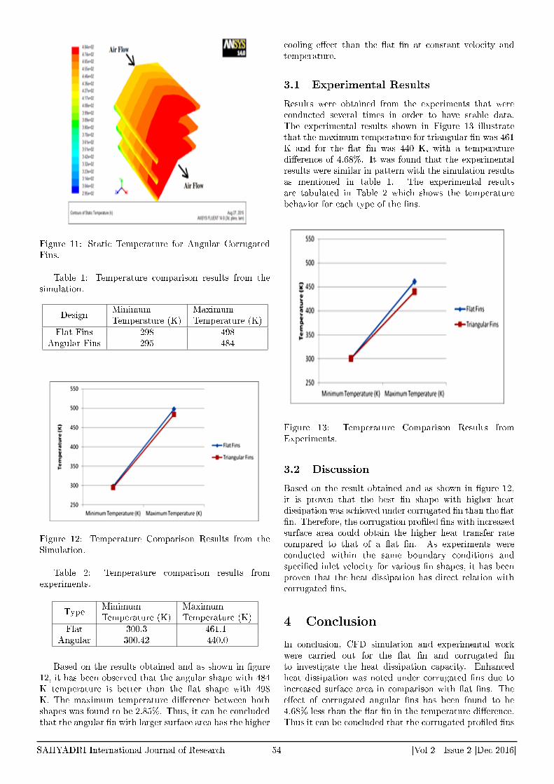
Figure 11: Static Temperature for Angular CorrugatedFins.
Table 1: Temperature comparison results from thesimulation.
DesignMinimumTemperature (K)
MaximumTemperature (K)
Flat Fins 298 498Angular Fins 295 484
Figure 12: Temperature Comparison Results from theSimulation.
Table 2: Temperature comparison results fromexperiments.
TypeMinimumTemperature (K)
MaximumTemperature (K)
Flat 300.3 461.1Angular 300.42 440.0
Based on the results obtained and as shown in �gure12, it has been observed that the angular shape with 484K temperature is better than the �at shape with 498K. The maximum temperature di�erence between bothshapes was found to be 2.85%. Thus, it can be concludedthat the angular �n with larger surface area has the higher
cooling e�ect than the �at �n at constant velocity andtemperature.
3.1 Experimental Results
Results were obtained from the experiments that wereconducted several times in order to have stable data.The experimental results shown in Figure 13 illustratethat the maximum temperature for triangular �n was 461K and for the �at �n was 440 K, with a temperaturedi�erence of 4.68%. It was found that the experimentalresults were similar in pattern with the simulation resultsas mentioned in table 1. The experimental resultsare tabulated in Table 2 which shows the temperaturebehavior for each type of the �ns.
Figure 13: Temperature Comparison Results fromExperiments.
3.2 Discussion
Based on the result obtained and as shown in �gure 12,it is proven that the best �n shape with higher heatdissipation was achieved under corrugated �n than the �at�n. Therefore, the corrugation pro�led �ns with increasedsurface area could obtain the higher heat transfer ratecompared to that of a �at �n. As experiments wereconducted within the same boundary conditions andspeci�ed inlet velocity for various �n shapes, it has beenproven that the heat dissipation has direct relation withcorrugated �ns.
4 Conclusion
In conclusion, CFD simulation and experimental workwere carried out for the �at �n and corrugated �nto investigate the heat dissipation capacity. Enhancedheat dissipation was noted under corrugated �ns due toincreased surface area in comparison with �at �ns. Thee�ect of corrugated angular �ns has been found to be4.68% less than the �at �n in the temperature di�erence.Thus it can be concluded that the corrugated pro�led �ns
SAHYADRI International Journal of Research 54 |Vol 2| Issue 2 |Dec 2016|

have an improved heat dissipation and would be e�cientin heat transfer applications.
References
[1] P. K. Kasana, "Computation of Heat TransferAugmentation in a plate-�n heat Exchanger usingRectangular/Delta Wing", KURUKSHETRA-136119,India, 2010.
[2] Y. A. Cengel, "Heat and Mass Transfer: (SI Units):A Practical Approach", 3rd edition, 2006.
[3] G. Jogi Nikhil and M. Lawankar Shailendra, "Heattransfer analysis of corrugated plate heat exchangerof di�erent plate geometry: A review", IJETAE, vol.2, pp. 110-115, 2012.
[4] Tisekar Salman, A. Mukadam Shakeb, VedapathakHarshad S, Rasal Priyanka K and Khandekar S.B,"Performance analysis of corrugated plate heatexchanger with water as working �uid", IJRET, vol.5, pp. 56-62, 2016.
[5] Khoshvaght Aliabadi, Khoshvaght and Rahnama,"Thermal hydraulic characteristics of plate �n heatexchangers with corrugated/vortex-generator plate �n
(CVGPF)", Applied Thermal Engineering, vol. 98, pp.690-701, 2016.
[6] Zhao Gang Qi, Jiang Ping Chen and Zhi Jiu Chen,"Parametric study on the performance of a heatexchanger with corrugated louvered �ns", AppliedThermal Engineering, Vol. 27, pp. 539-544, 2006.
[7] Kijung Ryu and Kwan Soo Lee, "Generalized heattransfer and �uid �ow correlations for corrugatedlouvered �ns", Int. J. of heat and mass transfer, Vol.83, pp. 604-612, 2015.
[8] Kijung Ryu and Kwan Soo Lee, "Optimal designof a corrugated louvered �n", Applied thermalengineering, vol. 68, pp.76-79, 2014.
[9] Jang Won Seo, Chanyong Cho, Sangrae Lee andYoung Don Choi, "Thermal characteristics of aprimary surface heat exchanger with corrugatedchannels", Entropy, vol. 18, pp. 1-16, 2015.
[10] D. Kumbhar, N. K. Sane and C. S. T, "FiniteElement Analysis and Experimental Study ofConvective Heat Transfer Augmentation fromHorizontal Rectangular Fin by TriangularPerforations," in Int. Conference on Advances inMechanical Engineering, Gujarat, 2009.
SAHYADRI International Journal of Research 55 |Vol 2| Issue 2 |Dec 2016|
Study of E�ect of Heat Treatment Processes On
Material Properties of Manganese SteelsG. Sandesh Kumar Rai1, Vishwanatha Nayak2, Ravindra Mallya1, J. Rohith Acharya1, P. Rajesh Rai3
1Mechanical Engineering Dept., Canara Engineering College, Bantwal, Mangalore-5742192Mangalore Marine College and Technology Kuppepadavu Post, Mangalore, Karnataka 574144
3AJ Institute of Engineering and Technology, Bangrakuloor, Kodikal, Mangalore, Karnataka 575013
Email:[email protected]
AbstractHeat treatment on manganese steel improves ductility,toughness, hardness and tensile strength and to relieveinternal stress developed in the material. The hardnesstest, impact test, wear test, compression test andmicrostructure analysis were conducted on heat treatedmanganese steel, which has extensive uses in all industriesincluding electronic, research and development �elds.The manganese steel properties can be varied with thevarious heat treatment processes such as annealing,tempering, normalising, hardening and spheroidising.The material is given a micro �nish for performingthe microstructure analysis. The micro �nish of theheat-treated specimen was super-�nished in the singledisc polishing machine. The polished specimens wereetched for �nding the exact microstructure. Theoptical microstructure images were taken at di�erentmagni�cations and were studied.The test results show that tempering can be doneto increase the toughness, annealing can be done toincrease the toughness and ductility, normalising canbe done to improve the hardness with some ductility andspheroidising to increase the machinability.
Keywords:-annealing, charpy test, hardening,normalizing, spheroidising and tempering.
1 Introduction
Steel has many practical applications in every aspect oflife. The manganese steel is very important material forthe industries working on metals including electronics.Manganese is hard and very brittle, di�cult to fuse,but easy to oxidize. Manganese steel having manganesecontent of 1-1.5% makes the steel strong and toughand manganese content from 2-5% makes the steel hardand brittle. When manganese is from 11-14%, steelbecomes very hard, tough, and nonmagnetic and possessesconsiderably high tensile strength. Manganese steel showshigh percentage of elongation. It can be forged easily butdi�cult to be machined. Speci�c gravity of manganesesteel is 7.2, melting point 1343◦C. Compositions ofmanganese steel are: Carbon 1.2-1.6%, Manganese 11-14%, Chromium 1.5-2.5% and Silicon 0.5%.
The manganese content in carbon steels is oftenincreased for the purpose of increasing hardening and
improving strength and toughness. Manganese is asilvery-gray metal resembling iron. Manganese is presentin all steels as a de-oxidizer. When manganese is absent orvery low, the predominant sulphide is iron sulphide (FeS),which forms the eutectic with iron, has a�nity to formthin continuous �lms around the primary crystals duringsolidi�cation of the steel. A higher content of manganesein the presence of carbon substantially increases the wearresistance.
The process of heat treatment is carried out �rst byheating the metal and then cooling it in water, air, oiland brine water. The purpose of heat treatment is tosoften the metal, to change the grain size, to modifythe structure of the material and relieve the stress inthe material. The various heat treatment processesare annealing, normalizing, hardening, tempering andspheroidising.
Heat Treatment is the controlled heating and coolingof metals to alter their physical and mechanical propertieswithout changing the product shape.
The most important heat treatments and theirpurposes are:a) Normalizing - it will improve strength along with someductility;b) Surface hardening - Produces a local wear resistanthard surface by induction, �ame, or laser;c) Hardening and tempering - it will increase hardnessand gives improved strength and higher proof stress ratio;d) Stress relieving - to reduce or relieve Internal stressesremained after casting and a low-temperature heattreatment;e) Austempering - it will yield to give bainitic structuresof high strength along with signi�cant ductility and goodwear resistance;f) Annealing - It will improve ductility and toughness andreduce hardness.
L.A. Dobrzanski et al [1] have investigatedhigh-manganese austenitic steels with Nb and Timicroadditions in variable conditions of hot-working,which showed microstructure evolution in variousconditions of plastic deformation. Microstructure of steelwas subjected to solution heat treatment at temperatureof 900◦C and obtained �ne-grained microstructure ofaustenite phase.
In their subsequent work [2] they have determinedthe force-energetic parameters of hot-working in hot-compression tests carried out in a temperature range
SAHYADRI International Journal of Research 56 |Vol 2| Issue 2 |Dec 2016|

of 850 to 1050◦C. They reported that the dynamicrecrystallization leads to structure re�nement attemperature 850◦C.
J. Adamczyk et al [3] have determined the in�uenceof the initial structure and heat treatment conditionson mechanical properties of DP-type steel. They haverealized DP-type structure of desirable ferrite andmartensite fractions by heat treatment of the low-carbonsteel. Mechanical properties were determined by meansof tensile test. They have reported that heat treatmentconditions can be useful for manufacturing DP-type steelsheets of high strength and ductile properties and a goodsuitability for metalforming operations.
K.D. Clarke et al [4] have studied the inductionhardening heat treatments using dilatometry on 5150steel with ferrite-pearlite and tempered martensite initialmicrostructures to assess e�ects of prior microstructureand heating rate. They opined that transformationtemperatures are signi�cantly higher for a ferrite-pearliteinitial microstructure than for a tempered martensiteprior microstructure. They have found that maximumhardness is independent of starting microstructure, for agiven thermal cycle.
L.A. Dobrzanski et al [5] have determined the in�uenceof hot-working conditions on microstructure evolutionand phase composition of high-manganese austeniticsteels. They found that steels have a �ne-grainedaustenite microstructure with many twins at an annealingtemperature of about 1000◦C. This microstructure of steelcan be useful in determining power-force parameters forhot-rolling of sheets.
2 Experimental
The experimental procedures adopted for this researchwork can be listed as follows:Specimen preparationHeat treatmentHardness measurementImpact testingWear measurementCompression strength measurementMicrostructure study
The specimens were prepared from grade 3 manganesesteel based on required volume of material. Theproperties can be varied with the various heat treatmentprocesses such as annealing, tempering, normalising,hardening and spheroidising which were carried out onmanganese steel by varying the soaking time of each heattreatment to three di�erent timings i.e., 30,45 and 60 min.
The heat-treated materials were then subjected todi�erent material testing processes like hardness test,compression test, wear test and impact test. Vickershardness testing machine is used for �nding the hardness,pin on disc machine for wear test, Charpy impact testingmachine to �nd the impact strength and universal testingmachine (UTM) is used to �nd the compression strength.
The material testing is done for the entire specimenswith di�erent heat treatment processes and also for thespecimens without heat treatment.
Microstructure analysis and metallography are usuallyconducted to determine the material′s response to thermalheat treatment. The sample to be studied is often wetabrasive sectioned, cleaned and mounted in bakelite or aresin to hold it during grinding and polishing.
Later the material is given a micro �nish forperforming the micro structure analysis. The surfaceof the heat treated specimen was super �nished in thesingle disc polishing machine. The polished specimensare etched for �nding the exact micro structure. Themicrostructure was studied at di�erent magni�cations.
3 Results and Discussions
3.1 Test results
The hardness test, compression test, wear test andimpact test were conducted on these manganese steeltest specimens before and after heat treatment processes.The material testing like compression test, impact test,wear test, hardness tests and microstructure analysis wereconducted to �nd the e�ect of heat treatment process onthe specimens. The values were calculated and tabulatedin Table 1.
Table 1: Vickers hardness test speci�cation beforeheat-treatment.
Load (kgf) 30
Diameter (d1) (mm) 0.440
Diameter (d2)(mm) 0.439
Mean diameter (d)(mm) 0.439
Vickers Hardness Number (VHN) 286.42
Figure 1: Variation of VHN with soaking time.
Figure 1 shows hardness of specimens under variousheat treatment processes. Spherodising process makes thematerial softer. Hardening process makes the materialharder with soaking time and all other processes come inbetween.
SAHYADRI International Journal of Research 57 |Vol 2| Issue 2 |Dec 2016|
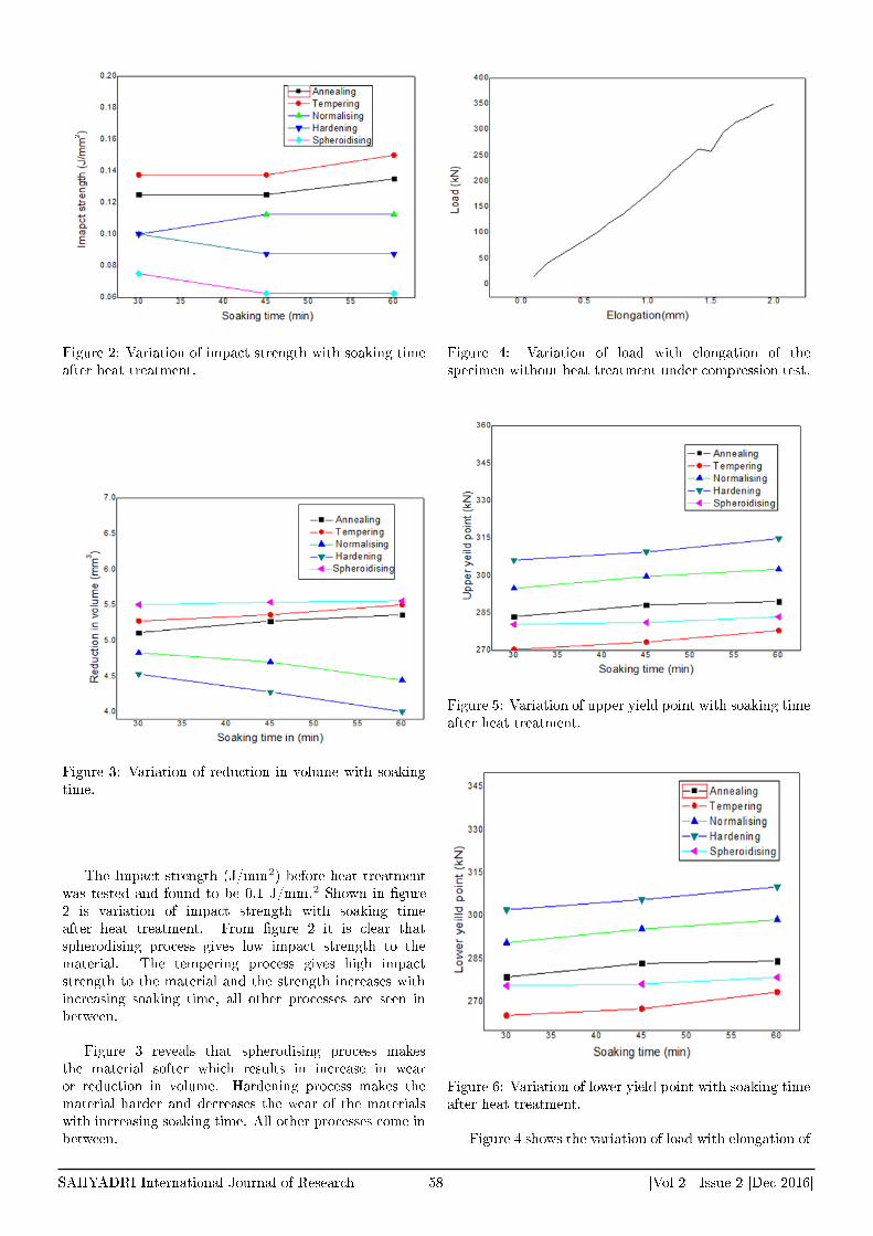
Figure 2: Variation of impact strength with soaking timeafter heat treatment.
Figure 3: Variation of reduction in volume with soakingtime.
The Impact strength (J/mm2) before heat treatmentwas tested and found to be 0.1 J/mm.2 Shown in �gure2 is variation of impact strength with soaking timeafter heat treatment. From �gure 2 it is clear thatspherodising process gives low impact strength to thematerial. The tempering process gives high impactstrength to the material and the strength increases withincreasing soaking time, all other processes are seen inbetween.
Figure 3 reveals that spherodising process makesthe material softer which results in increase in wearor reduction in volume. Hardening process makes thematerial harder and decreases the wear of the materialswith increasing soaking time. All other processes come inbetween.
Figure 4: Variation of load with elongation of thespecimen without heat treatment under compression test.
Figure 5: Variation of upper yield point with soaking timeafter heat treatment.
Figure 6: Variation of lower yield point with soaking timeafter heat treatment.
Figure 4 shows the variation of load with elongation of
SAHYADRI International Journal of Research 58 |Vol 2| Issue 2 |Dec 2016|

the specimen without heat-treatment under compressiontest. It is seen from the �gure that upper yield pointis 262.24 kN and lower yield point is 257.64 kN. Figure5 shows the upper yield point in a compression testof specimens under various heat treatment processes.Tempering process decreases the compression strengthof the material. Hardening process increases thecompression strength of the material with increasingsoaking time. Figure 6 shows lower yield point ina compression test of specimens under various heattreatment processes. Tempering process decreases thecompression strength of the material. Hardening processincreases the compression strength of the material withincreasing soaking time. All other process come inbetween.
3.2 Microstructure Analysis
Figure 7 shows Optical microstructure of manganese steelbefore and after heat-treatment for 30,45 and 60 min. α-ferrite and pearlite phases, are seen; the pearlite structureis distributed in α-ferrite.
Figure 7: Optical microstructure of manganese steel:(a) without heat treatment;(b) after annealing with 30min. soaking time;(c) after annealing with 45min. soaking time;(d) after annealing with 60min. soaking time.
In �gure 7 (d) the α-ferrite and pearlite phases areevenly distributed and are denser than that for 30 and 45minutes of soaking. The property of the pearlite phaseis to improve the toughness of the steel and reduce thehardness which is seen in microstructure after annealingwith 60min. soaking time.
In �gure 8 the α-ferrite and pearlite matrix is seenclearly. The property of the pearlite is to improve thetoughness and α-ferrite is to improve the mechanicalproperty. Thus, tempering reduces the hardness andimproves toughness of the materials which is seen after
tempering with 60 minutes of soaking time. Thetoughness increased when compared with 30 minutes ofsoaking time.
Figure 8: Optical microstructure of manganese steel:(a)after tempering with 30min. soaking time;(b)after tempering with 60min. soaking time.
Figure 9: Optical microstructure of manganese steel:(a) after hardening with 30min. soaking time;(b) after hardening with 60min. soaking time.
The α-ferrite and pearlite in martensite matrix is seenin �gure 9(a). The property of the martensite is toimprove the hardness of the material. The hardness of thematerial is due to the presence of martensite as seen inmicrostructure after hardening with 30 minutes of soakingtime. The Martensite reduces the toughness.
Figure 9(b) shows the presence of α-ferrite and pearlitein martensite matrix. The martensite found in �gure 9(a)is denser than the martensite seen in hardening with 60minutes soaking time. The property of the martensite isto improve the hardness. And it is seen in the �gure thatsoaking increases the hardness of the material and theincrease in hardness is due to the presence of martensitephase.
SAHYADRI International Journal of Research 59 |Vol 2| Issue 2 |Dec 2016|
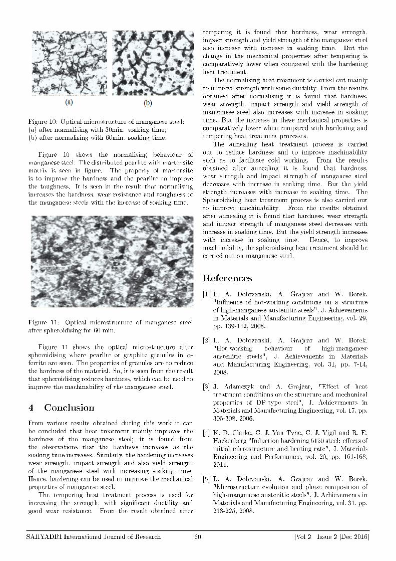
Figure 10: Optical microstructure of manganese steel:(a) after normalising with 30min. soaking time;(b) after normalising with 60min. soaking time.
Figure 10 shows the normalising behaviour ofmanganese steel. The distributed pearlite with martensitematrix is seen in �gure. The property of martensiteis to improve the hardness and the pearlite to improvethe toughness. It is seen in the result that normalisingincreases the hardness, wear resistance and toughness ofthe manganese steels with the increase of soaking time.
Figure 11: Optical microstructure of manganese steelafter spheroidising for 60 min.
Figure 11 shows the optical microstructure afterspheroidising where pearlite or graphite granules in α-ferrite are seen. The properties of granules are to reducethe hardness of the material. So, it is seen from the resultthat spheroidising reduces hardness, which can be used toimprove the machinability of the manganese steel.
4 Conclusion
From various results obtained during this work it canbe concluded that heat treatment mainly improves thehardness of the manganese steel; it is found fromthe observations that the hardness increases as thesoaking time increases. Similarly, the hardening increaseswear strength, impact strength and also yield strengthof the manganese steel with increasing soaking time.Hence, hardening can be used to improve the mechanicalproperties of manganese steel.
The tempering heat treatment process is used forincreasing the strength, with signi�cant ductility andgood wear resistance. From the result obtained after
tempering it is found that hardness, wear strength,impact strength and yield strength of the manganese steelalso increase with increase in soaking time. But thechange in the mechanical properties after tempering iscomparatively lower when compared with the hardeningheat treatment.
The normalising heat treatment is carried out mainlyto improve strength with some ductility. From the resultsobtained after normalising it is found that hardness,wear strength, impact strength and yield strength ofmanganese steel also increases with increase in soakingtime. But the increase in these mechanical properties iscomparatively lower when compared with hardening andtempering heat treatment processes.
The annealing heat treatment process is carriedout to reduce hardness and to improve machinabilitysuch as to facilitate cold working. From the resultsobtained after annealing it is found that hardness,wear strength and impact strength of manganese steeldecreases with increase in soaking time. But the yieldstrength increases with increase in soaking time. TheSpheroidising heat treatment process is also carried outto improve machinability. From the results obtainedafter annealing it is found that hardness, wear strengthand impact strength of manganese steel decreases withincrease in soaking time. But the yield strength increaseswith increase in soaking time. Hence, to improvemachinability, the spheroidising heat treatment should becarried out on manganese steel.
References
[1] L. A. Dobrzanski, A. Grajcar and W. Borek,"In�uence of hot-working conditions on a structureof high-manganese austenitic steels", J. Achievementsin Materials and Manufacturing Engineering, vol. 29,pp. 139-142, 2008.
[2] L. A. Dobrzanski, A. Grajcar and W. Borek,"Hot-working behaviour of high-manganeseaustenitic steels", J. Achievements in Materialsand Manufacturing Engineering, vol. 31, pp. 7-14,2008.
[3] J. Adamczyk and A. Grajcar, "E�ect of heattreatment conditions on the structure and mechanicalproperties of DP-type steel", J. Achievements inMaterials and Manufacturing Engineering, vol. 17, pp.305-308, 2006.
[4] K. D. Clarke, C. J. Van Tyne, C. J. Vigil and R. E.Hackenberg "Induction hardening 5150 steel: e�ects ofinitial microstructure and heating rate", J. MaterialsEngineering and Performance, vol. 20, pp. 161-168,2011.
[5] L. A. Dobrzanski, A. Grajcar and W. Borek,"Microstructure evolution and phase composition ofhigh-manganese austenitic steels", J. Achievements inMaterials and Manufacturing Engineering, vol. 31, pp.218-225, 2008.
SAHYADRI International Journal of Research 60 |Vol 2| Issue 2 |Dec 2016|
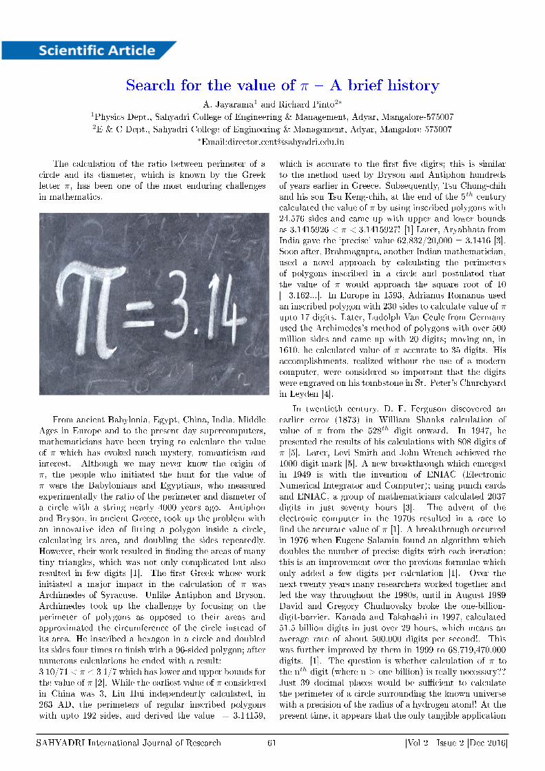
Search for the value of π � A brief historyA. Jayarama1 and Richard Pinto2∗
1Physics Dept., Sahyadri College of Engineering & Management, Adyar, Mangalore-5750072E & C Dept., Sahyadri College of Engineering & Management, Adyar, Mangalore-575007
∗Email:[email protected]
The calculation of the ratio between perimeter of acircle and its diameter, which is known by the Greekletter π, has been one of the most enduring challengesin mathematics.
From ancient Babylonia, Egypt, China, India, MiddleAges in Europe and to the present day supercomputers,mathematicians have been trying to calculate the valueof π which has evoked much mystery, romanticism andinterest. Although we may never know the origin ofπ, the people who initiated the hunt for the value ofπ were the Babylonians and Egyptians, who measuredexperimentally the ratio of the perimeter and diameter ofa circle with a string nearly 4000 years ago. Antiphonand Bryson, in ancient Greece, took up the problem withan innovative idea of �tting a polygon inside a circle,calculating its area, and doubling the sides repeatedly.However, their work resulted in �nding the areas of manytiny triangles, which was not only complicated but alsoresulted in few digits [1]. The �rst Greek whose workinitiated a major impact in the calculation of π wasArchimedes of Syracuse. Unlike Antiphon and Bryson,Archimedes took up the challenge by focusing on theperimeter of polygons as opposed to their areas andapproximated the circumference of the circle instead ofits area. He inscribed a hexagon in a circle and doubledits sides four times to �nish with a 96-sided polygon; afternumerous calculations he ended with a result:3 10/71 < π < 3 1/7 which has lower and upper bounds forthe value of π [2]. While the earliest value of π consideredin China was 3, Liu Hui independently calculated, in263 AD, the perimeters of regular inscribed polygonswith upto 192 sides, and derived the value = 3.14159,
which is accurate to the �rst �ve digits; this is similarto the method used by Bryson and Antiphon hundredsof years earlier in Greece. Subsequently, Tsu Chung-chihand his son Tsu Keng-chih, at the end of the 5th centurycalculated the value of π by using inscribed polygons with24,576 sides and came up with upper and lower boundsas 3.1415926 < π < 3.1415927! [1] Later, Aryabhata fromIndia gave the 'precise' value 62,832/20,000 = 3.1416 [3].Soon after, Brahmagupta, another Indian mathematician,used a novel approach by calculating the perimetersof polygons inscribed in a circle and postulated thatthe value of π would approach the square root of 10[=3.162...]. In Europe in 1593, Adrianus Romanus usedan inscribed polygon with 230 sides to calculate value of πupto 17 digits. Later, Ludolph Van Ceule from Germanyused the Archimedes's method of polygons with over 500million sides and came up with 20 digits; moving on, in1610, he calculated value of π accurate to 35 digits. Hisaccomplishments, realized without the use of a moderncomputer, were considered so important that the digitswere engraved on his tombstone in St. Peter's Churchyardin Leyden [4].
In twentieth century, D. F. Ferguson discovered anearlier error (1873) in William Shanks calculation ofvalue of π from the 528th digit onward. In 1947, hepresented the results of his calculations with 808 digits ofπ [5]. Later, Levi Smith and John Wrench achieved the1000-digit-mark [5]. A new breakthrough which emergedin 1949 is with the invention of ENIAC (ElectronicNumerical Integrator and Computer); using punch cardsand ENIAC, a group of mathematicians calculated 2037digits in just seventy hours [3]. The advent of theelectronic computer in the 1970s resulted in a race to�nd the accurate value of π [1]. A breakthrough occurredin 1976 when Eugene Salamin found an algorithm whichdoubles the number of precise digits with each iteration;this is an improvement over the previous formulae whichonly added a few digits per calculation [1]. Over thenext twenty years many researchers worked together andled the way throughout the 1980s, until in August 1989David and Gregory Chudnovsky broke the one-billion-digit-barrier. Kanada and Takahashi in 1997, calculated51.5 billion digits in just over 29 hours, which means anaverage rate of about 500,000 digits per second!. Thiswas further improved by them in 1999 to 68,719,470,000digits. [1]. The question is whether calculation of π tothe nth digit (where n > one billion) is really necessary??Just 39 decimal places would be su�cient to calculatethe perimeter of a circle surrounding the known universewith a precision of the radius of a hydrogen atom!! At thepresent time, it appears that the only tangible application
SAHYADRI International Journal of Research 61 |Vol 2| Issue 2 |Dec 2016|

of all those digits is to �nd the bugs in computer chipsand computers. Further, mathematicians are also lookingfor the occurrence of some rules that will distinguish thedigits of π from other numbers. But, Chudnovskys havealso opined that no other calculated number comes closeto a random sequence of digits other than that of magicalnumber π.
References
[1] David Blatner, "The Joy of Pi", Walker PublishingCo., Inc., New York, 1997.
[2] https://www.math.rutgers.edu/ cherlin/History/Papers2000/wilson.html.
[3] Petr. Beckman, "The History of Pi", The GolemPress. Boulder, Colorado, 1971.
[4] Florian Cajori, "A History of Mathematics",MacMillan and Co., London, 1926.
[5] Lennart Berggren, Jonathan Borwein and PeterBorwein, "Pi: A Source Book", Springer-Verlag. NewYork, 1997.
SAHYADRI International Journal of Research 62 |Vol 2| Issue 2 |Dec 2016|

Guidelines for Submission
• Authors are requested to provide full details for correspondence: postal
address, phone numbers and email address. (The email address of
corresponding authors will be published along with the article).
• Authors are requested to prepare their soft copy version in text formats and
not in PDF version.
• Authors are requested to follow the manuscript template while preparing the
manuscript.
SIJR is devoted to the publication of original research work. The journal also
accepts review papers and scientific articles. SIJR welcomes the submission of
manuscripts that meet the journal standard which includes novelty, significance
and excellence. Every volume of the journal will have two issue in a year. All
articles published in the SIJR are peer-reviewed.
Contact for any query or Information on
SAHYADRI International Journal of Research
Dr. Richard Pinto - Editor-in-Chief
or
Dr. Jayarama A - Editor
Email: [email protected]
Web: www.sijr.in
Sahyadri Journal of ResearchInternational
64SAHYADRI International Journal of Research
PublisherManjunath Bhandary - President
Bhandary Foundation, Sahyadri Campus, Adyar, Mangaluru - 575 007
PrintersPrakash Offset Printers, 164, Industrial Area, Baikampady, Mangaluru - 575 011
| Vol 2 | Issue 2 | Dec 2016

Sahyadri Campus, Adyar, Mangaluru - 575 007
COLLEGE OF ENGINEERING & MANAGEMENTSAHYADRI
(Affiliated to VTU, Belagavi and Approved by AICTE, New Delhi)
TM
Empowering young minds
+ 91-824-2277222 | + 91 96119 45201 | [email protected] | www.sijr.in | www.sahyadri.edu.inSAHYADRI Journal of Research | December 2015 | 3
Sahyadri campus - The sprawling campus just off the Mangalore-Bangalore National
Highway 48 is situated on the banks of the river Nethravathi. Surrounded with natures pristine
beauty and an excellent infrastructure coupled with dedicated and experienced faculty has made the
Campus a much sought-after abode of learning.