( Top View ) (Top View) 3. GND - diodes.com · stabilized architecture the AH180 provides a...
12
AH180 Document number: DS31023 Rev. 18 - 3 1 of 12 www.diodes.com July 2018 © Diodes Incorporated AH180 MICROPOWER OMNIPOLOAR HALL-EFFECT SENSOR SWITCH Description AH180 is a micro-power Omnipolar Hall-Effect switch designed for portable and battery powered equipment such cellular phones, PDAs and portable PCs. Based on two Hall-Effect plates and a chopper stabilized architecture the AH180 provides a reliable solution over the whole operating range. To support portable and battery powered equipment the design has been optimized to operate over the supply range of 2.5V to 5.5V and consumes only 24uW with a supply of 3V. The single open-drain output switches on with either a north or south pole of sufficient strength. When the magnetic flux density (B) is larger than operate point (Bop), output is switched on (Output pin is pulled low). The output is turned off when B becomes lower than the release point (Brp). The output will remain off when there is no magnetic field. The AH180 is available in SIP-3L, SC59, DFN2020-3, and DFN2020- 6 packages. Features • Omnipolar (north or south pole) operation • Micropower operation • Single open drain output • 2.5V to 5.5V operating voltage • Chopper stabilized design provides • Superior temperature stability • Minimal switch-point drift • Enhanced immunity to stress • Good RF noise immunity • -40°C to +85°C operating temperature • ESD (HBM) > 5KV for DFN2020-6, DFN2020-3 > 6KV for SIP-3L and SC59 • SIP-3L, SC59 (commonly known as SOT23 in Asia) DFN2020-6, DFN2020-3 packages • Green Molding Compound (No Br, Sb) (Note 1) Pin Assignments (Top View) 1. Vdd 2. GND 3. Output (SIP-3L) 1 . Vdd 3. GND 2. Output (Top View) SC59 1. Vdd 2. NC 3. Output 4. NC 6. NC 5. GND (Top View) DFN2020-6 1. Vdd 3. Output 3. GND ( Top View ) DFN2020-3 Applications • Cover Switch in Clam-Shell Cellular Phones • Cover Switch in Notebook PC/PDA • Contactless Switch in Consumer Products Notes: 1. EU Directive 2002/95/EC (RoHS) & 2011/65/EU (RoHS 2) compliant. All applicable RoHS exemptions applied. NOT RECOMMENDED FOR NEW DESIGN USE AH1808
Transcript of ( Top View ) (Top View) 3. GND - diodes.com · stabilized architecture the AH180 provides a...

AH180 Document number: DS31023 Rev. 18 - 3
1 of 12 www.diodes.com
July 2018 © Diodes Incorporated
AH180
MICROPOWER OMNIPOLOAR HALL-EFFECT SENSOR SWITCH
Description
AH180 is a micro-power Omnipolar Hall-Effect switch designed for
portable and battery powered equipment such cellular phones, PDAs
and portable PCs. Based on two Hall-Effect plates and a chopper
stabilized architecture the AH180 provides a reliable solution over the
whole operating range. To support portable and battery powered
equipment the design has been optimized to operate over the supply
range of 2.5V to 5.5V and consumes only 24uW with a supply of 3V.
The single open-drain output switches on with either a north or south
pole of sufficient strength.
When the magnetic flux density (B) is larger than operate point
(Bop), output is switched on (Output pin is pulled low). The output is
turned off when B becomes lower than the release point (Brp). The
output will remain off when there is no magnetic field.
The AH180 is available in SIP-3L, SC59, DFN2020-3, and DFN2020-
6 packages.
Features
• Omnipolar (north or south pole) operation
• Micropower operation
• Single open drain output
• 2.5V to 5.5V operating voltage
• Chopper stabilized design provides
• Superior temperature stability
• Minimal switch-point drift
• Enhanced immunity to stress
• Good RF noise immunity
• -40°C to +85°C operating temperature
• ESD (HBM) > 5KV for DFN2020-6, DFN2020-3
> 6KV for SIP-3L and SC59
• SIP-3L, SC59 (commonly known as SOT23 in Asia) DFN2020-6,
DFN2020-3 packages
• Green Molding Compound (No Br, Sb) (Note 1)
Pin Assignments
(Top View)
1. Vdd
2. GND
3. Output
(SIP-3L)
1 . Vdd
3.
GND 2.
Output
(Top View)
SC59
1. Vdd 2. NC 3. Output
4. NC6. NC 5. GND
(Top View)
DFN2020-6 1. Vdd 3. Output
3. GND
( Top View )
DFN2020-3
Applications
• Cover Switch in Clam-Shell Cellular Phones
• Cover Switch in Notebook PC/PDA
• Contactless Switch in Consumer Products
Notes: 1. EU Directive 2002/95/EC (RoHS) & 2011/65/EU (RoHS 2) compliant. All applicable RoHS exemptions applied.
NOT RECOMMENDED FOR NEW DESIGN USE AH1808
AH180 Document number: DS31023 Rev. 18 - 3
2 of 12 www.diodes.com
July 2018 © Diodes Incorporated
AH180
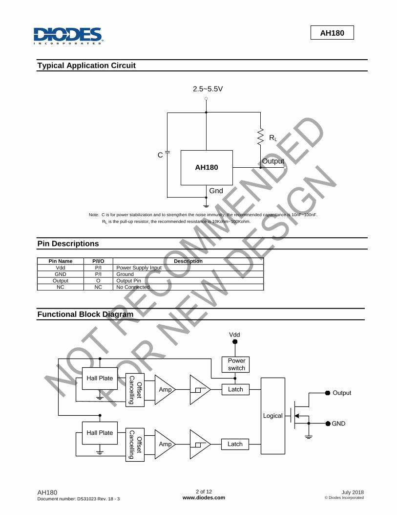
Typical Application Circuit
AH180
2.5~5.5V
Output
Gnd
RL
C
Note: C is for power stabilization and to strengthen the noise immunity, the recommended capacitance is 10nF~100nF.
RL is the pull-up resistor, the recommended resistance is 10Kohm~100Kohm.
Pin Descriptions
Functional Block Diagram
Output
GND
Logical
Latch
Latch
Power
switch
Vdd
Hall Plate
Amp
Offs
et
Ca
nce
lling
Hall Plate
Amp
Offs
et
Ca
nce
lling
Pin Name P/I/O Description
Vdd P/I Power Supply Input
GND P/I Ground
Output O Output Pin
NC NC No Connected

AH180 Document number: DS31023 Rev. 18 - 3
3 of 12 www.diodes.com
July 2018 © Diodes Incorporated
AH180
Absolute Maximum Ratings (TA = +25°C)
Symbol Characteristics Values Unit
Vdd Supply voltage 7 V
B Magnetic flux density Unlimited
Ts Storage Temperature Range -65 to +150 C
PD Package Power Dissipation
SIP-3L 550 mW
SC59-3L/ DFN2020-6/ DFN2020-3
230 mW
TJ Maximum Junction Temperature 150 C
Recommended Operating Conditions
Symbol Parameter Conditions Min Max Unit
Vdd Supply Voltage Operating 2.5 5.5 V
TA Operating Ambient Temperature Operating -40 85 C
Electrical Characteristics (TA = +25°C, Vdd = 3V; unless otherwise specified)
Symbol Characteristic Conditions Min Typ. Max Unit
Vout Output On Voltage Iout =1mA 0.1 0.3 V
Ioff Output Leakage Current Vout =5.5V, Output off <0.1 1 µA
Idd(en)
Supply Current
Chip enable, TA = +25°C, Vdd = 3V 3 6 mA
Idd(en) Chip enable, TA = -40~85°C,
Vdd = 2.5~5.5V 3 9 mA
Idd(dis) Chip disable, TA = +25°C, Vdd = 3V 5 10 µA
Idd(dis) Chip disable, TA = -40~85C,
Vdd = 2.5~5.5V 5 15 µA
Idd(avg) Average supply current,
TA = +25°C, Vdd = 3V 8 16 µA
Idd(avg) Average supply current,
TA = -40~85C, Vdd = 2.5~5.5V 8 24 µA
Tawake Awake Time (Note 2) 75 125 µs
Tperiod Period (Note 2) 75 125 ms
D.C. Duty Cycle 0.1 %
Note: 2. When power is initially turned on, Vdd must be within its correct operating range (2.5V to 5.5V) to guarantee the output sampling. The output state is valid after the second operating phase (typical 150ms).
Idd (dis)
Idd(en)
Tawake
Tperiod
0
Sample and output
latched

AH180 Document number: DS31023 Rev. 18 - 3
4 of 12 www.diodes.com
July 2018 © Diodes Incorporated
AH180
Magnetic Characteristics (TA = +25°C, Vdd = 3V, Notes 3 & 4)
Option 1: (1mT=10 Gauss)
Symbol Parameter Min Typ. Max Unit
Bops (south pole to brand side) Operation Point
- 40 60
Gauss
Bopn (north pole to brand side) -60 -40 -
Brps (south pole to brand side) Release Point
10 30 -
Brpn (north pole to brand side) - -30 -10
Bhy (|Bopx|-|Brpx|) Hysteresis - 15 -
Option 2: (1mT=10 Gauss)
Symbol Parameter Min Typ. Max Unit
Bops (south pole to brand side) Operation Point
- 40 60
Gauss
Bopn (north pole to brand side) -60 -40 -
Brps (south pole to brand side) Release Point
20 30 -
Brpn (north pole to brand side) - -30 -20
Bhy (|Bopx|-|Brpx|) Hysteresis - 15 -
Notes: 3. Typical data is at TA = +25C, Vdd = 3V, and for design information only. 4. Magnetic characteristics may vary with supply voltage, operating temperature and after soldering.
Operating Characteristics
Bhy
Vsat
Vcc
( O
utp
ut
Vo
lta
ge
)
Bopn Brpn 0( Magnetic flux density B )
Output
Turn on
Turn off
( off-state )
( on-state )
Bhy
Vsat
Vcc
( O
utp
ut
Vo
lta
ge
)
Brps Bops0( Magnetic flux density B )
Output
Turn offTurn on
( off-state )
( on-state )

AH180 Document number: DS31023 Rev. 18 - 3
5 of 12 www.diodes.com
July 2018 © Diodes Incorporated
AH180
Performance Characteristics
(1) SIP-3L
TA (C) 25 50 60 70 80 85 90 95 100
PD (mW) 550 440 396 352 308 286 264 242 220
TA (C) 105 110 115 120 125 130 135 140 150
PD (mW) 198 176 154 132 110 88 66 44 0
Power Dissipation Curve
0
100
200
300
400
500
600
0 25 50 75 100 125 150TA (
oC)
PD (mW)
85-40
(2) SC59 (commonly known as SOT23 in Asia), DFN2020-6 and DFN2020-3
TA (C) 25 50 60 70 80 85 90 100 110 120 130 140 150
PD (mW) 230 184 166 147 129 120 110 92 74 55 37 18 0
Power Dissipation Curve
0
100
200
300
0 25 50 75 100 125 150
TA (oC)
PD (mW)
85-40

AH180 Document number: DS31023 Rev. 18 - 3
6 of 12 www.diodes.com
July 2018 © Diodes Incorporated
AH180
Ordering Information
AH 180 - XX X - X X
Packing
P : SIP-3L
Lead Free
W : SC59SN : DFN2020-6
A : Ammo Box (Note 9)
7 : Tape & Reel
G : Green (Note 5, 6)B : Bulk (Note 10)
Package
FJ : DFN2020-3
Magnetic Characteristics
(Note 11)
-S : Option 2Blank : Option 1
Device
Status (Note )
Package Code
Packaging (Notes 7 & 8)
Bulk 7” Tape and Reel Ammo Box Magentic
Characteristics (Note 11)
Quantity Part
Number Suffix
Quantity Part
Number Suffix
Quantity Part
Number Suffix
AH180-PG-B NRND P SIP-3L 1000 -B NA NA NA NA Blank
AH180-PG-A NRND P SIP-3L NA NA NA NA -A 4000/Box Blank
AH180-PG-B-S NRND P SIP-3L 1000 -B NA NA NA NA S
AH180-PG-A-S NRND P SIP-3L NA NA NA NA -A 4000/Box S
AH180-WG-7 NRND W SC59 NA NA 3000/Tape & Reel -7 NA NA Blank
AH180-SNG-7 NRND SN DFN2020-6 NA NA 3000/Tape & Reel -7 NA NA Blank
AH180-FJG-7 NRND FJ DFN2020-3 NA NA 3000/Tape & Reel -7 NA NA Blank
Notes: 5. SIP-3L,SC59, DFN2020-6 and DFN2020-3 are available in “Green” 6. EU Directive 2002/95/EC (RoHS). All applicable RoHS exemptions applied. Please visit our website at http://www.diodes.com/products/lead_free.html.
7. Pad layout as shown on Diodes Inc. suggested pad layout document AP02001, which can be found on our website at http://www.diodes.com/datasheets/ap02001.pdf. 8. Reverse taping as shown on Diodes Inc. Surface Mount (SMD) Packaging document AP02007, which can be found on our website http://www.diodes.com/datasheets/ap02007.pdf.
9. Ammo Box is for SIP-3L Spread Lead. 10. Bulk is for SIP-3L Straight Lead.
11. Please refer the Magnetic Characteristics table, option 2 is available in SIP-3L package only. 12 NRND = Not Recommended for New Design
Marking Information
(1) SIP-3L
180Part Number
(Top View)
X : Internal Code : A~Z : Green
Y : Year : 0~9WW : Week : 01~52, "52" represents
52 and 53 weekY WW X
a~z : Lead Free

AH180 Document number: DS31023 Rev. 18 - 3
7 of 12 www.diodes.com
July 2018 © Diodes Incorporated
AH180
Marking Information (cont.)
(2) SC59 (commonly known as SOT23 in Asia)
XX Y W X
( Top View )
XX : Identification code
W : Week : A~Z : 1~26 week;
X : A~Z : Green
Y : Year 0~9
a~z : 27~52 week; z represents52 and 53 week
Part Number Package Identification Code
AH180 SC59 K0
(3) DFN2020-6
( Top View )
180
Pin 1 indicator
Y : Year : 0~9
X : A~Z : Green
W : Week : A~Z : 1~26 week; a~z : 27~52 week; z represents52 and 53 week
Y WX
(4) DFN2020-3
( Top View )
X X
Pin 1 indicator
Y : Year : 0~9
X : A~Z : Green
XX : Identification Code
W : Week : A~Z : 1~26 week; a~z : 27~52 week; z represents52 and 53 week
Y WX
Part Number Package Identification Code
AH180 DFN2020-3 K0
AH180 Document number: DS31023 Rev. 18 - 3
8 of 12 www.diodes.com
July 2018 © Diodes Incorporated
AH180
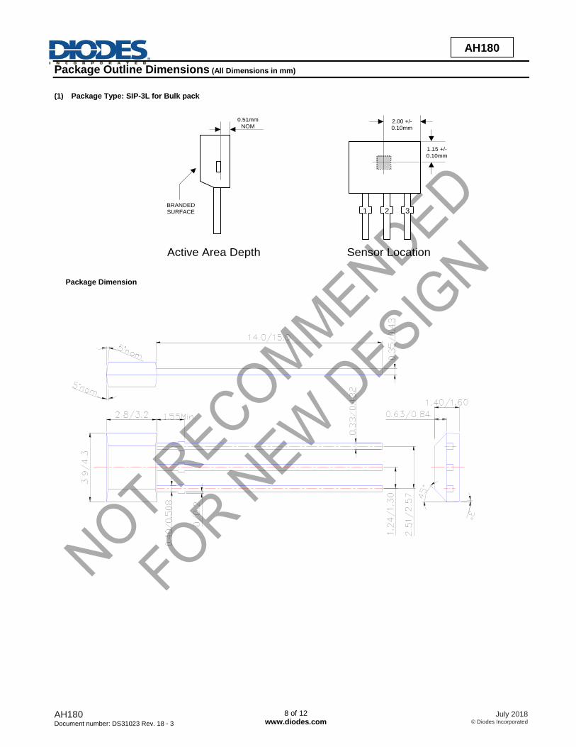
Package Outline Dimensions (All Dimensions in mm)
(1) Package Type: SIP-3L for Bulk pack
Active Area Depth Sensor Location
1 2 3
2.00 +/-
0.10mm
1.15 +/-
0.10mm
0.51mm
NOM
BRANDED
SURFACE
Package Dimension
AH180 Document number: DS31023 Rev. 18 - 3
9 of 12 www.diodes.com
July 2018 © Diodes Incorporated
AH180
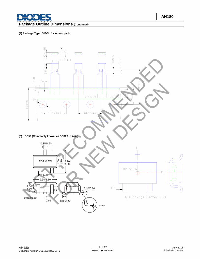
Package Outline Dimensions (Continued)
(2) Package Type: SIP-3L for Ammo pack
(3) SC59 (Commonly known as SOT23 in Asia)
0.35/0.50
0.10/0.20
0.013/0.10
0.35/0.550.95
2.70/3.00
2.90/3.10
1.00/1.30
1.5
0/
1.7
0
1.90
TOP VIEW
0O /8O

AH180 Document number: DS31023 Rev. 18 - 3
10 of 12 www.diodes.com
July 2018 © Diodes Incorporated
AH180
Package Outline Dimensions (Continued)
(4) Package Type: DFN2020-6
0.05 M C A B
B
0.1
5
Bottom View
A
C
0/0
.05
0.5
7/0
.63
0.1
5m
ax.
C
0.15 C2x-
2x
0.08 C
0.05 C
Seating plane
1.45/1.65
1.95/2.075
0.3
0/0
.40
0.2/0.30.65nom.
0.7
6/0
.96
1.9
5/2
.07
5Pin#1 ID
R0.1
Sensor location
Marking 0.4
3m
on
.
(Active area depth)
(5) Package Type: DFN2020-3
0.8
/1.0
1.9
5/2
.075
R0.2
1.1/1.3 0.325(Ref.)
B
0.25 B2x-
0.10M C A B0.2/0.3
0.5Typ
0.3
5/0
.45
0.1
38(R
ef.
)
0/0
.05
0.5
7/0
.63
Typ 0
.60
0.10 C
0.08 C
1.95/2.075A
0.2
5A
2x
C
Seating plane
0.1
3M
ax.
Bottom View
Sensor location
CL
CL

AH180 Document number: DS31023 Rev. 18 - 3
11 of 12 www.diodes.com
July 2018 © Diodes Incorporated
AH180
Taping Orientation (Note 12)
(1) DFN2020-6
(2) DFN2020-3
Note: 12. The taping orientation of the other package type can be found on our website at http://www.diodes.com/datasheets/ap02007.pdf.

AH180 Document number: DS31023 Rev. 18 - 3
12 of 12 www.diodes.com
July 2018 © Diodes Incorporated
AH180
IMPORTANT NOTICE DIODES INCORPORATED MAKES NO WARRANTY OF ANY KIND, EXPRESS OR IMPLIED, WITH REGARDS TO THIS DOCUMENT, INCLUDING, BUT NOT LIMITED TO, THE IMPLIED WARRANTIES OF MERCHANTABILITY AND FITNESS FOR A PARTICULAR PURPOSE (AND THEIR EQUIVALENTS UNDER THE LAWS OF ANY JURISDICTION). Diodes Incorporated and its subsidiaries reserve the right to make modifications, enhancements, improvements, corrections or other changes without further notice to this document and any product described herein. Diodes Incorporated does not assume any liability arising out of the application or use of this document or any product described herein; neither does Diodes Incorporated convey any license under its patent or trademark rights, nor the rights of others. Any Customer or user of this document or products described herein in such applications shall assume all risks of such use and will agree to hold Diodes Incorporated and all the companies whose products are represented on Diodes Incorporated website, harmless against all damages. Diodes Incorporated does not warrant or accept any liability whatsoever in respect of any products purchased through unauthorized sales channel. Should Customers purchase or use Diodes Incorporated products for any unintended or unauthorized application, Customers shall indemnify and hold Diodes Incorporated and its representatives harmless against all claims, damages, expenses, and attorney fees arising out of, directly or indirectly, any claim of personal injury or death associated with such unintended or unauthorized application. Products described herein may be covered by one or more United States, international or foreign patents pending. Product names and markings noted herein may also be covered by one or more United States, international or foreign trademarks. This document is written in English but may be translated into multiple languages for reference. Only the English version of this document is the final and determinative format released by Diodes Incorporated.
LIFE SUPPORT Diodes Incorporated products are specifically not authorized for use as critical components in life support devices or systems without the express written approval of the Chief Executive Officer of Diodes Incorporated. As used herein: A. Life support devices or systems are devices or systems which: 1. are intended to implant into the body, or
2. support or sustain life and whose failure to perform when properly used in accordance with instructions for use provided in the labeling can be reasonably expected to result in significant injury to the user.
B. A critical component is any component in a life support device or system whose failure to perform can be reasonably expected to cause the failure of the life support device or to affect its safety or effectiveness. Customers represent that they have all necessary expertise in the safety and regulatory ramifications of their life support devices or systems, and acknowledge and agree that they are solely responsible for all legal, regulatory and safety-related requirements concerning their products and any use of Diodes Incorporated products in such safety-critical, life support devices or systems, notwithstanding any devices- or systems-related information or support that may be provided by Diodes Incorporated. Further, Customers must fully indemnify Diodes Incorporated and its representatives against any damages arising out of the use of Diodes Incorporated products in such safety-critical, life support devices or systems. Copyright © 2018, Diodes Incorporated www.diodes.com


![FRONT VIEW TOP VIEW SIDE VIEW - Dent Unit · FRONT VIEW TOP VIEW SIDE VIEW Function ... [TB&PNS] · 17 x 11[Airway ... [Lateral], Auto Ceph[SMV] and Auto Ceph[Waters’ view]. The](https://static.fdocuments.in/doc/165x107/5ac40a767f8b9a57528cd1a6/front-view-top-view-side-view-dent-view-top-view-side-view-function-tbpns.jpg)