OTIC · OTIC 93a 03627 INFORMATION mJ EIijg ... The main disadvantages of the tree implementation...
15
AD-A261 002 i t of Souther California OTIC 93a 03627 INFORMATION EIijg mJ SCIENCES INSTITUTE 476 Admirbun WaylMarina del ReylCalifornia 90292_6695 98 2 ] i
Transcript of OTIC · OTIC 93a 03627 INFORMATION mJ EIijg ... The main disadvantages of the tree implementation...

AD-A261 002 i t
of SoutherCalifornia
OTIC
93a 03627
INFORMATION EIijg mJSCIENCES
INSTITUTE476 Admirbun WaylMarina del ReylCalifornia 90292_6695
98 2 ] i

ISI Research ReportISI/RR-93-302January 1993
A Design of a Fast and Area EfficientMulti-input Muller C-element
Tzyh-Yung Wuu, USC-ISISarma B. K. Vrudhula, UA-ECE
ISI/RR-93-302January 1993
This research was sponsored in part by the Defense Advanced Research Projects Agency under contract numberMDA903-92-D-0020 and in part by a grant from the National Science Foundation under award number MIP-9111206.Views and conclusions contained in this report are the authors' and should not be interpreted as representing theofficial opinion or policy of DARPA, NSF, the U.S. Governmenit, or any person or agency connected with them.
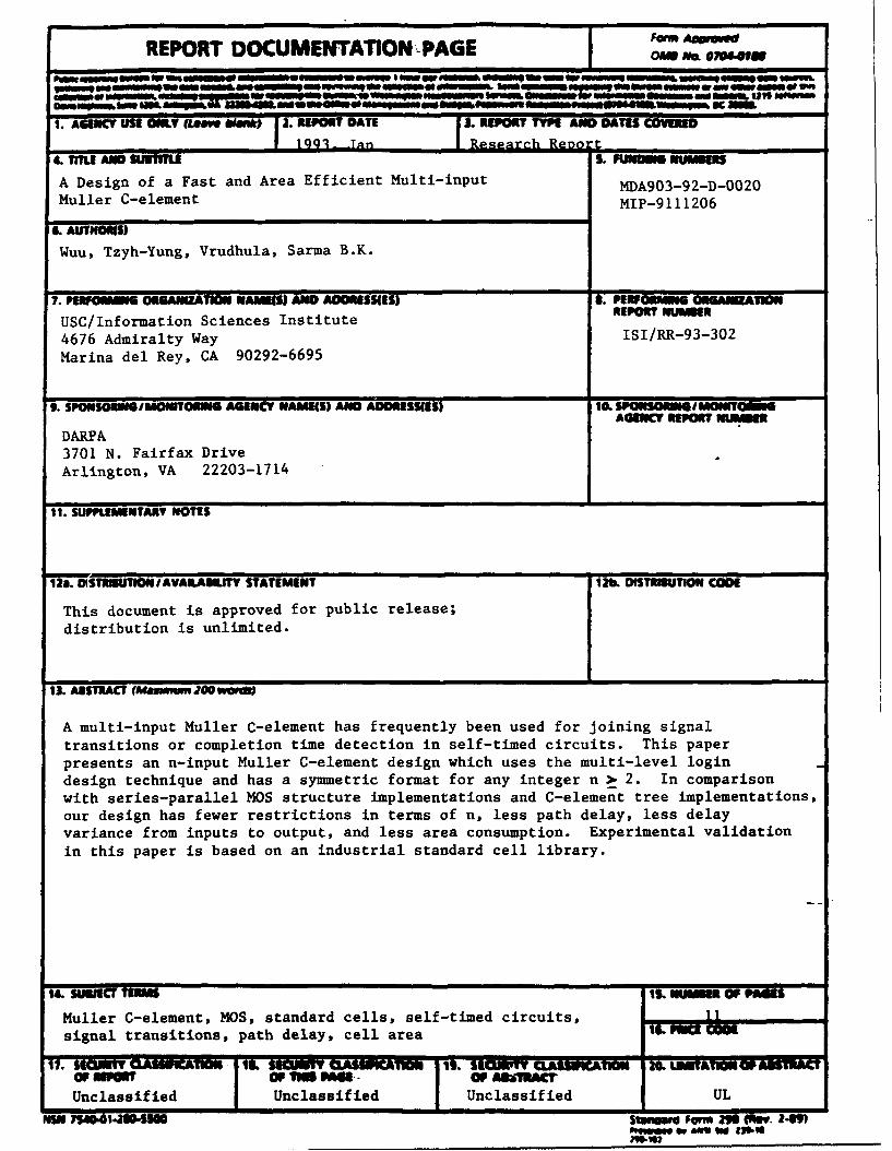
REPORT DOCUMENTATION PAGE Fn
isIII I lip ft a " Nom a to" o""*NNWt WWO4~amof Ic Owgmm
1. AGENCY USE ONLY (Loo &1&*) 2. REPORT DATE J. RE1PORT TMP AND DATE COVERED
17 9g,9 I T an IResearch Renar4. TITLE AND SUBIUI. UNNLNM@
A Design of a Fast and Area Efficient Multi-input MDA903-92-DO020Muller C-element MIP-9111206
4. AUITHOWS)W
Wuu, Tzyh-Yung, Vrudhula, Sarrna B.K.
7. PEWOMUISI ORGBANIATION NAMEES AND AOOUSS4ES)
USC/Information Sciences Institute IO NME
4676 Admiralty Way ISI/ RR-93-302
Marina del Rey, CA 90292-6695
I. SPONSORINSIMONITORIUS AGENC" NAUE4S) AND AOOIESS(ES) 10. SPONSOMINGIMONSTOSaAGENCY REOMT EMKIE
DARPA3701 N. Fairfax DriveArlington, VA 22203-1714
11. SUPPLEMENTARY NOTES
- I
128. A5TRinUTsONLAVALAWfIUTY STATEMENT 12b. DISTUTlON CONE
This document is approved for public release;distribution is unlimited.
13. ASITRACT (Maaxmum .00wam
A multi-input Muller C-element has frequently been used for joining signal
transitions or completion time detection in self-timed circuits. This paperpresents an n-input Muller C-element design which uses the multi-level login
design technique and has a symmetric format for any integer n > 2. In comparison
with series-parallel MOS structure implementations and C-element tree implementations,
our design has fewer restrictions in terms of n, less path delay, less delay
variance from inputs to output, and less area consumption. Experimental validation
in this paper is based on an industrial standard cell library.
IT SIW Tana IS. N4MMBI O
Muller C-element, MOS, standard cells, self-timed circuits, 11
signal transitions, path delay, cell area I1IL PUNCE CM
Arlinton, a to- 13. EO NWICAIO 1. SUA V20 3-171AII4U 2 2 T104 OP ANUACT
!I. SUPO•MITRT NOTES~IAC
Uclassified Unclassified isUnclassified Ua
N.N 7ABSTRI.AST ¢ :nw FM 2" 10ftm Wamy "dAre
MWisig
.BL INSTUMTONS FOR COMPLETING SIP 293jThe Report MocumentainPg (110M is used in announi ng and cataloging report. it is importantthat this information beconsistent with the rest of the report. particularly the cover and title page.Instructions for filling in each block of the form follow. It is important to stay wl"hh thme lines to meet
Block 1. Aaemt Use Only (Lemv blank) Block 12e. DistributionAvailabilitv ttmnBloc 2.Roo D&. Fll ublcaton ateDenotes public availability or limitations. Cite any
Bnlockn 2. y monthg. anll puliation dviatle gI availability to the public. Enter additionalincldin day moth, nd ear if vaiable(e~. ~ limitations or special markings in all capitals (e.g.
Jan 88). Must cite at least the year. NOFORN. REL. ITAR).
Block 3. Type of Renor arid Date Covered DOD -See DoDD 5230.24,. DistributionState whether report is interim, final. etc. IfStemnsoTchiaapplicable, enter inclusive r eport dates (e.g. 10 Statulements o ehia
Jun 7 - 0 Ju 84.DOE - See authorities.Block 4. Tile and Subtitl A tifte is taken from NASA - See Handbook NHB 2200.2.the part of the. report that provides the most NTIS - Leav blank.meaningful and complete information. When a0report is prepared in more thani one volume. lc b isrbto oerepeat the pnmarytitle. add volume number,. and Blclb.DsrutoCd.include subtilea for the specific~volume. On 00-Lmbakclassified documents enter the tifte classification DOE - LEaver blank.iutoncteore
in paenthses.from the Standard Distribution forBlock 5. Fu~n Nmm To include contract Unclassified Scientific and Technicaland grant numbers; may include program Reports.
ement number(s). project numberds), task NASA - Loom blank."umber(s), and work unit number(s). Use the NTIS - Leav blank.following labels:
C -contract PR - PrOect Block 13. Include a brief (MlaximumG -Grant TA - Task 200 words) factual summary of the mostPE Program WU - Work Unit significant informatior contained in the report.
Element Accession No.
Block S. ~Authors) Name(s) of person(s) Block 14. SubjsioctTems Keywords or. phrasesresponsible for writing the report pwiforming identifying major subjects in the report.the research. or credited with the content of thereport. if editor or compiler, this should followthe name~s). Block I15. Number of Pg=e. Enter the total
number of pages.Block 7. Performina Oroaniuation Namer(s) andAdrsfs Self-explanatoty. Block'16. PrisgCgdg. Enter appropriateprcIloick 2. Petri raiainRpn code (NTI only).
~.Enter the unique alphanumeric reportnumbrs) assgned by the organization Bkk 17. -19. Security Classifications. Self-performing the rpot explanatory. Enter U.S. Security Classification in
Blc 9 pnsrnafoitrnaamNaes accordance with U.S. Security Regulations 0(i.e.and ddrssle). elfexplnatry.UNCLASSIFIED). If form contains classified
information, stamp classification on the top andBlock 10. SoomodefifahdeAaec bottom of the page.Reor (if known)
Block 11. Sunse GEtrBlock 20. Limitation- of Atac.This block must0infanatone not' dncuded esenwhere such as: be completed to assign a limitation to thePrep@Med in cooperati don with ... ; Trans. of ...; To be abstract. Enter eitherUL (unlimnite) or SAR (samepubluidmed In.... Whla repor is revised. include- as report). An en"y in fths block ft -necessarr ifa statumen whethewr teew report supersedes the abstract is to be limitd If blank, the abstractor supplemients the older .epamt is aginmed o beunlImited
StMar 11- n 11 F0111 M 11t W, 249)
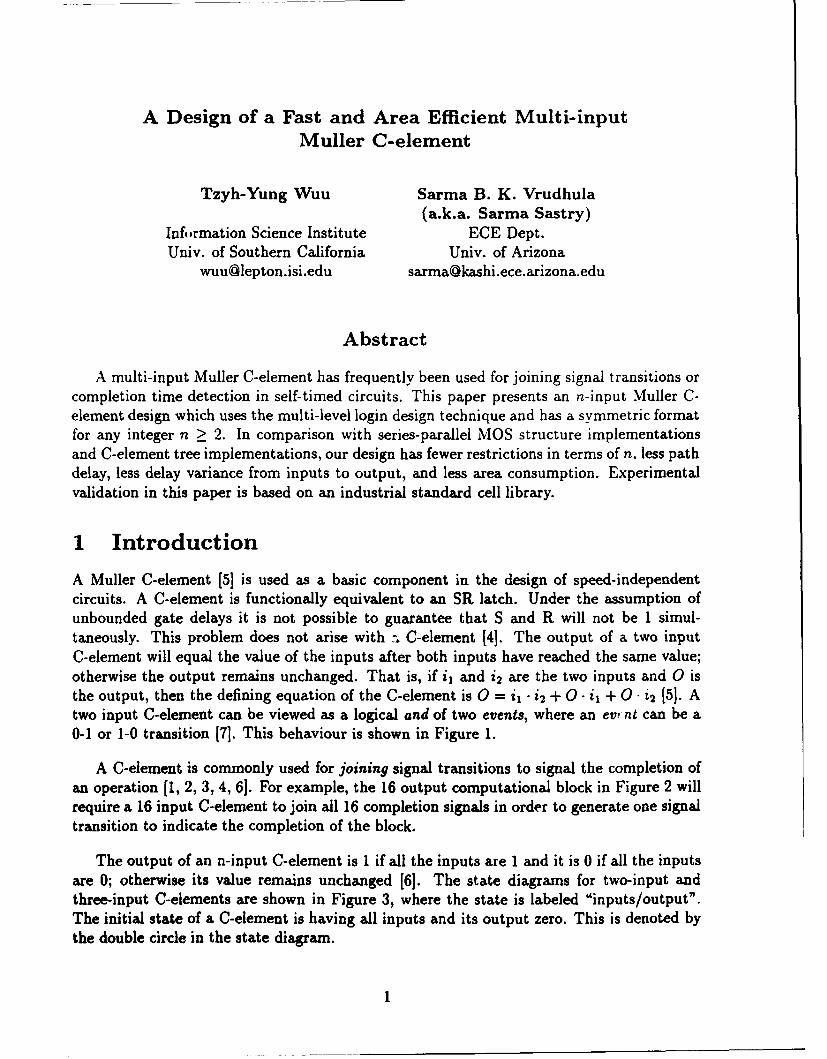
A Design of a Fast and Area Efficient Multi-inputMuller C-element
Tzyh-Yung Wuu Sarma B. K. Vrudhula(a.k.a. Sarma Sastry)
Information Science Institute ECE Dept.Univ. of Southern California Univ. of Arizona
[email protected] [email protected]
Abstract
A multi-input Muller C-element has frequently been used for joining signal transitions orcompletion time detection in self-timed circuits. This paper presents an n-input Muller C-element design which uses the multi-level login design technique and has a symmetric formatfor any integer n > 2. In comparison with series-parallel MOS structure implementationsand C-element tree implementations, our design has fewer restrictions in terms of n. less pathdelay, less delay variance from inputs to output, and less area consumption. Experimentalvalidation in this paper is based on an industrial standard cell library.
1 Introduction
A Muller C-element (5] is used as a basic component in the design of speed-independentcircuits. A C-element is functionally equivalent to an SR latch. Under the assumption ofunbounded gate delays it is not possible to guarantee that S and R will not be 1 simul-taneously. This problem does not arise with -. C-element [4]. The output of a two inputC-element will equal the value of the inputs after both inputs have reached the same value;otherwise the output remains unchanged. That is, if il and i2 are the two inputs and 0 isthe output, then the defining equation of the C-element is 0 = ii • i2 + 0- i1 + 0 - 2 [5]. Atwo input C-element can be viewed as a logical and of two events, where an evw nt can be a0-1 or 1-0 transition (7]. This behaviour is shown in Figure 1.
A C-element is commonly used for joining signal transitions to signal the completion ofan operation [1, 2, 3, 4, 6]. For example, the 16 output computational block in Figure 2 willrequire a 16 input C-element to join all 16 completion signals in order to generate one signaltransition to indicate the completion of the block.
The output of an n-input C-element is 1 if all the inputs are 1 and it is 0 if all the inputsare 0; otherwise its value remains unchanged [6]. The state diagrams for two-input andthree-input C-elements are shown in Figure 3, where the state is labeled "inputs/output".The initial state of a C-element is having all inputs and its output zero. This is denoted bythe double circle in the state diagram.

US
i/0
Figure 1: Timing diagrams for 2-input Muller C-elements
Self-timed dOQ,. i na - '•
Block " d15 d . >"
(a) A typical self-timed computational block
--- La- of all remt Sigils
* ~L"s of nil COMm)OdSiraU-si
* a
(b) rting diagsrm of the coWpletinrse signals
Figure 2: Join of completion/reset signals
2

0000/0
10/6 1/
11/0
11/1 1/ 10/ 11 1
00/1T/
(a) Two-input C-element (b) Three-input C-element
Figure 3: State diagrams for Muller C-elements
3C
00(a) Series-parallel MOS structure (b) C-tree structure
Figure 4: Three-input series-parallel C-element designs
I Availability CodesMWYC QUALIM INSPEMCTD 3 vat /
3special3A
,(I _ _I - - _

C-elements with large numbers of inputs are very useful and an efficient implementationin terms of area and speed is needed. Two designs of multi-input C-elements have been used;a series-parallel MOS structure [6] shown in Figure 4(a) and the C-element tree [4, 6] shownin Figure 4(b). Because the C-element is associative, the tree implementation uses (n - 1)two-input C-elements to form an n-input C-element. The input-output delay of the series-,parallel MOS structure is less than that of the tree structure. However, the series-parallelimplementation is not feasible for large n. For this reason, most existing designs employ thetree structure. The main disadvantages of the tree implementation are that it is very slowand the variance in the delays over different input-output paths is very large.
In this paper we present an efficient design of a multi-input C-element. Our design issymmetric and the variance in delay over different input-output paths is very small. InSection 2 we derive a symmetric form of an n-input C-element and provide estimates ofdelay and area. In Section 3 we demonstrate the advantages of our design by presentingexperimental results for C-elements with inputs ranging from 2 to 128.
2 Design of a Multi-input C-element
The target technology of our design is CMOS. Since inverted logic is faster than non-invertedlogic in CMOS, we will use and-or-invert (AOI) logic and inverters instead of and-or logic.The defining equation of an n-input C-element with a reset is given by
OUT = ((Ih * I 2 .... In) + (I + I 2 +... + In)oOUT)o RESET (1)
where Ii, for i = 1,...,n, are inputs of the C-element, and OUT is the output of the
C-element. Using DeMorgan's law we transform Equation (1) as follows:
OUT = ((1, *12 .... I) + (h + 12 +... + I). OUT) 9 RESET (2)
= ((h.oI 2 ... *In)+(I,+2 +...+In)oOUT).RESET
= ((I 1 .I 2 .... o In) +O(I 1 2 +.In).O UT) + RESET
= (h.I 2oo...9In,)o(I,+1 2 +...+I,,)oOUT+ RESET
= (, e h1 *... e In) ((I 2 + . + I,) + -U-T) + RESET (3)
Equation (3) can be further decomposed to following equations. 0
NANDTREE = (1,* 12 ... In) (4)
NOR.TREE = (+I2 +... + I) (5)
OUT = NANDTREE * (NOR-TREE + OUT) + RESET (6)
4

1w - NOR-TREE
12
In Q
o OAO_PARTOU
NAVDTREE
Figure 5: C-elements design
0 019 19
1i14
(a) Two-level NANDTREE implementation
12 B12B
OUT 0 a OUT>0CID_.. 0 00F__ 0
In 1.IL3
(b) Three-level NANDTREE implementation
Figure 6: Multi-level NANDTREE implementation
5

The above decomposition is very useful when it is mapped to a CMOS cell-based imple-mentation. In Figure 5 we show a C-element design consisting of 3 parts: a NANDTREE, aNOR-TREE, and a OAOPART (or-and-or), each implemented separately. The OAOPARTshown in Figure 5 remains the same for all values of n.
Therefore, we only need to find a proper NANDTREE/NORTREE implementation. Inthe HP C34000 library [81, there are n-input NAND and NOR gates for 2 < n < 8. Forlarger n, NANDTREE (NOR-TREE) can be further decomposed into two-level NAND-ORtree (NOR-AND tree). When a two-level structure is not sufficient, we can use more levels,i.e., use a nand-nor-nand three level structure to implement a NANDTREE or a nor-nand-nor structure to implement a NORLTREE. Figures 6 (a) and (b) show the two-level andthe three-level implementations for NAND.TREE. In order to minimize the variance of theinput-output delays, the structure of the NANDTREE implementation is identical to thestructure of the NOR. TREE implementation.
We now provide estimates of delay and area for our design and compare them with thetree implementation of a C-element. A comparison with a series-parallel MOS structure isunnecessary since such an implementation is not feasible for large numbers of inputs.
Delay: For an n-input C-element, the input-output delay of a C-element tree implemen-tation is equal to the number of levels in the structure multiplied by the input-output delayof a 2-input C-element, where the number of levels is [log2 n], i.e.,
Dee,.(n) = [log2n] * ( 2-input Muller C-element delay ) (7)
;t [log2n] * ( 2-input NAND/NOR delay + OAOI delay) (8); flog2n] * OAOI delay + [log2n] * 2-input NAND/NOR delay
The input-output of our design is .
Dmuti(n) = OAOI delay + n-input NANDTREE/NORTREE delay (9)
The n-input NAND.TREE/NOR.TREE can be implemented by [log2n] stages of a NAND2-NOR2 tree, and can be made faster by using [logn] stages of NANDm-NORm tree. There-fore,
Dmati(n) <_ OAOI delay + [log2 n] * 2-input NAND/NOR delay (10)
ehviously, our design is much faster than C-element tree implementation for n > 2, althoughboth Dt...(n) and DmIti(n) are O(log(n)).
Delay Variance: In order to have less delay variance among the input-output paths inour design, two sufficient conditions need to be met.
1. Transistors in the OAOI element of 1he OAO.PART must be sized so that the delayfrom one OR gate input to the output and the delay from one AND gate input to the •output is the same.
6
S. .. .

2. the structure of NANDTREE should be symmetric and identical to the structure ofthe NOR.TREE.
These two conditions are easily satisfied for cell-based designs, and they are a property ofthe HP standard cell library. However, the tree implementation of an n-input C-element isbalanced only if n = 2F1 9g211. For this reason, the variation in delays among the differentinput-output paths is very large.
Area: In comparing our design with the C-element tree implementation, the routing areais not considered. Similar to the delay comparison above, the C-element tree has a bigoverhead in terms of size due to the repeated use of the OAO.PART in every two-inputC-element in the tree. An estimate of the area of a C-element tree implementation is
Atr,,f(n) ; (n - 1) * (ANAND2 + ANOR2 + AoAoI + AINV) (11)
,z (n - 1) * (AoAoI + AINv) + (n - 1) * ANAND2 + (n - ) ANOR2
The estimate of area for our design is
Amuiti(n) -- AoMot + AiNv + An.input NANDTREE + A n-input NOR-TREE (12)
The n-input NANDTREE/NOR.TREE can be implemented by (n - 1) number of NAND2-NOR2 elements, and it may have a similar sized implementation by using [logn] stages ofNANDm-NORm tree. Therefore,
Amuti(n) -_ Ao0oj + AINV + (n - 1) * ANAND2 + (n - 1) * ANOR2
Obviously, our design is much smaller than C-element tree implementation for n > 2, al-though both At,...(n) and A.u.ti(n) are 0(n).
3 Experimental results
We present experimental results using the HP C34000 standard cell library (8]. The input-output path delay is obtained by simulating a VerilogTM I model distributed with this celllibrary. Wiring capacitances are included in the model. For each n-input C-element, boththe rise and fall delays for all input-output paths are simulated, i.e., 2n path delays arecollected. The path delay of an n-input C-element is taken to be the average of these 2ndelays. The delay variance among input-output paths is calculated by the difference betweenthe maximum input-output path delay and the minimum input-output path delay of allinput-output paths. The area of a design is computed as the sum of the area of all cells inthe design. The results are shown in the Table 1. In this table, the name of Muller C-elementsuffixed with "A" is the series-parallel structure implementation, the name suffixed with "B"is our design, and the name suffixed with "AT" is the C-element tree implementation using"mullerC2AW, and the name suffixed with "BT" is the C-element tree implementation using"UmullerC2B".
'Verilog is a hardware description language, and it is a trademark of Cadence Design Systems, Inc.
7

min (nsec) max (nsec) avg (nsec) max - min (nsec) I area (p2)
mullerC2A 2.8 3.6 3.2 0.8_ 3319_ _
mullerC2B 2.9 J.2 3.0 0.3 4085mullerC3B 3.0 3.1 3.1 0.1 4596mullerC4B 3.0 3.3 3.1 0.3 5107mullerC5B 3.0 3.5 3.3 0.5 5874mullerC6B 3.9 4.5 4.1 0.6 6384mullerC7B 3.9 4.8 4.2 0.9 6894mullerC8B 3.9 4.6 4.2 0.7 7661mullerC9B 3.9 4.4 4.1 0.5 6384mullerC16B 3.9 4.4 4.2 0.5 16343mullerC32B 4.2 4.8 4.6 0. 32175mullerC64B 4.4 4.9 4.6 0.5 61287mullerC128B 5.3 6.0 5.6 0.7 122063
mullerC2AT 2.8 3.6 3.2 0.8 3319mullerC3AT 2.8 7.9 5.9 5.1 6638 0mullerC4AT 6.0 7.9 6.9 1.9 9957mullerC5AT 6.4 12.1 8.6 5.7 13276mullerC6AT 6.5 12.1 9.6 5.6 16595mullerC7AT 6.0 12.1 10.2 6.1 19914mullerC8AT 9.3 12.1 10.6 2.8 23233 •mullerC9AT 9.7 16.3 11.7 6.6 26552mullerC16AT 12.5 16.3 14.4 3.8 49785mullerC32AT 14.5 20.0 17.9 5.5 102889mullerC64AT 19.0 24.7 21.7 5.7 209097mullerC128AT 22.3 28.9 25.4 6.6 421513 0
mullerC2BT 2.9 3.2 3.0 0.3 4085mullerC3BT 3.2 7.4 5.9 4.2 8170mullerC4BT 7.2 7.6 7.4 0.4 12255mullerC5BT 7.1 11.6 9.0 4.5 16340mullerC6BT 7.5 11.9 10.3 4.4 20425mullerC7BT 7.5 11.8 11.1 4.3 24510mullerC8BT 11.4 12.0 11.7 0.6 28595mullerC9BT 11.5 15.8 12.6 4.3 32680
mullerC16BT 15.7 16.5 16.1 0.8 61275mullerC32BT 19.9 21.1 20.4 1.2 122635mullerC64BT 24.1 25.6 24.7 1.5 257355mullerC128BT 28.3 30.1 29.1 1.8 518795
Table 1: Delay and delay variance and area comparisons of Muller C-element 0
8

Figure 7 shows the path delays in terms of 1og 2n. As expected, the path delay of theC-element tree is approximately equal to [log2n] * K, where K is the delay of a 2-inputC-element including wiring delay. Our design is much faster than the C-element tree im-plementation, and path delay grows very slowly as n increases. For example, our 32-inputC-element design is 3.89 to 4.43 times faster than C-element tree design. Figure 8 shows thedelay variance among input-output paths in terms of n. The delay variance of our design issmall for any number of inputs, but the delay variance of the tree implementation is onlysmall for a balanced tree, i.e., where n = 2r[,g2nl. Finally, the area comparison between ourdesign and the C-element tree implementation is shown in Figure 9. In both our design andC-tree implementation, the cell area grows linearly with n. However, the increasing areain our design is due to its NANDTREE and NOR-TREE whereas the increasing area forthe C-element tree implementation is due to the number of 2-input C-elements. Therefore,the rate of increase of area for our design is much smaller than for the tree implementa-tion. For example, our 32-input design is 3.20 to 3.81 times smaller than the C-element treeimplementation.
30: MullerwcB
c: MuluSCPAT
~2O .x -M• ,25 .... .. .
10.r
1 2 .............................. .................. . ........... .... ........ ......... .. . ..... ... ..... ..:- .... ..... ..." .' .......... ..... .... ..... ....
10~~~~~ ~ ~ ...................... . ....... .......... o....... .............
.. .. oo1 .• .... .... .... ........ .... ..................... .................... ..... i. ,•. ........ . .. ... ................... .............................
'( ~ ~ ... .... F".. l• :..
0 .1 2 3 4 5 6 7
Number of bnpU (Iog2 n)
Figure 7: Comparison of path delay
9

:MUIleICnB0o: MuilcCnAT
6 .x: .M uldIe.Cn.BT .......9...... ..........~ ~ ~ .....-. ... .. ..
5 .... ................ ........ ................... ........
4 . ....... ... ... .. ... .. .. .. .. . .. .. . .. .. . .. .. ... ... . .. .... . .. .. .. .. W
00
Number of inputs (n)0
Figure 8: Comparison of delay variance
X1006
o: MullexCuATx ý;:.M ~uiezC~nB.T ........................ ... ........
4 ............. .. ........ ..... ..................... ............. ....... .... ..... .0..
.... ... 0.
0
0 20 40 60 so 100 120 140
Number of inpat (n)
Figure 9: Comparison of cell area
10

4 ConclusionsWe have presented a new design for an n-input C-element. which is faster. has less delayvariance among input-output paths, and is smaller than the C-element tree implementation.We have also demonstrated the advantages of our design using an industrial standard celllibrary.
Acknowledgement
The authors thank the MOSIS group at USC-ISI for the netlist-to-parts service, the useof the standard cell library, and the implementation tools.
References
[1] E. Brunvand and R. F. Sproull. Translating Concurrent Communicating Programs intoDelay-Insensitive Circuits. Technical Report CMU-CS-89-126. School of Computer Sci-ence, Carnegie Mellon University, April 1989.
1[2] I. David, R. Ginosar, and M. Yoeli. "An Efficient Implementation of Boolean Functions
and Finite State Machines as Self-Timed Circuits". ACM Computer Architecture News.17(6):91-104, 1989.
0 [31 A. J. Martin et al. The Design of an Asynchronous Microprocessor. Proceedings of theDecennial Caltech Conference on VLSI, pages 351-373, March 1989.
[41 T. H.-Y. Meng. Synchronization Design for Digital Systems. Kluwer Academic Publish-ers, 1991.
S([5] D. E. Muller and W. S. Bartky. "A Theory of Asynchronous Circuits". Proceedings ofan International Symposium on the Theory of Switching, 29:204-243, 1959.
[6] C. L. Seitz. "System Timing". In Introduction to VLSI Systems. by C. Mead and L.Conway, Addison Wesley, pages 128-262, 1980.
[7] I. E. Sutherland. "MICROPIPELINES", The 1988 Turing Award Lecture. Communica-
tions of the ACM, 32(6):720-738, 1989.
[81 The HP C34000 Standard Cell Library Data Manual (Draft). Hewlett-Packard Company,Integrated Circuit Business Division, June 1992.
11