Yearbook · Makyoh topography.....43 Determination of migration of ion -implanted Ar and Zn in...
138
Yearbook 2015 1 Yearbook 2015 Institute of Technical Physics and Materials Science http://www.mfa.kfki.hu/ Hungarian Academy of Sciences Centre for Energy Research
Transcript of Yearbook · Makyoh topography.....43 Determination of migration of ion -implanted Ar and Zn in...
Yearbook 2015
1
Yearbook
2015
Institute of Technical Physics
and Materials Science
http://www.mfa.kfki.hu/
Hungarian Academy of Sciences
Centre for Energy Research

2
Institute of Technical Physics and Materials Science Director: Prof. István Bársony, corr. member of HAS Address: Konkoly-Thege Miklós út 29-33, H-1121 Budapest, Hungary Postal: P.O.Box 49, H-1525 Budapest, Hungary Phone: +36-1-392 2225 Fax: +36-1-392 2226 E-mail: [email protected]
URL: http://www.mfa.kfki.hu/
MTA EK MFA Yearbook 2015 Editor: Csaba S. Daróczi Published by: MTA EK MFA, Budapest, Hungary, 2015

Yearbook 2015
3
CONTENT Content ..................................................................................................................................... 3 Director’s Foreword ................................................................................................................. 5 General Information ................................................................................................................. 8 Organisation of MFA .......................................................................................................... 8 Key Financial Figures.......................................................................................................... 9 Publications and Citations ................................................................................................. 10 Awards and Distinctions .................................................................................................... 12 Highlights ............................................................................................................................... 14 Wafer-scale integration of piezoelectric nanowires ...................................................... 14 Nanoparticle assemblies ............................................................................................... 17 Notable Events ....................................................................................................................... 20 Public Outreach ...................................................................................................................... 23 Scientific Reports ................................................................................................................... 26 Nanostructures Laboratory ................................................................................................ 26 Exfoliation of large-area transition metal chalcogenide single layers .......................... 27 Structure and properties of graphene on gold nanoparticles ......................................... 29 Electronic properties of MoS2 flakes grown on graphite .............................................. 31 Atomic and electronic structure of native point defects in MoS2 single layers // ......... 33 Modulation of physical properties by stacking of 2D materials ................................... 35 Variability of structural coloration in blue butterfly wings .......................................... 37 Photonics Department ....................................................................................................... 39 Nondestructive indication of fatigue damage in ferromagnetic construction // ............ 41 Makyoh topography...................................................................................................... 43 Determination of migration of ion-implanted Ar and Zn in silica by // ........................ 44 Verification of the effective medium approximation for surface roughness by // ........ 45 Plasmon-enhanced two-channel Kretschmann ellipsometry ........................................ 46 Protein adsorption, cell adhesion and polyelectrolyte deposition on titania // .............. 47 Development of optical metrology tool for in-line qualification of thin films on // ..... 49 Preparation of compact nanoparticle clusters from polyethylene glycol-coated // ....... 50 Introducing nanoscaled surface morphology and percolation barrier network into // .. 52 Effect of heat treatments on the properties of hydrogenated amorphous silicon for // . 54 Microtechnology Department ............................................................................................ 55 MEMS .......................................................................................................................... 58 Fine-tuning of gas sensitivity by modification of nano-crystalline WO3 // ............. 58 Wavelength conversion in GaInAsP/InP near infrared surface emitting diodes //... 60 3D force sensors for minimal invasive surgery applications ................................... 62 Modeling and Simulation @ MEMS Lab ................................................................ 64 3D interpolated potential for MD ............................................................................ 65 Nanosize effect on the evolution of magnetism on curved surfaces ........................ 66 BioMEMS .................................................................................................................... 68 Microfluidic system for separation of circulating tumor cells (CTC)...................... 68 Finite Element Modeling (FEM) and characterization of cell and molecular // ...... 70

4
Autonomous microfluidic sample transport systems ............................................... 72 Cell and particle sorting in microfluidic systems .................................................... 74 NeuroMEMS ................................................................................................................ 76 Silicon probes designed for infrared neural stimulation .......................................... 76 Iontophoretic injection microsystem delivering pathway tracer molecules in // ..... 77 Polymer microECoGs optimized for in vivo pharmacological investigations ......... 78 In vitro studies revealing the immune response of the living tissue to // ................. 80 NEMS ........................................................................................................................... 81 Homogeneous transparent conductive ZnO:Ga by ALD for large LED wafers ...... 81 Double Markers for Direct Contact Formation on Ultra-Low Dimension Objects . 83 Thin Film Physics Department .......................................................................................... 85 New approaches in the development of Hypoallergenic implant material in // ............ 86 Characterization of biocompatible ceramic TiC / amorphous C thin films prepared // 87 Graphene-ceramic composites for tribological application in aqueous environments . 88 Low cycle thermomechanical fatigue of a reactor steel: microstructural // .................. 90 Characterization of defect structure in electrodeposited nanocrystalline Ni films ....... 92 Characterization of the topography of the graphene moiré superlattice on // ............... 93 Microscopy of high quality cubic SiC grown on Si ...................................................... 95 Metal (Ni) induced crystallization in amorphous Si thin films ..................................... 96 A universal nanopatterning technique using RF plasma etching through templates // . 97 CoPt/TiN thin films of enhanced perpendicular coercivity by N2 // ........................... 100 A device for micro-combinatorial TEM studies ......................................................... 101 Grain boundary characterization based on diffraction data ........................................ 103 Nanobiosensorics „Lendület” Research Group ............................................................... 106 Hydrogel film fabrication for biosensing ................................................................... 107 Label-free profiling of cell adhesion: Determination of the dissociation constant // .. 108 Incubator proof miniaturized Holomonitor to in situ monitor cancer cells exposed // 109 Biophysical characteristics of proteins and living cells exposed to the green tea ....... 111 Automated single cell isolation from suspension with computer vision..................... 112 Monitoring of cellular toxicity assessment of agrochemicals by using label-free // ... 114 The dynamics of living cell adhesion on nanostructured genetically engineered //.... 115 Complex Systems Department ........................................................................................ 116 Does knowing the opponent's strategy guarantee optimal play? ................................ 117 Eurasian mtDNA analysis with a new iterative rank-correlation method ................... 118 Griffiths phases and localization in hierarchical modular networks ........................... 120 MFA Seminar Talks ........................................................................................................ 121 Research and Development Partners, Foreign Visitors ................................................... 123 MFA Publications in 2015 ............................................................................................... 125

Yearbook 2015
5
DIRECTOR’S FOREWORD
Struggling to survive a difficult year of adaptation… the
Institute of Technical Physics and Materials Science in
2015 completed the first year as administratively part of
the Centre for Energy Research (EK). We can call
ourselves fortunate because of the timely escape from the
large centralised organisation of the Research Centre for
Natural Sciences (TTK), which in 2015 effectively was
declared bankrupt, reporting a huge loss of funds due to
mismanagement and bad operation. The long-sought
decision of the Presidium of the HAS to detach MFA from
that Centre in 2014 meant at the same time to integrate MFA administratively into the
current Centre (EK) operating on the KFKI Campus. Based on the experience of a
year of marriage we can summarise: this integration became a multicultural approach.
The predecessor of the EK centre was established as an engineering-type backup of
the Hungarian nuclear power plant in Paks, maintaining special skills and stand-by
R&D services next to training activities. “Academic type research”, according to the
criteria of which the performance of MFA is evaluated in the research network of the
HAS, was only a minor part of the EK centre’s activity, which drastically changed
with the forced integration of MFA. This imbalance is also expressed in the number
and qualifications of researchers in fission-related and materials research. The
difference in types of activities, or research cultures, obviously requires a different
administrative treatment. While the nuclear-type projects mostly have mid-term
financing stability owing to well-funded engineering development contracts, materials
research at MFA has to collect its funding from a large number of international and
national collaborative projects prone to severe EC restrictions in reporting and
accounting. While the large experimental nuclear facility historically enjoys
substantial dedicated funding from the HAS for its operation as a European research
facility, the large microtechnology infrastructure of MFA receives no central subsidy
whatsoever. Therefore, the latter research activity requires large flexibility in
management and administration to cope with the chronic lack of resources, to create
motivation for the researchers to initiate projects and partnerships in research
consortia and industrial collaborations.
So far, just the opposite happened as it turned out. The expected „unification of
standards and regulations” (in research and administratively, e.g. wage levels,
bonuses, etc.) in both parts of the expanded centre was not even attempted. Instead,
the director-general and the administrative director, bearing full responsibility for the
operation of the centre, did not delegate any, even minor, responsibility and
competencies for the director of MFA. As everything requires the signature of the
director-general and, more importantly, the approval of the financial director, the
MFA director’s function became just symbolic in this atmosphere of distrust. The

6
centre management did not consider it important to involve the research leaders of the
institute in strategic or operative decisions; so far, even upon request, no regular
information is being provided about the financial situation in individual projects,
support received, scheduling of MFA procurements, payment of bills, liquidity of the
institute as a whole despite many promises. In order to signal these anomalies to the
elected leaders of the Academy, in summer 2015 one of our department leaders
volunteered to submit a formal application for the position of the director-general, in
which he openly criticised the malfunctioning of the management. The Presidium,
however, prolonged the assignment of the present director-general for another five
years.
Even in these difficult circumstances MFA in 2015 again recorded a successful year,
marked by excellent scientific results and accomplishments, as presented in this
booklet.
We only can hope that the survey and fine-tuning of the current centralised research
network announced by the President of the HAS will result in a more democratic,
transparent and efficient regime in the research centres. The advocated restoration of
most of the “freedom of action” enjoyed still five years ago, is hopefully going to
ease the life of the new MFA leadership under my successor.
When becoming the director of the at that time independent Research Institute for
Technical Physics and Materials Science in 2004 I had a clear vision about the
midterm research strategy and goals and how to achieve them. In my application for
the assignment I built upon the SWOT analysis of the Institute and defined the major
priorities for materials research at MFA: a complete nanoscience and –technology
focus; more opening towards biology to enhance multi-disciplinarity; improve the
scientific qualification of researchers; and drastically reverse the age-distribution of
the staff.
After twelve years one can state with satisfaction that most of those targets could be
achieved. Although the socio-economic landscape world-wide, in the country and
within the Academy changed a lot, MFA had a prosperous decade, before having
been forced under centralised administrations. The Institute still works under the
Quality assurance system ISO 9000-2008. The annual MFA Yearbooks published in
English document the history of development of „MFA as a research community”
(available in print and electronically at http://www.mfa.kfki.hu/hu/yearbook).
The scientific part is a summary of most important research results from the previous
year, as presented at the end of January each year on the annual „scientific reporting
day” of MFA, where the opinion of external reviewers - mainly from prospective co-
operating institutions - is also asked for. The Yearbooks also give an account of
successful initiatives, like the “MFA Summer School” for high school children from
the Carpathian Basin, team-building events like the yearly „MFA-Day”, the
“Christmas celebration”, and the raising of awareness for our research in different
popular actions, which in the meantime were adopted also by others. These occasions

Yearbook 2015
7
provided the forum for motivation of our staff by handing out the „MFA Prize” in
three categories and the ”MFA Prize for Excellent Research Support”, as well as
the title “Professor emeritus instituti” for our retired scientific advisors. Whenever
it was possible, colleagues of our institute were promoted and recommended for
distinction by the HAS and by various national awards.
Just to mention a few representative figures from the last 12 years:
At least 8 new laboratories were built for the novel research activities started, and all
the other laboratories and working cabinets were completely renovated, the furniture
replaced and modernised, and the research equipment updated depending on
availability of resources. MFA successfully guided 47 students to the degree of
Ph.D. with 23 more on the way, the title of Dr. of HAS (D.Sc.) was achieved by 15
of our colleagues, and two became corresponding members of the HAS! These
achievements earned for our institute respect and appreciation in the academic
community expressed also by the Széchenyi Prize awarded to the director in 2015.
MFA as mosaic-word became a brand not only in Hungary, but also Europe-
wide in our field of activity. What is most important, it constitutes a solid scientific
base for the future of research of functional materials in Hungary.
When relinquishing the director’s function, held for over 12 years, in the summer
2016, I have to thank all of my co-workers, especially my fellow research leaders, for
their excellent collaboration. I wish the new generation mastery in all future
challenges with bright new ideas and initiatives, by maintaining the MFA team spirit I
was fortunate to experience.
Budapest, March 1st, 2015
István Bársony
8
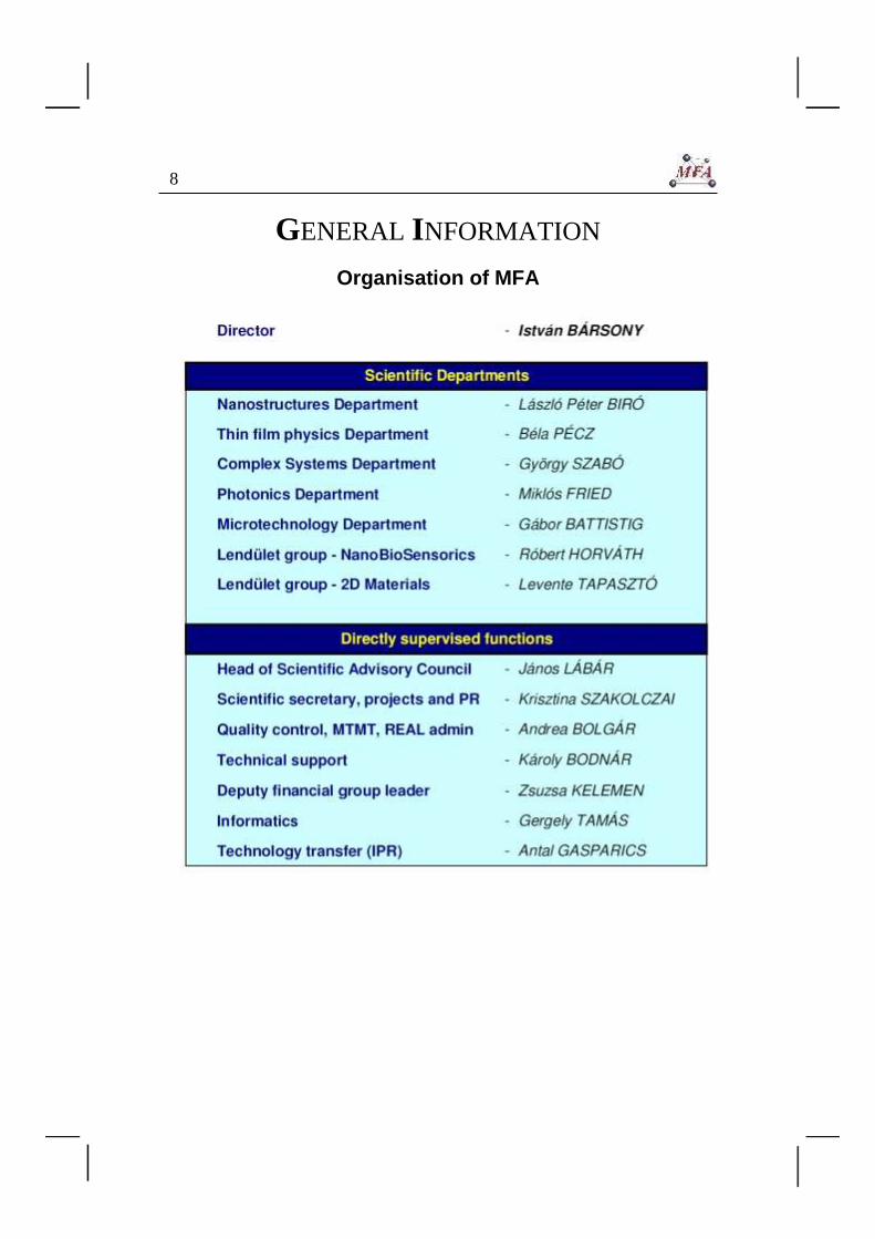
GENERAL INFORMATION
Organisation of MFA

Yearbook 2015
9
Key Financial Figures
The turnover realised by the institute in the last 12 years provides a good overview
about the evolution of the economical-societal circumstances around research and
development at an academic research institute, reflected by the composition of the
source of income, and the changes therein: the decrease of the central subsidies, the
role of international grants prone to the periodicity in the European Commission’s
and project support schemes, the situation in the domestic R&D financing (largely
bound to the EU cohesion- and structural funds), and the contract research -
characteristic for the industrial landscape in the country.
Until 2012 MFA was operating as an independent entity with a staff of 130, including
completely independent, but competent administration. All decisions were taken in
reasonable time and there was considerable freedom of decision granted to the
director having full responsibility for his decisions. The integration wave in the
research network of the HAS started from 2012.We lost our independence becoming
part of the 650 strong Research Centre for Natural Sciences (TTK). The increasing
costs of central administration meant parallel an operation of larger inertia, leading to
the drop in the performance of the same scientific staff. The decision of the Presidium
of the HAS taking MFA out of TTK and forcing it to integrate into the Centre for
Energy Research (EK) saved us from suffering by the bankruptcy of TTK, which
became obvious by early 2016. In the new host centre from 2015, due to the non-
transparent decision making and inefficient handling of our administration did not
improve much on our financial situation. By the lack of communication and
information flow, not to speak about the absence of trust as well as delegation of
competencies and responsibilities we do not have even access to authentic figures; the
data for 2015 are based upon our own estimates.
MTA EK MFA 2015 Budget Totals in Million HUF

10
MTA EK MFA 2015 restoration and investment spendings in Million HUF
We are confident that the 2015 figures reflect only a fraction of the performance,
MFA would be able to offer, provided a the young colleagues could be motivated to
enter more international and national collaborations, submit more proposals, and risk
much more endeavours with the industry.
Publications & Citations
Regarding scientific output, MFA produced a yearly average of 95-100 publications,
while continuously improving the record for citations.
MFA and its predecessors’ publications

Yearbook 2015
11
This was the case also in 2015, albeit the number of published papers in the calendar
year dropped to 80. This is on one hand caused by submission and evaluation delays;
on the other hand it reflects the complex administration problems we were prone to.
There is a remarkable trend to go for publications in higher profile periodicals hoping
for further significant improvement in the number of citations.
MFA and its predecessors’ citations

12
Awards & Distinctions
BÁRSONY, István
Széchenyi Prize by the President of Hungary
Distinguished Honorary Professorship by the National Institute of Technology,
Toyama College, Japan
SZABÓ, György Commander's Cross, Order of Merit of the
Republic of Hungary
DÜCSŐ,Csaba Knight's Cross, Order of Merit of the
Republic of Hungary
LOHNER, Tivadar ELFT Medal of the Roland Eötvös
Physical Society
BARNA, B. Péter
R. F. Bunshah Award of the International Conference on Metallurgical Coatings and Thin Films for his lifetime achievements
VONDERVISZT,
Ferenc
Golden Prize of the Veszprém Chapter of the Hungarian Academy of Sciences
SZOLNOKI, Attila „Outstanding Referee” award from
Physica A
FÜRJES, Péter MedinProt Synergy Research Program
(2014-2015) award

Yearbook 2015
13
BALÁZSI, Katalin Bolyai Plaquette of the Hungarian
Academy of Sciences
HORVÁTH, Róbert MFA Prize (Researcher)
LUKÁCS, István Endre MFA Prize (Postdoctoral)
OLÁH, Nikolett MFA Prize (Ph.D. student)
ILLÉS, Levente MFA Prize for Excellent Science Support
MENYHÁRD, Miklós Prof. Emeritus of the Hungarian Academy
of Sciences
GAÁL, István Professor Emeritus Instituti
MTA EK MFA
SZENTPÁLI, Béla Professor Emeritus Instituti
MTA EK MFA
Sotomi ISHIHARA
MFA prize for fostering a fruitful co-operation between KOSEN Toyama
College and MFA in various fields of S&T
Stefan LUBY
MFA prize for promoting the co-operation between our institute and the institutes of
the Slovak Academy of Sciences

14
HIGHLIGHTS
Wafer-scale integration of piezoelectric nanowires
(EU FP7 collaborative project 611019: PiezoMAT1)
I. E. Lukács, N.Q. Khánh, R. Erdélyi, Zs. Baji, G. Battistig, and J. Volk
The EU project PiezoMAT proposes new technologies of high-resolution fingerprint
sensors based on a matrix of interconnected piezoelectric nanowires (NWs). One of
the three targeted chip concepts was realized by the MFA team. Here the integrated
free standing vertical NWs are contacted individually at their stock with two metal
wires to detect piezoelectricity induced signals between tensed and compressed sides
of the NWs upon bending. As it was found by finite element analysis a nearly
constant positive/negative stress is built up in the outer/inner side of the NW upon
bending it by a lateral loading force directing to its tip (Figs. 1a and b). In contrast,
the induced piezoelectric potential has a strong maximum at the bottom of the NW
(Fig. 1c). The aim of this sensor concept is to detect this enhanced electrical signal
with a pair of metal electrodes contacting the opposite sides of the NWs at their roots.
Moreover, with an array of vertically integrated NWs, the distribution of the loading
force can also be detected at a very high (>5000 dpi) lateral resolution.
Figure 1 Finite element analysis of NW/seed layer/substrate assembly showing the ideal
meshing by triangular elements (a), cross-section of the zz component of the mechanical
stress (b), and the electric potential distribution (c) for the bottom part of the bent NW at a
loading force of 80 nN.
The optimization of the fabrication procedure was carried out through three stages, at
first on small (10 mm × 10 mm) sapphire dices, then on 3” sapphire wafer, and at last
on 3” Si wafer. The aim of the sapphire wafer is to realize ‘ideal’ monocrystalline
ZnO NWs on epitaxial ZnO seed layer, whereas that of the Si wafer is to demonstrate
1 FP7-ICT-2013-10- 611019 - High-resolution fingerprint sensing with vertical piezoelectric
nanowire matrices (PiezoMAT), www.piezomat.eu
Yearbook 2015
15
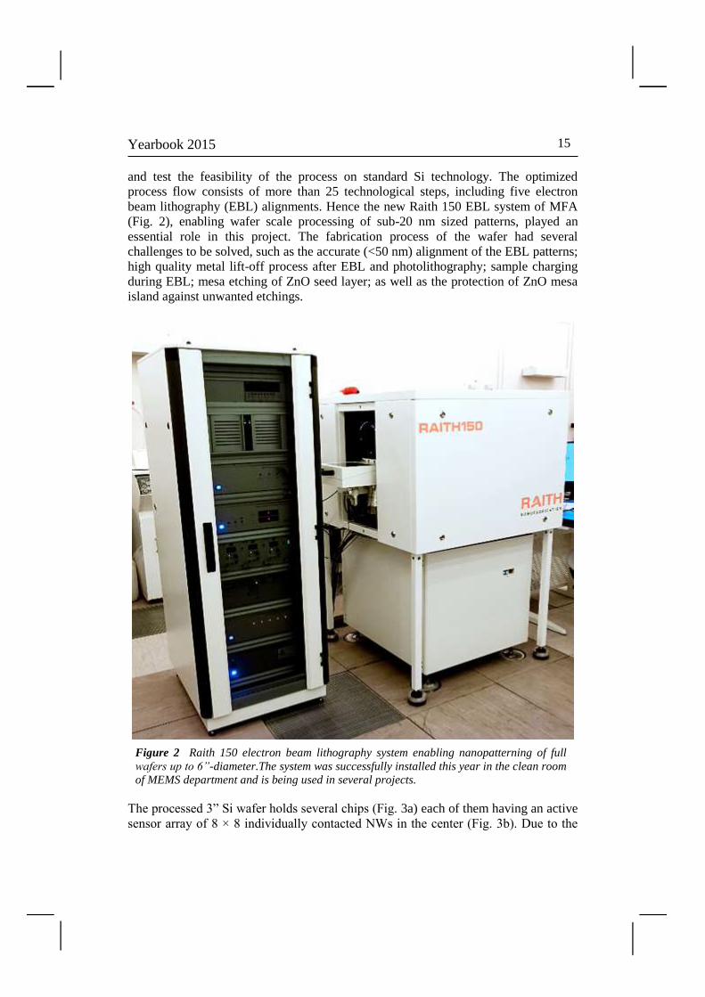
and test the feasibility of the process on standard Si technology. The optimized
process flow consists of more than 25 technological steps, including five electron
beam lithography (EBL) alignments. Hence the new Raith 150 EBL system of MFA
(Fig. 2), enabling wafer scale processing of sub-20 nm sized patterns, played an
essential role in this project. The fabrication process of the wafer had several
challenges to be solved, such as the accurate (<50 nm) alignment of the EBL patterns;
high quality metal lift-off process after EBL and photolithography; sample charging
during EBL; mesa etching of ZnO seed layer; as well as the protection of ZnO mesa
island against unwanted etchings.
Figure 2 Raith 150 electron beam lithography system enabling nanopatterning of full
wafers up to 6”-diameter.The system was successfully installed this year in the clean room
of MEMS department and is being used in several projects.
The processed 3” Si wafer holds several chips (Fig. 3a) each of them having an active
sensor array of 8 × 8 individually contacted NWs in the center (Fig. 3b). Due to the

16
high quality ZnO seed layer deposited at the University of Leipzig (ULEI) the ZnO
crystals show an excellent c-axis orientation even on the non-lattice matched SiO2
covered Si wafer. Nevertheless these NW transducers are polycrystalline (Fig. 3d) in
contrast to the ones grown on epitaxial ZnO/sapphire substrate (Fig. 3c). High
resolution SEM images revealed that the piezocrystals were positioned to the readout
contacts with sub-50 nm precision throughout the whole wafer (Fig. 3e).
Figure 3 On-chip integrated piezoelectric NWs. (a): Photo of Si wafer with NW chips,
(b): SEM image of the 8 × 8 NW array, (c and d, respectively): comparison of contacted
ZnO NWs grown on sapphire and Si substrate, (e): high magnification SEM image of the
contacted ZnO crystal where the read-out Au electrical lines are colored with yellow.
The electrical connections were verified by current-voltage (I-V) measurements using
a probe station and negligible crosstalk was found between the separate circuits. The
integrated NW chips are thus ready for the electromechanical characterizations which
will be carried out in two main steps. At first bending experiments will be done on
individual ZnO crystals with AFM and SEM micromanipulator tips in a highly
controlled way. It will be followed by parallel detection when the whole array is
imprinted with a soft stamp mimicking finger-print detection. Beside the targeted goal
of PiezoMAT project, the fabricated chips are planned to be used for other purposes
as well (e.g. for in-vitro cell monitoring), where very low lateral forces (1-1000 nN),
and small movements are to be monitored in high resolution (>5000 dpi).

Yearbook 2015
17
Nanoparticle assemblies
D. Zámbó, Sz. Pothorszky, E. Gergely-Fülöp, N. Nagy, and A. Deák
One of the core concept of our work is connected to colloid chemistry, which is
essentially the foundation for bottom-up prepared nanostructured, self-assembled
systems and processes where nanoscale objects are involved. Our group is engaged in
research projects targeting the manipulation and assembly of nanoscale building
blocks, with envisaged applications in the field of sensorics (SERS), biomedicine
(MRI), energy harvesting (thermoelectrics) and lighting (LEDs). Our activity focuses
on both physical and chemical aspects of nanoparticle systems. We rely on state-of-
the-art wet chemical synthetic procedure to produce nanoparticles with outstanding
uniformity. Physico-chemical and structural characterization of the particles and their
structures is also carried out relying on various techniques (TEM, SEM, DLS, various
spectroscopy techniques). Computer simulations are also essential part of our activity,
boundary and finite element methods are implemented for the simulation of the
frequency dependent optical or thermal properties of the nanosystems.
1. Colloidal template based nanostructures
Interfacial assembly of micron and sub-micron particle has been used to produce high
quality mono- and multilayers on various substrates using the Langmuir-Blodgett
method, that allows the preparation of macroscopic samples (Fig. 1a). These samples
are used by us and several other groups at the institute as well to implement different
nanostructuring strategies. In a recent work it was demonstrated that such a structure
can enable preparation of plasmonic crystal monolayers (Fig. 1b). When a monolayer
of template particles is partially replicated in a polymer film and uniformly coated
with gold, incident angle and wavelength dependent spectral features (absorption
bands) arise (Fig. 1c). The bands are associated with excitation of localized and pro-
pagating plasmon modes at the surface, that is, high local electromagnetic fields are
generated in the near-field of these structures. This in turn could be used in sensing

18
Figure 1 (a): 3” wafer covered by two partially overlapping (rotated by 90°) monolayer
of 500 nm polystyrene particles. (b): Plasmonic crystal prepared by the partial immersion
and/or removal of the template layer. (c): Measured (top) and simulated (bottom) Incident
angle and wavelength dependent reflection spectrum. The angle-dispersive absorption
band can be associated with the propagating Bragg plasmon mode.
and energy harvesting applications to boost the absorption of optically active species,
leading to higher sensitivity or improved photon energy conversion efficiency,
respectively.
These template monolayers, on the other hand, can also be used as a template to direct
the assembly of smaller sized nanoparticles. When a solution of nanoparticles is drop
casted over the monolayer and allowed to dry, necklace-like structures can be
obtained (Fig. 2). The process relies on the delicate interplay between colloidal and
capillary interactions. Additionally, control over the dewetting of such a high pattern-
density impregnated structure is also desirable for the successful implementation of
such a massively parallel directed assembly of the nanoparticles. Thanks to the
plasmonic properties of the assembled nanoparticles, their necklace structure support
coupled plasmon modes, that can be exploited for the enhancement of the Raman
scattering signal of analytes.
Figure 2 (a): Nanoparticle ‘necklace’ structures preparation by the controlled dewetting
of a nanoparticle solution over at a template monolayer. (b): Depending on the template
diameter, rings with different diameters could be obtained.
2. Nanoparticle assemblies based on interaction-potential engineering
Assembling nanoparticles into certain structures often results in enhanced or new
emerging properties. Assemblies prepared from noble metal nanoparticles can find
applications in sensorics, while their hybrid assemblies with luminescent particles
(e.g., perovskites) can allow improved light management in absorbing and emitting
devices (solar cells, LEDs). Assemblies of magnetic nanoparticles can allow
achieving higher contrast in MRI imaging. For the successful preparation of

Yearbook 2015
19
nanoparticle assemblies, extensive knowledge about the (colloidal) particle-particle
interaction. This is necessary to identify the factors that allow control over the
assembly process. These factors on the other hand, depend on the specific material
system (type of nanoparticle, surface coating, desired structure, etc.) and hence
require proper engineering of the process from the very beginning. With two recent
examples we have shown how implementation of such a holistic approach enables the
preparation of compact nanoparticle clusters consisting of hundreds of nanoparticles
(Fig. 3), and site-selective directed assembly of single nanoparticles (Fig. 4).
Polyethylene glycol grafted on the nanoparticle surface renders the particles
extremely stable against aggregation due to steric repulsion. At increased ionic
strength of the medium, however, the polymer chains collapse, that – together with
the attractive contribution from the van der Waals interaction – allows to achieve a
soft-sphere type interaction with moderate well-depth (Fig. 3a). According to theory,
these latter two characteristics are required for the preparation of compact
nanoparticle clusters. Dynamic light scattering experiments (Fig. 3b) and electron
microscopy images (inset in top panel) confirm the successful preparation of the
nanoparticle clusters.
Figure 3 Thermally activated clustering of
gold nanoparticles (see main text for
details.
When region-selective surface modification of nanoscale object is achieved, it can
allow high-precision localization of other small particles, as we have shown recently.
By selectively rendering the tips of gold nanorods positively charged while coating
the sides of the nanorods with a high molecular weight polymer, tip selective
localization of 20 nm gold particles could be achieved (Fig 4a). As the size ratio
between a nanorod and the assembled particle is changed, however, the structure
changes into a single nanoparticle assembled at the side of nanorods (Fig. 4b). This
intriguing finding can be explained by carefully analyzing colloidal interactions
involved in the process, and would allow a more rational design of patchy colloids for
nanoparticle networks and complex nanoparticle assemblies.

20
Figure 4 (a): Patchy nanorod (tip: cysteamine; side: polyethylene glycol) assembled with
negatively charged 20 nm god spheres. (b): As the relative size of the sphere increases,
side selective assembly prevails.
NOTABLE EVENTS
Acknowledging his decade-long research and scientific results in the field of
micro/nanotechnology as well as his excellent direction of the Institute of Technical
Physics and Materials Science of the HAS, the director of the institute obtained on March
15, 2015 from the president of state in the Parliament the Széchenyi Prize.
Yearbook 2015
21
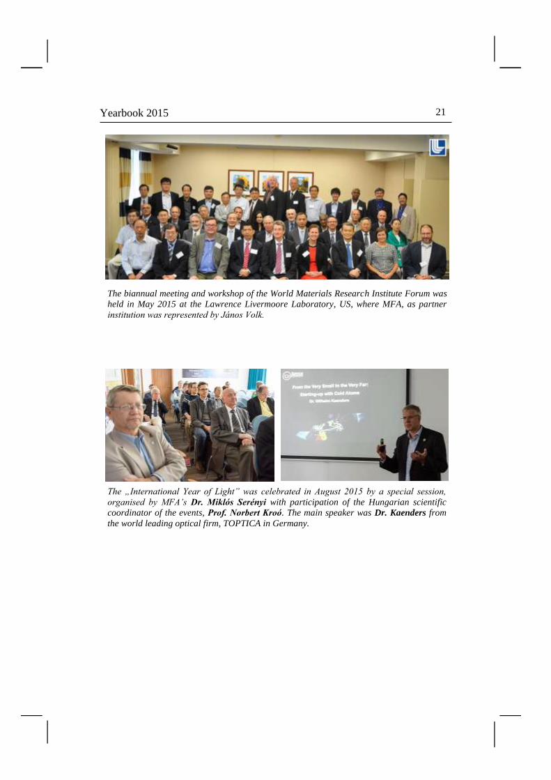
The biannual meeting and workshop of the World Materials Research Institute Forum was
held in May 2015 at the Lawrence Livermoore Laboratory, US, where MFA, as partner
institution was represented by János Volk.
The „International Year of Light” was celebrated in August 2015 by a special session,
organised by MFA’s Dr. Miklós Serényi with participation of the Hungarian scientific
coordinator of the events, Prof. Norbert Kroó. The main speaker was Dr. Kaenders from
the world leading optical firm, TOPTICA in Germany.

22
A scientific highlight of the year was the visit of Prof. Hiroshi Amano, Nagoya University,
one of the Nobel-Laureates for the development of the blue-LED. Prof. Amano, a real
modest and polite scientist delivered a nice talk on the progress of III-V nanodevices for a
very interested audience, and had a chat with top scientists of our institute on November 5
2015.

Yearbook 2015
23
In October a successful „International Workshopon on 2D materials” was organized by
the participants of the Korea-Hungary Joint Nanolaboratory, headed by Dr. Levente
Tapasztó and Prof. László P. Biró of MFA, and Dr. Chanyong Hwang (RISS, Korea).
In September 2015 in Freiburg, Germany, the
EUROSENSORS trophy was passed by the chair ofthe
EUROSENSORS 2015 conference, Prof. Gerald Urban
to the designated general chair of the next conference.
Prof. István Bársony is to organise the 30th
anniversary event in Budapest from September 4-7,
2016 under the auspices of the Engineering Chapter of
the Hungarian Academy of Sciences.

24
PUBLIC OUTREACH
The traditional MFA-Day was held in early June at splendid weather with about 180
guests all participating in cooking on open fire and enjoying sports, children’s joy and
each-other’s company with current and past colleagues and families.
Raising awareness for the activity of researcher in the natural science field was the event
“Researcher’s Night” in September 2015. The children are instructed by Dr. Orsolya
Tapasztó.

Yearbook 2015
25
The Summer School was organised for 23 high school children of age 16-17, selected
from the Hungarian schools of the Carpathian basin. Next to research also a program for
spending their free time by sports, sight-seeing and different other attractions were
compiled by Csaba S. Daróczi already the 8th time in 2015 in this traditional event.

26
Farewell party for Magdolna Erős (in the centre). Following four decades of excellent
laboratory-work in the clean-room of the Microtechnology Department she retired and
also obtained the Distinction of the Secretary General of the HAS.
We could not anticipate, that this will be the last occasion to meet Éva Vázsonyi (third
from left in the front row), who deceased end of March 2016.

Yearbook 2015
27
SCIENTIFIC REPORTS
Nanostructures Laboratory
Head: Prof. László Péter BIRÓ, corresp. member of the HAS
Research Staff
Zsolt Endre HORVÁTH, Ph.D., Deputy
Head of Laboratory
Prof. József GYULAI, Member of the
HAS (Professor Emeritus)
Antal Adolf KOÓS, Ph.D.
Géza István MÁRK, Ph.D.
Zoltán OSVÁTH, Ph.D.
Krisztián KERTÉSZ, Ph.D.
Péter NEMES-INCZE, Ph.D. (on leave)
Enikő HORVÁTH, Ph.D. (on leave)
Gergely DOBRIK, Ph.D.
Ph.D. students / Diploma workers
Péter Lajos NEUMANN, Ph.D.
student (on leave/left)
Gábor PISZTER, Ph.D. student
András PÁLINKÁS, Ph.D. student
Zsófia JUHÁSZ, diploma worker
2D Nanoelectronics „Lendület” Research Group
Group Leader
Levente TAPASZTÓ, Ph.D. (Head of the Nanostructures Lab since
1st December 2015)
Ph.D. students / Diploma workers
Péter VANCSÓ, Ph.D. student
Gábor MAGDA, Ph.D. student
Péter KUN, Ph.D. student
János PETŐ, diploma worker
The Nanostructures Laboratory has an almost two decade expertise in the production
and characterization of various nanostructures. Recently in the focus of our work
were various 2D nanostructures (graphene, h-BN, few-layer graphite and TMDCs),
their nanoarchitectures, bioinspired photonic nanoarchitectures and applications of
these nano-objects in various fields of nanotechnology, nanoelectronics and sensorics.
A novel cleaving procedure was developed, which allows production and atomic
scale characterization by STM/STS of large area TMDCs flakes.
Moire type superstuctures were investigated in detail which appear between CVD
graphene and HOPG for the full range of misorientation angles from 0 to 30.
Hybrids of CVD graphene and Au nanoparticles were produced and revealed was
SERS effect of significant magnitude.
Structural color of two Lycaenid butterfly species were detected and shown were
the consequently different prezygotic mating strategies, which exhibit similar
scatter around the mean value, but the average intensity of the coloration is related
with the mating strategy.
For more details, please feel free to visit the web page of the Nanostructures
Laboratory: (http://www.nanotechnology.hu/)

28
Exfoliation of large-area transition metal chalcogenide single
layers
(Lendület2014-14, KHJLN,OTKA-K 10875, OTKA 101599)
G. Z. Magda, J. Pető, G. Dobrik, C. Hwang (KRISS), L. P. Biró, and L. Tapasztó
Layered transition metal chalcogenides (TMCs) display strong intra-layer metal-
chalcogenide bonds, and a weak inter-layer bonding between neighboring planes of
chalcogenide atoms. The recent interest in studying their two-dimensional (2D) form
(consisting of triple to quintuple atomic sheets) is driven by the fact that the
properties of atomically thin crystals can drastically differ from their well-
characterized bulk counterparts. An eloquent example is the transition in the MoS2
band structure from indirect to direct band gap as the number of layers is reduced
from bulk to a single layer, opening the way towards optoelectronic applications.
Furthermore, the family of transition metal chalcogenides is large, covering a broad
range of properties from semiconductors (MoS2, WSe2) to semimetals (TiS2, TiSe2),
from topological insulators (Bi2Te3, Bi2Se3) to correlated materials (NbS2, NbSe2).
Such large variety of properties holds a huge potential for both fundamental studies
and applications, even graphene cannot compete with in spite of the unique versatility
of its properties.
The easy access to large TMC single layers is of key importance for exploring their
properties, in a similar manner as the facile isolation of large and high-quality
graphene flakes enabled the outstanding pace of the graphene research. As several
bulk TMC crystals are layered materials, similar to graphite, individual TMC layers
can be isolated by mechanical exfoliation (“scotch-tape” technique). Compared to
other methods, mechanical exfoliation provides 2D TMC sheets of high structural
quality enabling the fundamental study of their pristine properties, and ultimate
device performance, similar to graphene, where most of the fundamental discoveries
have been achieved on exfoliated samples, owing to their superior structural and
electronic quality. The major limitation of the micromechanical exfoliation of various
TMC materials is the small yield of single layers and their relatively small lateral size,
typically of a few microns, rendering the subsequent investigations and device
fabrication more difficult. This lateral size is about an order of magnitude smaller
than that of graphene flakes which can routinely be obtained by the same technique.
The reason for this probably originates from the unique mechanical strength and
ultra-strong adhesion of graphene to SiO2 that cannot be matched by the otherwise
still excellent mechanical properties of TMCs.
We have developed a novel mechanical exfoliation technique that overcomes the
limitations of the scotch-tape technique enabling the exfoliation of TMC single layers
with lateral size in the range of hundreds of microns. During the mechanical
exfoliation process, isolation of single layers is possible because the adhesion of the
bottom layer to the substrate becomes stronger than the adhesion to its own bulk
crystal. First, thick multilayer flakes had been peeled off from a bulk MoS2 crystal
using a thermal release tape, and these flakes had been placed on the top of the freshly

Yearbook 2015
29
cleaved gold substrates. We used a short ultrasonic treatment in acetone to remove the
thick MoS2 flakes from the gold surface. We found that after a few seconds of
sonication several thick flakes have been detached; however, underneath them, the
last (bottom) MoS2 layer remained attached to the gold substrate.
Figure 1 (a) Optical microscopy image of MoS2 single layer areas (1L, outlined by dotted
lines) with several hundreds of microns lateral size exfoliated on gold (Au 111) substrate.
(b) STM image of a MoS2 single layer exfoliated onto a gold substrate. The line cut
displayed was taken along the direction marked by the green line across the edge. (c)
Atomic resolution STM image of a MoS2 single layer revealing a hexagonal lattice
corresponding to the crystal lattice of the top sulfur atoms.
In optical microscopy images the MoS2 single layers can be identified as the areas of
the faintest color contrast as shown in Fig. 1. The optical images revealed several
hundreds of micron large areas covered by thin MoS2 layers. To confirm that these
areas of faintest optical contrast are indeed single layers of MoS2 we have performed
confocal Raman spectroscopy measurements. These measurements were indicating
that the several hundreds of microns large areas observed by optical microscopy can
be identified as MoS2 single layers. The exfoliated large flakes on top of the
conductive Au substrate enabled us to perform Scanning Tunneling Microscopy
(STM) measurements on mechanically exfoliated single layer MoS2 flakes. The
height of the investigated layers relative to the Au substrate was found to be about
0.7nm from the STM measurements (Fig. 1b), confirming the single layer thickness
of the exfoliated flakes. Atomic resolution images could routinely be achieved even
under ambient conditions (Fig. 1c). A hexagonal atomic lattice was revealed with a
3.1Å periodicity, corresponding to the lattice constant of the top layer of sulfur atoms.
We have also investigated whether the exfoliation process is specific to MoS2 or can
be applied more generally to various layered materials. We found that our exfoliation
method yielding large-area MoS2 flakes is not specific to molybdenum disulfide or
even sulfides, but works equally well for various layered chalcogenides, including
selenides and tellurides. Furthermore, in contrast to the standard scotch-tape method,
the exfoliation technique reported here is in principle able to achieve high coverage
rates of macroscopic substrates with various TMC single layers [78].

30
Structure and properties of graphene on gold nanoparticles
(EU FP7 Marie Curie CIG No.334377, OTKA-K101599, OTKA-PD-105173)
Z. Osváth, A. Deák, K. Kertész, Gy. Molnár, G. Vértesy, D. Zámbó, C. Hwang (KRISS, Korea), and L. P. Biró
Graphene covered metal nanoparticles constitute a novel type of hybrid materials,
which provide a unique platform to study plasmonic effects, surface-enhanced Raman
scattering (SERS), and metal-graphene interactions at the nanoscale. Such a hybrid
material is fabricated by transferring graphene grown by chemical vapor deposition
onto closely spaced gold nanoparticles produced on a silica wafer. The morphology
and physical properties of nanoparticle-supported graphene is investigated by atomic
force microscopy (AFM), optical reflectance spectroscopy, scanning tunneling
microscopy and spectroscopy (STM/STS), and confocal Raman spectroscopy.
Gold nanoparticles were prepared by evaporating a thin gold film of 5 nm onto a 285-
nm-SiO2/Si substrate at room temperature. Subsequent annealing was performed at
400 oC in Ar atmosphere for 30 minutes, which resulted in the formation of Au
nanoparticles with heights of 15-20 nm and high surface coverage. We transferred
graphene grown by chemical vapour deposition (CVD) onto the prepared gold
nanoparticles using thermal release tape. Fig. 1a shows a typical AFM image of the
transferred graphene which is considerably rippled. Note, that the lower part of the
image is not covered with graphene.
Figure 1 Tapping mode AFM image of graphene transferred onto Au nanoparticles. The
area marked by white square in (a) is presented with higher magnification in (b). The
black dot in (b) points out star-shaped rippling centred on the top of the underlying
nanoparticle. The height profiles representing the sections 1 and 2 are displayed in (c).
During the transfer with thermal release tape, the initial large area graphene breaks
into smaller sheets with dimensions of several micrometers and not all of them remain
attached to the nanoparticles. Fig. 1b is a higher magnification image which
corresponds to the white square drawn in Fig. 1a. The height profiles corresponding
to the line section 1 and 2 are displayed in Fig. 1c. Line section no. 1 is measured in
the area without graphene, showing a typical gold nanoparticle on the SiO2 surface,
with height of 18 nm. On the graphene-covered side, the line section no. 2 displays
the wavy shape of the graphene. The peaks in the height profile correspond to

Yearbook 2015
31
graphene directly supported by nanoparticles, whereas the dip corresponds to
graphene bridging two nanoparticles. Comparing the height profiles of line sections
1 and 2, we find that the graphene part bridging the nanoparticles is located more than
10 nm above the SiO2 substrate, i.e. it is suspended. In fact, this is a general
observation for the transferred graphene: it is suspended between gold nanoparticles.
We investigated the SERS activity of the graphene/gold nanoparticle sample by
confocal Raman spectroscopy performed both before and after annealing. Fig. 2a
show typical Raman spectra obtained with 488 nm laser on transferred CVD-grown
graphene without annealing. Note that there is no significant difference between
graphene peak intensities when measured on SiO2 and on gold nanoparticles,
respectively. In contrast, when using the 633 nm laser we observe an almost tenfold
enhancement (Fig. 2b) for the graphene G peak (1585 cm-1), as well as 4-fold
enhancement for the 2D peak. After annealing at 500 oC, these enhancement factors
increase to 13 and 22 for the G and the 2D peak, respectively (Fig. 2d). Furthermore,
nearly 6-fold peak enhancement is observed with the 488 nm laser also, but only for
the 2D peak (Fig. 2c). The higher enhancement at 633 nm laser is due to the fact that
this wavelength is closer to the localized surface plasmon resonance of gold
nanoparticles (597 nm), where the local electric fields are much more increased
compared to the off-resonance at 488 nm [96].
Figure 2 Raman spectra of graphene transferred onto gold nanoparticles (black line),
and of graphene transferred directly onto SiO2 substrate (red line). All spectra are
averaged over areas of 55 µm2 and normalized to the 2D peak height measured on
SiO2.

32
Electronic properties of MoS2 flakes grown on graphite
(János Bolyai Research Scholarship, OTKA K101599, Lendület2014-14, EU
REA 334377)
A. A. Koós, P. Vancsó, G. Z. Magda, Z. Osváth, K. Kertész, L. Tapasztó, C. Hwang, and L. P. Biró
Hybrids of 2D materials are expected to become building blocks of next generation
high performance nanoelectronic devices, like transistors and sensors. In addition to
graphene with zero-gap character, other 2D materials, such as MoS2 with a direct
band gap of 1.9 eV, are really interesting. These materials can complement each other
in 2D van der Waals heterostructures, offer a tool to engineer wide range of physical
properties and open new possibilities for applications. In order to understand the
properties of graphene - MoS2 hybrids, MoS2 sheets were grown by chemical vapour
deposition (CVD) on highly ordered pyrolytic graphite (HOPG). The heterostructures
were investigated with Scanning Tunneling Microscopy (STM) and Current Imaging
Tunneling Spectroscopy (CITS).
The MoS2 flakes were triangular (Fig. 1a) and followed the crystallographic
orientation of HOPG substrate. The high resolution STM image (Fig. 1b) shows two
overlapped periodic structures which form moiré pattern. The smaller 3.16 Å period
corresponds to the inter-atomic spacing of S atoms in MoS2, while the longer 12.5 Å
period was caused by the interaction between MoS2 and HOPG. The 12.5 Å period is
nearly 5 times the atomic distance in HOPG, and 4 times in MoS2, respectively.
Figure 1 a) STM image of a single layer MoS2 flake grown on HOPG (200 pA, 1.5 V).
b) Atomic resolution STM image of the flake exhibiting moiré type pattern (1 nA, 100 mV).
The inset shows a ball and stick model of sulphur (yellow) and carbon (grey) atoms.
The electronic properties of MoS2 flakes grown on HOPG were investigated using
CITS (Fig. 2). In CITS operation the scanning is interrupted in each image pixel, a
full I-V curve is recorded and the CITS map displays the tunneling current measured
at a selected bias voltage. The measured quasiparticle band gap for single-layer (SL)
MoS2 is around 2 eV, which decreases to 1.75 eV for bi-layer (BL) MoS2, in good
agreement with previous calculations and recent STM studies. The tunneling current
of MoS2 edges is different along the entire edge – irrespectively if the edge is located

Yearbook 2015
33
on HOPG (SL edge) or on MoS2 (BL edge) - from the current measured on flakes.
These changes appear more pronounced at negative voltages. The difference is also
clearly visible in the dI/dV spectra (Fig. 2d), where the MoS2 edges show a metallic
behaviour. Our STM measurements have confirmed that the edges of insulating MoS2
can be viewed as a one-dimensional metallic wire.
Figure 2 STM image (a), CITS maps (b, c) and dI/dV spectra (d) recorded on SL and BL
MoS2 flakes grown on HOPG.
STM nanolithography was used to cut MoS2 nanoribbons suitable for nanoelectronic
devices. The most accurate lines were cut when the cutting was started at the edge of
the MoS2 flake and performed in air with 90% relative humidity. With this method we
were able to cut less than 20 nm wide MoS2 nanoribbons for the first time (Fig. 3).
Figure 3 MoS2 nanoribbons cut by STM nanolithography on HOPG. a) ~15 nm and
b) ~12 nm wide MoS2 ribbons.

34
Atomic and electronic structure of native point defects in MoS2
single layers revealed by Scanning Tunneling Microscopy
(Lendület2014-14, KHJLN, OTKA 101599, OTKA 108753)
P.Vancsó, G. Zs. Magda, J. Pető, J.Y. Noh (KRISS, Korea), Yong-Sung Kim (KRISS, Korea), C. Hwang (KRISS, Korea), L. P. Biró, and L.Tapasztó
Transition metal dichalcogenide (TMDC) single layers have recently emerged as
strong competitors of graphene in electronic and optoelectronic applications due to
their intrinsic direct bandgap. However, atomic resolution TEM and electrical
transport measurements indicate the presence of a high concentration of intrinsic
structural defects. In this work we revealed the structure of native defects at truly
atomic scale by STM investigation of large area exfoliated MoS2 single layers, and
we provide information on their electronic properties by ab-initio calculations, too.
Fig. 1 shows typical atomic resolution STM images of 20 nm x 20 nm areas of a
MoS2 single-layer. The basic pattern observed is a hexagonal lattice of 0.31 nm
periodicity, corresponding to the atomic lattice of the top sulfur layer of the 2D MoS2
crystal. Line profiles (inset of Fig. 1b) across the dark triangles reveal that they are
centered on a lattice site of the top S layer, except that no S atom is present, indicating
their origin from a S vacancy. Since during the STM investigation the introduction of
novel point defects has never been observed, we can directly estimate their intrinsic
concentration in high quality exfoliated MoS2 single layers which is in the range of
1013-1014 cm-2.
Besides the frequently observed triangular defects in STM images (Fig. 2a), defects
of circular symmetry (Fig. 2b) have also been observed. To clarify the origin of the
point defects we have performed DFT calculations.
Figure 1 Atomic resolution STM images of native point defects in MoS2 single layers. A
high concentration (1013-1014 cm-2) of native point defects (dark triangles) has been
revealed by truly atomic resolution STM investigation of mechanically exfoliated MoS2
single layers on Au (111). The point defects (dark triangles) are centered on an empty site
of the hexagonal S atom lattice (see inset).

Yearbook 2015
35
Our calculations revealed two midgap electronic states (Fig. 2e) localized on the S
atom vacancy. The simulated STM images from the calculated local density of states
of the neutral a1 and e states show triangular and circular form (Fig. 2c,d), pointed
out that they are distinct STM images of the same structural defect.
By combining STM measurements with theoretical calculations our results provide
insight into the electronic structure of the native defects of MoS2 single layers, which
is of key importance for understanding the operation of realistic electronic devices
based on 2D crystals of molybdenum disulfide.
Figure 2 (a)-(b) Atomic resolution STM images of single-layer MoS2 with triangular and
circular shaped point defects at different spatial locations of the same flake. (c)-(d)
Simulated STM images of the two electronic mid-gap states of a S atom vacancy based on
DFT calculations. The sulfur and molybdenum atoms are shown by yellow and purple
circles, respectively. (e) Local density-of-states for a neutral sulfur atom vacancy with
midgap states.

36
Modulation of physical properties by stacking of 2D materials
(Lendület2014-14, KHJLN, OTKA 101599, OTKA 108753)
G. Dobrik, P. Vancsó, G. I. Márk, L. Tapasztó, Ph. Lambin (UNamur, Belgium), C. Hwang (KRISS, Korea), and L. P. Biró
The extraordinary properties of graphene induced a continuously increasing attention
focusing more recently on other 2D materials, too, like for example h-BN and the
transition metal dichalcogenides. These 2D layers offer the possibility of building
new materials, by stacking in a controlled way atomic/molecular thin layers in a layer
by layer sequence, leading to novel properties. The vertically stacked heterostructures
of 2D materials open a very wide range of possibilities the exploration of which may
offer solution from cheap gene sequencing to high temperature superconductivity. As
already demonstrated experimentally, the stacking each over the other of the 2D
atomic, or molecular crystals gives birth to a full range of very complex phenomena,
like Hofstadter’s Butterfly, new optical phenomena, charge density waves etc. These
may arise from several sources, for example: the lattice mismatch of the adjacent
layers; the chemical composition of the individual layers; the orientation of the
crystalline lattices of the adjacent layers. Therefore the investigation of the effects of
the above parameters may prove to be of paramount importance in understanding the
properties of the new material heterostructures systems.
Figure 1 Moiré structures at different angles of rotation (misorientation angles are given
in the upper right corners). The rotation angles accurately determined relative to the
HOPG substrate. Top left corner inserts; increased contrast..
In this work, we propose as a particularly suitable model system for the understanding
of vertically stacked 2D materials the CVD graphene on highly oriented pyrolytic
graphite (HOPG). A major advantage of this system is that it allows the separation of
chemical composition and lattice mismatch effects from lattice rotation effects. The
grain misorientation angles ranging from a few degrees to 30 degrees include the
entire range of interest. The moiré type superstructures appearing between the CVD
graphene layer and bulk HOPG (Fig. 1) was investigated by scanning tunneling
microscopy (STM), scanning tunneling spectroscopy (STS) and Raman spectroscopy.
We found that the different rotation angles caused various effects. At small rotation
angles <2° STS measurements show localized states at the Fermi energy (Fig. 2a).
When the rotation angle is increased, (between 2° and 7°) the STS measurements
reveal an interesting phenomenon, namely secondary Dirac cones are observed in the

Yearbook 2015
37
spectra (Fig. 2b). We found that the energy position of the 2nd Dirac cone is tunable
by the rotation angle following linear dependence. This peculiar band structure leads
to profound changes in the electronic transport measurement by increased resistivity.
Figure 2 STS spectra at small rotation angles. (a.) Localized states at the Fermi energy.
Inset:STM image with the measured points. (b.) Secondary Dirac cone as a function of the
angle of rotation.
Further increase of the rotation angle (above 15°) the 2D peak of graphene appears
near the graphite's 2D peak in the Raman measurements (Fig. 3). This suggests that
the graphene layer is vibrationally decoupled from the substrate. The STS spectra also
support the decoupling because no significant changes of the electronic properties
have been observed compared with the single layer graphene.
Figure 3 Raman shift of the rotated CVD graphene layer on HOPG. The graphene layer
is vibrationally decoupled from the substrate above 15° rotation angle.

38
Variability of structural coloration in blue butterfly wings
(OTKA K 111741)
K. Kertész, G. Piszter, Zs. Bálint (HNHM, Hungary), and L. P. Biró
Variation exists within all populations of living organisms. This is the basis of natural
selection where individuals that differ in phenotypes have different survival and
reproduction chances: individuals with the appropriate trait may survive and
reproduce more successfully than individuals with other, less suitable attributes, thus
the population is able to evolve. The reproductive success can be determined by
sexual selection, too, where one gender chooses mate based on phenotypic traits. The
conspicuous structural colour on the wings of Blue butterfly males constitutes an
important sexual communication channel; therefore it is subjected to strong
evolutionary pressure as individuals with the “wrong” colour have a lesser chance to
transmit their genes to the offspring.
Figure 1 Photograph images of male Blue butterflies: (a) P. icarus and (b) P. argus
specimens are shown. (c) Species-specific reflectance spectra of P. argus and P. icarus.
Note the wavelength difference of the main reflectance peak and the shoulder at 320 nm.
The structural colour of the wings is generated by photonic crystal type
nanoarchitecture which is located in the volume of the wing scales. This photonic
nanocomposite is constituted of spatially periodic chitin matrix with embedded air
holes with the characteristic size range of a few hundred nanometres. This
characteristic length of the components’ periodicity and the refractive index contrast
between them result in wavelength selective reflection in the blue which is the source
of the vivid structural coloration.
Structural colours of butterfly wings are more and more in the focus of attention both
from the point of view of physics, and biology. However, studies focusing on the
biologic variability of the structural coloration are mostly lacking. Therefore, we
investigated this variability of structural coloration in the case of two common
Lycaenid species living in Hungary. These species use their blue coloration for

Yearbook 2015
39
conspecific recognition, but display differences in prezygotic strategy as male
individuals of Polyommatus icarus (Fig. 1a) are patrolling, whilst Plebejus argus
(Fig. 1b) are lacking in their habitats. From both species 25 male individuals were
captured and the colour of all four wings was characterized spectrally, thus providing
100 measurements for each species.
Figure 2 (a) Histograms of amplitude and spectral position deviations of P. icarus and P.
argus males. (b) Averaged reflectance spectra of P. icarus and P. argus males. Significant
difference in the measured intensity can be seen.
The reflectance spectra of the wings were measured using normal incident white light
illumination and integrating sphere light collecting. The averaged reflectance spectra
of the two species were generated and normalized to the main reflectance peaks in the
blue to facilitate comparison. In Fig. 1c the species-specific colour differences of the
two species can be observed: there is a small (~15 nm) difference between the
wavelength of the maxima in the blue and the averaged spectrum of P. argus males
has an additional shoulder at 320 nm compared to P. icarus.
Based on these averaged spectra the averaged parameters (peak position, amplitude)
were determined for both species and the deviation of the two quantities were
calculated and histograms were generated (Fig. 2a). For the two investigated species
the intensity and wavelength deviations were almost identical which show that the
natural variability of the structural colour in the case of species living in the same
habitat is very similar due to the colour-based conspecific recognition.
To analyse the intensity of the blue structural colour the 100-100 measured
reflectance spectra were averaged by species without normalization and were plot
(Fig. 2b). The two averaged curves reveal the reflected intensity differences: the P.
icarus males show enhanced reflectivity in the visible wavelength range compared to
P. argus males resulting in brighter blue colour of the wings. This is in accordance
with the naked eye observations and can be a direct consequence of the different
prezygotic mating strategies of the two species while it requires different optical
properties: the patrolling males of P. icarus have to be more conspicuous for an easy
recognition by their females, but the perching mating strategy of P. argus males
lacking in their microhabitats requires less intense blue colour as the females have to
identify the males from significantly shorter distances.

40
Photonics Department
Head: Miklós FRIED, D.Sc., Scientific Advisor
Research Staff
Emil AGÓCS, Ph.D. (on leave)
Antal GASPARICS, Ph.D.
András HÁMORI, dr. univ.
Csaba S. DARÓCZI, dr. univ.
György JUHÁSZ, dr. univ.
György KÁDÁR, D.Sc.
Péter KOZMA, Ph.D. (-)
Csaba MAJOR, Ph.D. (-)
János MAKAI, C.Sc. (part time)
Norbert NAGY, Ph.D.
Olivér POLGÁR, Ph.D.(-)
Ferenc RIESZ, C.Sc.
Tivadar LOHNER, D.Sc.
Miklós SERÉNYI, D.Sc.
Gábor VÉRTESY, D.Sc.
Ph.D. students / Diploma workers
Bálint FODOR, Ph.D. student (on
leave)
Eszter FÜLÖP, Ph.D. (-)
Judit NÁDOR (1/2), Ph.D. student
Szilárd POTHORSZKY, Ph.D. student
Dániel ZÁMBÓ, Ph.D. student
MFA was involved in the UNION (EU FP7) (Ultra-versatile Nanoparticle Integration
into Organized Nanoclusters) project with the aim to develop tailored assembly of
nanoparticles to be used in the field of theranostics, thermoelectrics and lighting
applications. Main parameters investigated are the size of the template particles,
wettability of the substrate, and the drying kinetics (temperature). Due to the
arrangement of the gold nanoparticles, electromagnetic hot-spots can be created, that
can be exploited in different spectroscopy techniques. With proper surface chemistry
design, the ring-like structures can be also used to “focus” liquid dissolved molecules
to accumulate at the hot-spots upon solvent drying.
Mesoporous silica thin films were patterned at the sub-micron scale utilizing the ion
hammering effect in order to combine the advantages of mesoporous character and
surface morphology, while preserving the interconnected pore system or creating
laterally separated porous volumes surrounded by non-permeable compact zones.
Measurements confirmed that the majority of the porous volume can be preserved as
interconnected pore system by the application of low ion fluence. By increasing the
fluence value, however, separated porous volumes can be created at the expense of
the total pore volume.
Magnetic measurements are frequently used for characterization of changes in
ferromagnetic materials, because magnetization processes are closely related to their
microstructure. The recently developed method (Magnetic Adaptive Testing, MAT) is
based on the systematic measurement and evaluation of minor magnetic hysteresis
loops. This method was suggested as a highly promising non-destructive alternative

Yearbook 2015
41
of destructive tests for monitoring structural changes in ferromagnetic objects. MAT
introduces a large number of magnetic descriptors to diverse variations in non-
magnetic properties of ferromagnetic materials, from which those, optimally adapted
to the just investigated property and material, can be picked up. This year, satisfactory
correlation between nondestructively measured magnetic descriptors and actual
lifetime of the fatigued material were found. The method is able to serve as a
powerful tool for indication of changes, which occur in structure of the inspected
objects during their industrial service lifetime, as long as they are manufactured from
ferromagnetic materials.
We are involved in 2 EU-projects („SEA4KET” and the ENIAC-2012-2 “E450DL”)
to develop “Imaging Optical Inspection Device With A Pinhole Camera”. We
developed 30, 45-60 and 60-90 cm wide prototypes.
Finite element simulations were used to calculate optical response of rough surfaces.
This way, we can generate any surfaces for the investigation of the usually simplified
optical models of ellipsometry or for other characterization methods. In agreement
with previous investigations on polysilicon samples, correlation between the
thickness of the effective medium layer and the RMS roughness was found. Our
method also allows to investigate limits of the effective medium approach more in
details.
A special flow cell for plasmon-enhanced, internal reflection, multiple-angle of
incidence in situ spectroscopic ellipsometry was developed by MFA, which can be
used to monitor interface processes with a high sensitivity (~40 pg/mm2) and speed
(less than 1 s for a full spectrum) in a broad wavelength range (350-1690 nm). The
device was succesfully applied to study protein adsorption, cell adhesion and
polyelectrolyte deposition simultaneously on uncoated and titania nanoparticle-coated
gold surfaces.

42
Nondestructive indication of fatigue damage in ferromagnetic
construction materials
(OTKA K 111662)
G. Vértesy, Cs.S. Daróczi, and A. Gasparics
Magnetic measurements are frequently used for characterization of changes in
ferromagnetic materials, because magnetization processes are closely related to their
microstructure. The recently developed method (Magnetic Adaptive Testing, MAT) is
based on the systematic measurement and evaluation of minor magnetic hysteresis
loops. This method was suggested as a highly promising non-destructive alternative
of destructive tests for monitoring structural changes in ferromagnetic objects. MAT
introduces a large number of magnetic descriptors to diverse variations in non-
magnetic properties of ferromagnetic materials, from which those, optimally adapted
to the just investigated property and material, can be picked up.
Many ferromagnetic components are subjected to alternating load in service, which
often causes their structural failure as a result of fatigue. Fatigue evaluation and
residual lifetime assessment are challenging issues with a high profile in industry.
Nearly 90% of industrial component failures take place due to fatigue that occurs
without warning. In order to check up health of ferromagnetic construction materials,
it is important to timely monitor their fatigue damage, i.e. to detect initiation and
propagation of fatigue cracks, and to predict residual lifetime of the constructions.
Fatigue damage was investigated in cyclically loaded low-carbon steel, by the MAT
method. A sample made of cold-rolled S235JR steel was chosen for presentation of a
typical MAT-measurement of the fatigue damage process. The specimen is
ferromagnetic, it is flat, and it can be magnetized for the MAT-measurement by a
short solenoid placed over the critical volume, where the fatigue cracks are initiated
in the sample. This critical area is the neck, close to the fixed bottom head of the
sample. The MAT-measurement of the samples proceeded in such a way, that always
after a chosen number of loading cycles a short solenoid containing both the
magnetizing and the pick-up coils was placed over the critical part of the sample, a
couple of passive soft magnetic yokes was pressed to the sample so, that they and the
sample created a closed magnetic circuit, and one family of the minor permeability
loops was recorded. Then the yokes were taken away and a next number of loading
cycles were applied. Fig. 1 shows the sample with the yokes and with the yoke-holder
during the magnetic measurement.
Fig. 2 presents the result of the magnetic measurements. It is seen here, how the
properly chosen MAT descriptor changes due to the cyclic loading. The sample was
broken after 230 000 cycles. A very significant and fast increase of magnetic
parameters close the end of the sample’s lifetime is observed.
As a conclusion, satisfactory correlation between nondestructively measured
magnetic descriptors and actual lifetime of the fatigued material were found. The
method is able to serve as a powerful tool for indication of changes, which occur in

Yearbook 2015
43
structure of the inspected objects during their industrial service lifetime, as long as
they are manufactured from ferromagnetic materials.
Figure 1 The critical part of the
sample is covered by the
magnetizing/sensing solenoid and
by a couple of passive soft yokes
pressed to the surface of the
sample with a plastic spring
holder. All are fixed at the bottom
in a vice with non-magnetic jaws.
The couple of deflection
electromagnets can be seen at top
of the figure.
Figure 2 The optimally chosen
MAT descriptor as a function of
cyclic loading. The fast upward
curvature after 200 000 cycles
indicates start of the critical crack
spreading through the sample.

44
Makyoh topography
F. Riesz, and J.P. Makai
In collaboration with IMEM–CNR, Parma, the surface shape and morphology of hot-
wall VPE grown SiC/Si heterostructures have been characterized with Makyoh
topography in order to study the effects of the addition of methyl trichloro silane.
Low amount of sample bow was obtained in an optimized growth process. Fig. 1
shows a characteristic topogram, showing interference fringes related to thickness
inhomogeneity and edge slip lines.
Figure 1 Makyoh-topography image of a SiC/Si heterostructure.
Within the project KMR_12-1-2012-0226, in collaboration with Mirrotron, Ltd. and
the Wigner Research Centre for Physics, surface flatness of large-area polished Ni(P)
coated Al blocks were characterised for neutron guide applications. Fig. 2 shows the
purpose-built sample positioning/translation stage.
Figure 2 Sample positioning stage for Makyoh characterisation of large-areas samples.

Yearbook 2015
45
Determination of migration of ion-implanted Ar and Zn in
silica by backscattering spectrometry
(OTKA K101223)
I. Bányász, E. Szilágyi, E. Kótai, A. Németh, Cs. Major, M. Fried, and G. Battistig
It is well known, that refractive indices of materials important for waveguide
fabrication, can be modified by ion implantation. In this work, effect of Ar and Zn ion
implantation on silica layers was investigated by Rutherford Backscattering
Spectrometry (RBS) and Spectroscopic Ellipsometry (SE). Silica layers produced by
chemical vapour deposition technique on single crystal silicon wafers were implanted
by Ar and Zn ions. The refractive indices of the implanted silica layers before and
after annealing at 300 C and 600 C were determined by SE.
The migration of the implanted element was studied by real-time RBS up to 500 C.
It was found that the implanted Ar escapes from the sample at 300 C. Although the
refractive indices of the Ar implanted silica layers were increased compared to the as-
grown samples, but after annealing this increase in the refractive indices has
vanished. In case of the Zn implanted silica layer both the distribution of Zn and the
change in the refractive indices were found to be stable. Zn implantation seems to be
an ideal choice for producing waveguides.
Figure 1 Refractive indices for Ar implanted
samples. For comparison, the refractive
indices of virgin sample and the thermal SiO2
(from literature) are also shown.
Figure 2 Refractive indices as a function of
wavelength for the two sublayers in the Zn
implanted sample. For the sake of
comparison the refractive indices of the
virgin oxide as well as the thermal oxide are
also shown.

46
Verification of the effective medium approximation for surface
roughness by finite element method
(OTKA K115852, K81842)
B. Fodor, P. Kozma, S. Burger, M. Fried, and P. Petrik
Finite element simulations were used to calculate optical response of rough surfaces.
This way we can generate any surface for the investigation of the simplified optical
models of ellipsometry or other characterization method. In agreement with previous
investigations on polysilicon samples, we found a correlation between the thickness
of the effective medium layer and the RMS roughness. Our method also allows to
investigate limits of the effective medium approach in more detail (see Fig. 1 and Ref.
B. Fodor, P. Kozma, S. Burger, M. Fried, P. Petrik, “Effective medium approximation
of ellipsometric response from random surface roughness simulated by finite element
method”, accepted for publication in Thin Solid Films in 2016).
Figure 1 (top) Random surface
generated by the JCMWave finite
element method.
(bottom) Correlation between the
product of RMS roughness and
RMS slope (RRMS*Rdq) and the
thickness of the effective medium
roughness (dEMA) with linear fit
for abscissa values smaller than
2 nm. The inset shows the
secondary effect of correlation
length (ξ) on dEMA for points
which have an RRMS*Rdq value of
~3.4 nm.

Yearbook 2015
47
Plasmon-enhanced two-channel Kretschmann ellipsometry
(OTKA K115852, M-ERA.NET “WaterSafe”)
J. Nádor, B. Kalas, E. Agócs, A. Saftics, P. Kozma, L. Kőrösi, I. Székács, M. Fried, R. Horváth, and P. Petrik
We have developed a flow cell in semi-cylindrical Kretschmann configuration for
plasmon-enhanced, internal reflection, multiple-angle of incidence in situ
spectroscopic ellipsometry, which can be used to monitor interface processes with a
high sensitivity (~40 pg/mm2) and speed (less than 1 s for a full spectrum) in a broad
wavelength range (350-1690 nm) (see Fig. 1, [109]; and [J. Nádor, B. Kalas, A.
Saftics, E. Agócs, P. Kozma, L. Kőrösi, I. Székács, M. Fried, R. Horváth, and P.
Petrik, “Plasmon-enhanced two-channel in situ Kretschmann ellipsometry of protein
adsorption, cellular adhesion and polyelectrolyte deposition on titania
nanostructures”, submitted for publication]. The cell has a small volume (10 l), and
it can readily be used with conventional table-top ellipsometers. Configuration with
the semi-cylinder allows multi-channel measurements when moving the cell parallel
to the axis of the cylinder using a conventional mapping stage.
The device was successfully applied to study protein adsorption, cell adhesion and
polyelectrolyte deposition simultaneously on uncoated and titanium nanoparticle-
coated gold surfaces.
Figure 1 (a): Flow cell with a semi-cylindrical lens in the Kretschmann configuration with a
gold-covered glass substrate. inset: The 10 µl flow–cell surrounded by an O-ring.
(b): A schematic graph of the measurement geometry.

48
Protein adsorption, cell adhesion and polyelectrolyte deposition
on titania nanoparticle coatings studied by two-channel
Kretschmann ellipsometry
("Lendület" grant LP2012-26/2012 of HAS, OTKA K115852, M-ERA.NET
“WaterSafe”)
J. Nádor, B. Kalas, E. Agócs, A. Saftics, P. Kozma, L. Kőrösi, I. Székács, M. Fried, R. Horváth, and P. Petrik
A flow cell in a semi-cylindrical Kretschmann configuration for performing in situ
two-channel measurements with a high sensitivity (~40 pg/mm2) was developed. A
setup was applied allowing to carry out simultaneous measurements on titania
nanoparticle (TNP) coated and uncoated gold surfaces, in order to reveal the effects
of the coating on protein adsorption, cell adhesion and polyelectrolyte layer
deposition [J. Nádor, B. Kalas, A. Saftics, E. Agócs, P. Kozma, L. Kőrösi, I. Székács,
M. Fried, R. Horváth, and P. Petrik, “Plasmon-enhanced two-channel in situ
Kretschmann ellipsometry of protein adsorption, cellular adhesion and polyelectrolyte
deposition on titania nanostructures”, submitted for publication]. One of the main
advantages of this approach is that the measurements on the two different surfaces are
performed in the same process, under same conditions (temperature, pH,
concentration etc.). Therefore, comparison of the two kind of measurement is more
reliable than before, because most of the systematic errors can be ruled out, and
concerns about repeatability are minimized.
Figure 1 The typical curves of a represen-
tative in situ ellipsometric measurement of
Fgn adsorption on TNP-coated and uncoated
surfaces.
Figure 2 The adsorbed mass density and the
thickness of the deposited 10 pairs of
PSS/PAH layers at pH 8 on TNP-coated and
uncoated gold surfaces
In the protein adsorption experiments a stable and widely used protein, fibrinogen
(Fgn) was investigated. Kinetic curves showed that adsorption of proteins was
enhanced on TiO2-coated surface (Fig. 1), which can be explained by the increased
specific surface area due to the TiO2 nanoparticles.
In the case of preosteoblast cell adhesion no proper ellipsometric model was found in
the evaluation, so the ellipsometric measurement proves only that the coating

Yearbook 2015
49
modifies the adhesion of the cells. After the measurement, images were taken with
phase-contrast microscope of the residual cells on the surfaces. On the TNP-coated
surface significantly more cells were observed, which reveals that the cells adhered
stronger to the coated surface.
For the process of polyelectrolyte layer-by-layer adsorption, poly(allylamine
hydrochloride) (PAH) and poly(styrene sulfonate) (PSS) was applied as positively
and negatively charged polyelectrolyte, respectively. Ten pairs of layers were built
and measured in real-time, at pH 8, where both the titania and the gold thin film has
negative charges on its surface. The thicknesses of the layers were demonstrated to be
increased by the TNP-coating (Fig. 2).
The measurement was also carried out at pH 4, where the surfaces are positively
charged. The thickness of the deposited layers was significantly larger at the basic pH
than at the acidic pH (Fig. 3). The difference between the thicknesses of the bilayers
at the acidic and basic pH can be explained by the strong pH-dependence of the
polyelectrolyte layer deposition.
Figure 3 The adsorbed mass density and the thickness of the deposited 10 pairs of
PSS/PAH layers on TNP coated surface at pH 8 and pH 4.

50
Development of optical metrology tool for in-line qualification
of thin films on large area
(EU FP7 SEA4KET, ENIAC E450EDL)
Cs. Major, Gy. Juhász, P. Petrik, and M. Fried
We are involved in 2 EU-projects („SEA4KET” and the ENIAC-2012-2 “E450DL”)
to develop “Imaging Optical Inspection Device With A Pinhole Camera”. We
developed 30, 45-60 and 60-90 cm wide prototypes (Figs 1, and 2).
Figure 1 We successfully installed our mapping device in the clean-room of IISB
(Erlangen, Germany). A 300 mm diameter wafer can be seen on the robotic arm (left side).
Figure 2 Thickness-map of a nominally 2000 nm thick oxide layer on a 300 mm diameter
Si-wafer (a) and the Meaned Squared Error-map showing the edges of the 30 cm diameter
wafer (b).

Yearbook 2015
51
Preparation of compact nanoparticle clusters from
polyethylene glycol-coated gold nanoparticles by fine-tuning
colloidal interactions
(OTKA K112114, PD105173 and FP7 No.310250 UNION)
D. Zámbó, Gy. Z. Radnóczi, and A. Deák
Control over colloidal interactions might allow the creation of nanoparticle
assemblies from individual, nanometric building blocks, giving rise to special optical
or optoelectronic properties. These assemblies are excellent candidates for some
advanced applications in the field of sensorics, energy harvesting, catalysis,
biomedical contrast agents, or even theranostics. Gold nanoparticles are exceptional
building blocks for nanoparticle assemblies as they support localized surface plasmon
resonances, which is very sensitive to the interparticle distance caused biplasmon
coupling. Polyethylene glycol homopolymers are commonly used as a stabilizer agent
of gold nanoparticles in various media.
Low-molecular weight polyethylene glycol (PEG) has a lower critical solution
temperature well outside the boiling point of water at ambient pressure, but it can be
reduced at high ionic strengths. We extend this concept to trigger the clustering of
gold nanoparticles through the control of colloidal interactions. At high ionic
strengths, low-molecular weight (<2000 Da) mPEG-SH-modified gold nanoparticles
show clustering with an increase in the solution temperature. The clustering
temperature decreases with an increasing ionic strength. The clustering is attributed to
the delicate interplay between the high ionic strength and elevated temperature and is
interpreted in terms of chain collapse of the surface-grafted PEG molecules.
Figure 1 Schematic representation of self-assembly of PEG-covered gold nanoparticles
into compact nanoparticle cluster.
The chain collapse results in a change in the steric interaction term, whereas the high
ionic strength eliminates the double-layer repulsion between the particles. The
observations are backed by nanoparticle interaction model calculations. We found
that the intermediate attractive potential on the order of a few kT allows the

52
experimental fabrication of compact nanoparticle clusters in agreement with
theoretical predictions.
A new approach for the predesigned, externally triggered clustering of gold
nanoparticles was also presented. On the basis of the calculations on the colloidal
interaction between the particles and the measurement data, it can be inferred that the
experimentally observed clustering of the nanoparticles at high ionic strength and
elevated temperature is a result of the chain collapse of the surface-grafted PEG
molecules. Threshold temperature of the clustering can be influenced by the ionic
strength of the medium. We found that the presence of the PEG shell significantly
influences the kinetics of the clustering. The deceleration of particle association can
be interpreted in terms of a moderate attractive potential after the chain collapse.
Figure 2 DLS size distribution of gold
nanoparticles as a function of temperature
for different salt concentration.
Figure 3 SEM images of compact
nanoparticle clusters from PEGylated
particels and fractal-like aggrates of citrate
stabilized nanoparticles.
The structure of the clusters agrees well with theoretical predictions for such a model
system. When the attractive potential between the building blocks is large, the
position of two attaching particles gets kinetically trapped and not allowed to
reconfigure during the assembly process, resulting in a fractal-like structure. This can
be observed for our control sample (Fig. 3c), where the elimination of the double-
layer forces leads to a rapid aggregation and fractal-like structure. For the PEG-
grafted nanoparticles, at moderate interparticle attraction, reconfiguration of the
building blocks is allowed; hence, the structure of the cluster becomes more compact.
The presented approach allows preparation of complex nanoparticle clusters, where
different type of nanoparticles can be incorporated into a single cluster [160].

Yearbook 2015
53
Introducing nanoscaled surface morphology and percolation
barrier network into mesoporous silica coatings
(OTKA K112114, PD105173 and FP7 No.310250)
E. Albert, P. Basa, A. Deák, A. Németh, Z. Osváth, G. Sáfrán, Z. Zolnai, Z. Hórvölgyi, and N. Nagy
Mesoporous silica thin films were patterned at sub-micron scale utilizing the ion
hammering effect in order to combine advantages of mesoporous character and
surface morphology, while preserving the interconnected pore system or creating
laterally separated porous volumes surrounded by non-permeable compact zones.
Thin coatings of mesoporous silica on Si substrate were prepared by sol-gel method
with ordered and disordered pore system using Pluronic PE 10300 and CTAB as
molecular templates. Hexagonally ordered Langmuir-Blodgett films of spherical
silica particles were transferred on the top of the porous silica coatings and applied as
mask against Xe+ ion irradiation (Fig. 1). The ion energy was chosen according to
Monte-Carlo simulations to achieve structures with high lateral contrast between
irradiated and unirradiated, i.e., masked areas.
Figure 1 Schematics of the key step of
sample preparation: ion irradiation with
200 keV Xe+ through an ordered monolayer
of silica spheres then removal of the
particles.
Figure 2 AFM images of Pluronic-type
silica coatings after ion irradiation with
fluences of (a) 0.1 × 1016 cm-2, and (b)
1 × 1016 cm-2, respectively. The measure-
ments were carried out (a) where the edge of
the particulate LB mask was located and (b)
at the border of irradiated and unirradiated
regions of the LB film.

54
The aspect ratio of resulted morphology was proved to be high; the created surface
structures were very similar irrespectively of the type of template molecules and ion
fluences applied (Fig. 2). The densification of both types of porous silica coatings
almost reached its maximum already at the lowest fluence. For CTAB-templated
coatings the degree of densification was significantly higher than in the Pluronic-
templated ones.
The HRTEM analysis revealed that the pore structure remained intact where the silica
spheres were non-transparent for the bombarding ions. For Pluronic-templated silica
samples with disordered pore system the pore structure remained interconnected near
the Si substrate surface at the lowest fluence. Contrarily, at the highest fluence, the
regions surrounding the intact porous columns were fully densified thus forming non-
porous border zones (Fig. 3). Therefore, the interconnected or the separated character
of the pore system can be tailored by the applied ion fluence, while the created
surface morphology is essentially the same in both cases. In case of CTAB-templated
coatings with ordered pore structure the results were similar. The densified regions
are thicker, while the intact porous volumes are smaller than in the Pluronic-
templated case irradiated with the same fluence. Comparing the two different
molecular templates the disordered Pluronic-templated pore system proved to be
more resistant against Xe-bombardment.
Figure 3 HRTEM images of (a) Pluronic-type and (b) CTAB-type coatings irradiated
with fluences of 0.1 × 1016 cm-2, and 1.0 × 1016 cm-2.
Confocal fluorescent images and ellipsometric porosimetry measurements confirmed
that the majority of the porous volume can be preserved as interconnected pore
system by the application of low ion fluence. By increasing the fluence value,
however, separated porous volumes can be created at the expense of the total pore
volume [3].

Yearbook 2015
55
Effect of heat treatments on the properties of hydrogenated
amorphous silicon for PV and PVT applications
(MTA 1102, OTKA K-67969, NF 101329, NK 105691, TAMOP 4.2.2.A-
11/1/KONV-2012-0036)
M. Serényi, N. Q. Khánh, and C. Frigeri
Photovoltaic (PV) solar cells and photovoltaic thermal (PVT) hybrid devices very
often employ hydrogenated a-Si (a-Si:H) because of its cost effectiveness and better
performance as light absorber. The properties of a-Si:H can be improved by heat
treatments that also help to recover the Staebler-Wronski effect. The effects of heat
treatments on the properties of hydrogenated a-Si to be used in PV and PVT devices
have been investigated. To better study them the annealing was performed at
temperatures (350 °C) higher than those (≈200-275 °C) usually applied to improve
the performance of a-Si:H employed in PV and PVT technologies since those effects
were expected to be stronger and more easily detectable. It was found that the heat
treatment causes changes in the Si-H bonding configuration with the transformation
of the SiH monohydrides to the less stable SiH2 dihydrides and polysilane chains. The
latter polyhydrides, in their turn, cause a strong degradation of the a-Si layer
morphology with the formation of surface blisters with size of some microns as well
as craters depending on the H content and annealing time.
Figure 1 Typical IR absorption spectra in the stretching mode range of the wavenumber
for the H content of a) 10.8, b) 14.7, c) 17.6 at%. For each plot the spectra for the
unannealed (solid curve), annealed for 1 h (dash curve) and for 4 h (dot curve) are
reported.

56
Microtechnology Department
Head: Gábor BATTISTIG, Ph.D., senior research fellow
Research Staff
Zsófia BAJI, Ph.D.
István BÁRSONY, Member of HAS
Gábor BATTISTIG, Ph.D.
László DÓZSA, Ph.D.
Csaba DÜCSŐ, Ph.D.
Zoltán FEKETE, Ph.D. (on leave)
Péter FÖLDESY, Ph.D.
Péter FÜRJES, Ph.D.
Zoltán HAJNAL, Ph.D.
Nguyen Quoc KHÁNH, Ph.D.
Zoltán LÁBADI, Ph.D.
István LUKÁCS, Ph.D.
György MOLNÁR, Ph.D.
Andrea Edit PAP, Ph.D. (part time)
Anita PONGRÁCZ, Ph.D.
Vilmos RAKOVICS, Ph.D.
István RÉTI, Ph.D.
Attila Lajos TÓTH, Ph.D. (retired)
János VOLK, Ph.D.
Zsolt ZOLNAI, Ph.D.
Ph.D. students
Zsófia BÉRCES
Zoltán SZABÓ
Ferenc BÍRÓ
Máté TAKÁCS
Róbert ERDÉLYI
Gergely MÁRTON
Tamás KÁRPÁTI
Eszter HOLCZER
Eszter TÓTH
Technical Staff
János FERENCZ (engineer)
Levente ILLÉS (engineer)
Csaba LÁZÁR (engineer)
Róbert HODOVÁN (engineer)
András LŐRINCZ (engineer)
Erika TUNYOGI (engineer, on leave)
Katalin VERESNÉ VÖRÖS
(engineer)
György ALTMANN (technician)
Gabriella BÍRÓ (technician)
Sándor CSARNAI (technician)
Tibor CSARNAI (technician)
Magda ERŐS (retired)
Károlyné PAJER (technician)
Csilla ARIAS-SOTONÉ FARAGÓ
(technician)
Attila NAGY (technician)
Magda VARGA (technician)

Yearbook 2015
57
The task of the Microtechnology Department is
Fundamental research on:
sensing principles;
novel materials and nanostructures;
novel 3D fabrication techniques.
Research and development of physical, chemical/biochemical sensors and
integrated systems:
MEMS – R&D on micropellistor-type gas sensors, 3D force sensors, thermal
sensors, CMOS compatible and related techniques.
BioMEMS – Development of novel microfluidic systems, their application in new
fields of biochemistry.
NeuroMEMS – Development of Si- and polymer based sensors for biomedical
applications with special focus on brain science.
NEMS – Synthesis and characterization of quasi-one-dimensional semiconducting
nanostrucrures, semiconductor nanodevices, their integration into functional
sensors, optoelectronic and photovoltaic devices.
Modelling, structural and device characterization methods available:
Electrical characterization;
Thermo-mechanical characterization;
Scanning Microprobes;
Ion beam analysis methods;
SEM, TEM, EDX;
Spectroscopic Ellipsometry.
The Department runs two (300 m2 + 160 m2) clean labs (Class 100-10000)
comprising a complete Si-CMOS processing line and a mask shop, unique facility in
Hungary. The technology allows to manufacture layers, patterned structures and
devices with line resolution of 1 µm by optical and down to 10 nm by e-beam
lithography on 3” and 4” Si and glass wafers.
Competences (available also for our industrial and academic partners and customers):
High temperature annealing, diffusion and oxidation;
Ion implantation;
Rapid Thermal Treatment;
Low Pressure Chemical Vapor Deposition of poly-Si, SiO2 and Si3N4 layers;
Low Temperature Chemical Vapor Deposition;
Atomic Layer Deposition;
Physical Vapor Deposition – Electron beam evaporation, DC and RF Sputtering;
Reactive Ion Etching, Deep Reactive Ion Etching;

58
Photolithography with back-side alignment and Nanoimprinting;
E-beam lithography;
Nanopatterning, deposition and etching by Focused Ion-Beam;
Wafer-bonding;
Wet chemical treatments;
Electro-chemical porous Si formation;
Molecular Beam Epitaxy of III-V compound semiconductors;
Mask design, laser pattern generator;
Polymer (PDMS, SU8, Polyimide) structuring by photolithography and micro-
molding techniques;
Chip dicing, packaging especially for sensor applications;
Materials and structural analysis & characterization: SEM, FIB, EDX, Atomic
Force Microscopy, Electrochemical Impedance Spectroscopy, Stylus Profiler;
Electrical and functional modeling and characterization.
For detailed information please visit our web-site: www.mems.hu
or contact us bye-mail: [email protected]

Yearbook 2015
59
MEMS
Activity leader: Cs. Dücső
Group members: Z. Baji, I. Bársony, G. Battistig, L. Dózsa, P. Földesy, P. Fürjes, Z.
Hajnal, Z. Lábadi, G. Molnár, A.E. Pap, V. Rakovics, I. Réti, A.L. Tóth, Z. Zolnai, F.
Biró, T. Kárpáti, M. Takács
Projects:
ENIAC CALL 2013-1 – “Intelligent Catheters in Advanced Systems for
Interventions – INCITE”
OTKA K109674 – “Graphen based terahertz modulators”
OTKA PD116579 – “ZnO és Ga2O3 nanostruktúrák készítése atomi
rétegleválasztással”
OTKA K112114 – “Kombinált mikro-nanotechnológiai eljárások és ellenőrzésük
lokális analitikai technikákkal: a mintázatképzéstől az alkalmazások felé”
KMR-12-1-2012-0107 – “Műszerfejlesztés talajvíz és egyéb vizek szénhidrogén
szennyezettségének folyamatos megfigyelésére”
KMR-12-1-2012-0226 – “Új generációs neutronos vizsgálóberendezések
komponenseinek fejlesztése (2012-2015)”
KMR_12-1-2012-0031 – “Beágyazott informatikai rendszer fejlesztése
energiapozitív közvilágítás optimálására”
Fine-tuning of gas sensitivity by modification of nano-
crystalline WO3 layer morphology
Hexagonal WO3 layers of different morphologies were deposited on micro-hotplate
gas sensors and gas sensitivity for NH3 was tested. The layers were synthesized by
hydrothermal acidic precipitation method using different catalytic chemicals. Thin
film sputtered layers were also deposited as reference material. WO3 suspensions of
quasi-equivalent quantity were dropped on the micro-hotplate for all the materials
investigated. Additional ultrasonic agitation was introduced to destroy conglomerates
of nano-crystals. If Na2SO4 or K2SO4 catalyst were added to the acidic solution of
Na2WO4, ultrasonic treatment proved to be very effective and resulted in uniform
sized individual WO3 nano-rods of 80nm diameter. Addition of ZnSO4 catalyst leads
to disordered nano-fiber net with typical diameter of 70 nm. Ultrasonic agitation had
no effect in case of NaCl catalyst and Zocher methods; thereby the formed WO3
layers are composed of micrometer size conglomerates of 80-150 nm nano-rods.
SO42- ions facilitate the formation of long crystallites.
Layers composed of individual nano-rods exhibit 2-5 times higher sensitivity up to
60ppm NH3, while layers of larger conglomerates show linear response in the
10-100ppm range. The size effect is explained by the comparable sizes of nano-wire

60
width and space charge layer at the solid-gas interface. This effect was also
demonstrated by the sputtered thin films of different thicknesses.
NaxWO3 contamination deteriorates gas sensitivity. No relationship between specific
surface and gas sensitivity could be detected.
Figure 1 SEM views of hydrothermally synthesised WO3 layers with different catalysts:
(A*): Na2SO4 without ultrasonic treatment, (A): Na2SO4 with ultrasonic treatment,
(B): K2SO4 with ultrasonic treatment, (C): NaCl with ultrasonic treatment, (D): ZnSO4
with ultrasonic treatment, (E): Zocher-method.
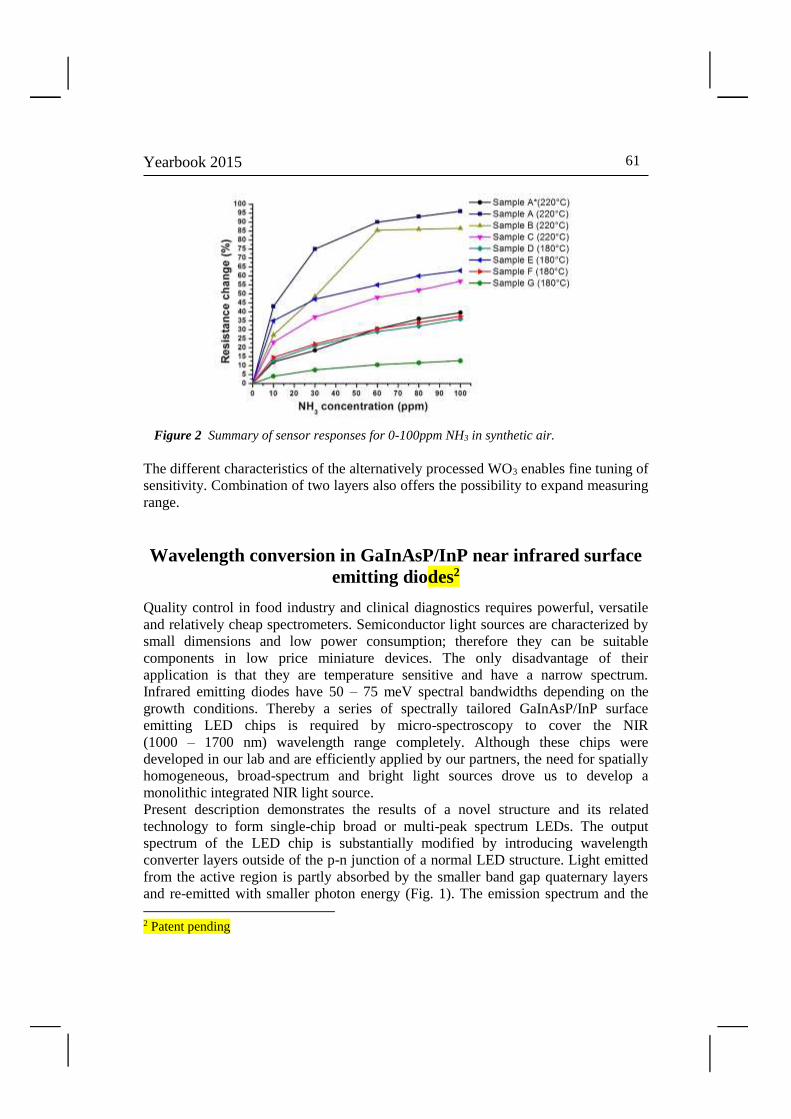
Yearbook 2015
61
Figure 2 Summary of sensor responses for 0-100ppm NH3 in synthetic air.
The different characteristics of the alternatively processed WO3 enables fine tuning of
sensitivity. Combination of two layers also offers the possibility to expand measuring
range.
Wavelength conversion in GaInAsP/InP near infrared surface
emitting diodes2
Quality control in food industry and clinical diagnostics requires powerful, versatile
and relatively cheap spectrometers. Semiconductor light sources are characterized by
small dimensions and low power consumption; therefore they can be suitable
components in low price miniature devices. The only disadvantage of their
application is that they are temperature sensitive and have a narrow spectrum.
Infrared emitting diodes have 50 – 75 meV spectral bandwidths depending on the
growth conditions. Thereby a series of spectrally tailored GaInAsP/InP surface
emitting LED chips is required by micro-spectroscopy to cover the NIR
(1000 – 1700 nm) wavelength range completely. Although these chips were
developed in our lab and are efficiently applied by our partners, the need for spatially
homogeneous, broad-spectrum and bright light sources drove us to develop a
monolithic integrated NIR light source.
Present description demonstrates the results of a novel structure and its related
technology to form single-chip broad or multi-peak spectrum LEDs. The output
spectrum of the LED chip is substantially modified by introducing wavelength
converter layers outside of the p-n junction of a normal LED structure. Light emitted
from the active region is partly absorbed by the smaller band gap quaternary layers
and re-emitted with smaller photon energy (Fig. 1). The emission spectrum and the
2 Patent pending

62
light intensity can be tailored by the compositions, the thicknesses and number of the
absorber layers. As an example, this absorption and re-emission process of the
modified LED chips results in substantially broader two-peak emission spectrum
(Fig. 2). A special advantage of the novel chip is that the spectral bandwidth of the
device does not change with the driving current in the range of 10 mA to 100 mA.
Moreover, the temperature dependence is also similar along the whole spectrum.
More than 1 mW optical power can be obtained at 100 mA driving current and the
corresponding operating voltage is 1.2 V.
Figure 1 Operation principle of the
wide spectrum NIR light source.
Figure 2 Demonstration of the
broad emission spectrum by a two-
wavelength single-chip NIR light
source. Peak at 1200 nm is from the
LED, peak at 1400 nm is from the
integrated single absorber layer
light converter.
We have obtained even broader spectrum by inserting more additional different
composition quaternary GaInAsP layers into the structure. These layers have lower
band gap than the active and the first absorption layer. Sandwiching the absorber
layer in additional narrow band gap GaInAsP layers the formed potential well
enhance the direct recombination of the optically excited charge carriers. The device
works similarly to phosphor conversion white LED structure, but it is more compact
and stable, because all layers are lattice matched to the substrate. Its optimization is
relatively easy if the light emitting layers are substantially thinner than the confining
absorption layers. The novel one-chip LED structure provides point-like light source
with broader spectra and facilitate the construction of low power miniaturized NIR

Yearbook 2015
63
spectrometers. The multilayer structure enables to form stable light sources of
emission spectrum tailored to any dedicated task.
3D force sensors for minimal invasive surgery applications
Minimally invasive surgery offers several advantages for the patient and also for the
society. The quicker recovery and the smaller trauma are obviously essential for the
patient, whereas the reduced hospitalization and recovery time helps the society to
spend the medical costs more effectively.
INCITE project is intended to reveal and describe the advantages of the integration
and application of various sensing capabilities in Minimal Invasive Surgery (catheter
or surgery robot) systems. These subsystems are applicable to extend the functionality
of the proposed medical systems to be applied by improving feedback for the
operators and surgeons during the intervention. The future aim is to improve the
functional characteristics, safety and standards of medical devices (catheters, robotic
tools) applicable to minimal invasive cardiac intervention and surgery.
Figure 1 Surgery robots (FRK) and the head where the force sensors will be integrated.
In order to improve the safety of the laparoscopic intervention the surgeon must get
on-line information about the physical and chemical parameters during operation. The
principal parameter required is the force as measured at different locations of the
laparoscope head. Built inside the gripper the sensor can measure the strength of
which the laparoscope holds the surgical tool. Placed on the tip the sensor can provide
information about the hardness and surface roughness of the tissue the laparoscope
touches (Fig. 1).
Design and fabrication of the 3D MEMS force sensors
3D force sensors were developed for the further integration in laparoscopic heads of
surgery robots. The Si sensors operate with piezoresistive transduction principle by
measuring the stress induced signals of the symmetrically arranged four piezoresistors
in the deforming membrane. As the chip size has to be reduced to a few mm2, the
conventional anisotropic alkaline etching technique was replaced by deep reactive ion
etching (DRIE) for membrane formation. Besides, DRIE has no practical limitation in
membrane geometry and offers the formation of monolith force transfer rod

64
protruding over the chip surface. SOI (silicon on insulator) wafers of appropriate
device layer thickness provide the uniformity of membranes and reproducibility of the
process.
According to the medical and functional requirements the MEMS sensors will be
covered by biocompatible elastic polymer coating. Nevertheless, the elastomer
drastically effect on the performance of the device. Therefore, the proposed sensor
structures were modeled by coupled finite element simulation to determine the
appropriate geometric parameters to meet the functional requirements. Sensors were
covered with spherically shaped PDMS (polydimethylsiloxane) polymer and the
effect of the elastic coating was also studied in terms of sensitivity and response time.
Figure 2 Demonstration of the multiphysical coupled FEM simulation of the
piezoresistive 3D force sensors: (a): membrane deformation, (b): stress distribution along
the integrated piezoresistors, and (c,d): the (perpendicular) force dependent sensor signal.
Four half Wheatstone-bridges were formed on full Si membranes, each composed of
two identical resistors and arranged such as to represent maximum out-of-balance
voltages over mechanical deformation. The geometric design was aided by FEM
calculations for any force range to be measured (Fig. 2).
The processed wafer was anodic bonded to boron glass to provide enhanced
mechanical stability, cavity underneath the membrane and wire contacts for assembly.
Processed chips (Fig. 3a) were mounted on TO8 headers or PCB header (Fig. 3b) for
preliminary tests. In order to investigate the effect of the elastic coating, identical
chips were covered by PDMS layer (Fig. 3c) and characterized as well.
The standard test includes the measurements of the four out-of-balance voltages over
the applied force range in perpendicular directions of loads. (Fig. 4). The sensitivity is

Yearbook 2015
65
heavily affected by the geometry and elasticity of the elastic coverage and this may
result in up to 50-90% sensitivity loss.
Figure 3 2×3 mm2 full membrane force sensor chip (a), bare reference (b), and PDMS
coated membrane type chips mounted on a specific PCB header for functional tests (c).
Figure 4 Out-of-balance voltages of the four half Wheatstone-bridges for perpendicular
loads. Bare chip (left), PDMS coated (right).
Modeling and Simulation @ MEMS Lab
Finite Element Modeling (FEM) and multiphysics simulation, as implemented in
COMSOL® have been the principal “workhorse” of semiconductor process work-
flow of the MEMS laboratory since many years. Several undergraduate and graduate
thesis activities, related to deep brain electrodes, 3D (tactile) force sensors, numerous
microfluidics devices were designed and optimized relying on insights gained from
parametric simulation and models created in MATLAB® and COMSOL.
This year concluded the development of the thermoelectric measurement device for
the FP7 UNION project. The device is capable to carry out the complex task of
capturing a micron-size composite cluster of nanoparticles from a solution and
measuring electric potential drop across it while exposing it to a temperature gradient.
Also, as part of OTKA PD-105173 (A. Deák: Nanochemistry for controlled self-
organization), the finite element framework has been used to study the elementary
physical components of the interaction of surface functionalized (core-shell)
nanoparticles in electrolyte with each other and a potential wall. We attained the

66
complete thermodynamical description, changes in the Gibbs free energy depending
on characteristic geometrical parameters of the 2D or 3D model systems. An example
of the electric potential distribution between two nanoparticles is shown in Fig. 2.
Figure 1 Schematic view of the parameters of the
UNION micro-thermoelectric measure-ment device.
Figure 2 Van't Hoff osmotic pressure arising from
electrostatic interactions in the electrolite near a
nanoparticle and potential wall.
3D interpolated potential for MD
We began development of a novel computational approach, based on multivariate
interpolation for a complete and accurate description of three-body interactions in
atomic and molecular ensembles. A natural 3-dimensional counterpart of the London
dispersion is the so-called Axilrod-Teller-Muto (ATM) potential. For intermediate
and large distances, ATM describes the three-body contribution to the energy of
interacting particles. When particles (e.g. noble gas atoms) get in the vicinity of each
other, quantum-mechanical correlation effects come into domination. Even their
approximate (post Hartree-Fock) calculation requires considerable computational
resources and time. To make these contributions more available for large ensemble,
longer molecular dynamics (MD) simulations, a proper twice differentiable
interpolation scheme was developed and implemented, smoothly fitting also the ATM
potential at larger distances.
First test calculations on many-body systems (4, 5, 6 atom random clusters of He
atoms) show, that the total interaction (or cohesive) energy of these can be very
closely approximated by the sums of 2 and 3-body contributions. Fig. 3 shows the
example of He-4 clusters.

Yearbook 2015
67
Figure 3 Comparison of the interpolated and "exact"
(QM) cohesive energies of random He-4 clusters. The
diagonal (green) line means perfect correspondence,
which the red points fall indistinguishably close to.
Nanosize effect on the evolution of magnetism on curved
surfaces
Similarly to the well-known Moore’s law for the number of transistors in an
integrated circuit, an analogous tendency was recognized by Mark Kryder for
magnetic disk storage density. His prediction shows that the capacity of a 2.5” disk
will reach 40 TBit/ in2 by 2020. Several developments are now on the way in order to
reach, or even to exceed this density.
There are two dilemmas about storage capacity increase. Once, when the magnetic
grains are very small, the further reduction leads to the super-paramagnetic effect,
where the spontaneous magnetization fluctuation results in data loss. On the other
hand, the magnetostatic and exchange interaction between the adjacent grains sets a
limit on how “strong” the magnetization should be in a grain without being perturbed
by the neighbors.
A possible solution could rely on bit patterned media where the information unit is
bound to a nanostructure. In this case the strong exchange coupling within the
particle, the shape anisotropy and the isolation of the particles may increase the
energy barrier for thermal switching. Such structures are predicted to be eligible to
store up to 20-300 Tbit/in2. As material properties may differ from bulk when
entering the nanoscale regime and this is particularly true for magnetic materials,
scientists from all over the world are working to reveal the nanosize effects on
magnetism. Our institute EK MFA is also participating in this challenge in
cooperation with the ESRF group at the Nuclear Resonance Beamline ID18, the KU
Leuven, and the Wigner Research Centre in Budapest.
In this work, an ultrathin iron film was deposited by molecular beam epitaxy (MBE)
on a flat silicon substrate as well as on 20 nm and 400 nm diameter silica spheres
(Fig. 1), and the effect of morphology such as curvature and interparticle distance, on
the evolution of magnetism was studied. The thickness of the iron film was varied in
the range where iron shows a nonmagnetic/magnetic transition. To describe the 3D
structure, the composition and the magnetic properties of the samples a wide range of
analytical tools has been applied such as in situ nuclear forward scattering (NFS), X-
ray reflectivity (XRR), grazing-incidence small-angle X-ray scattering (GISAXS) and

68
ex situ atomic force microscopy (AFM), magnetic force microscopy (MFM), field
electron scanning electron microscopy (FESEM), and Rutherford Backscattering
Spectrometry with 3D structure evaluation tool (3D-RBS). Based on the detailed
characterization, micromagnetic simulations were carried out to model the magnetic
moment configurations in the iron cap (Fig. 1).
We concluded that for the two particle diameters largely different evolution of
magnetism occurred with increasing the iron thickness. For the 400 nm diameter
spheres, the system could be considered as a sum of individual magnetic particles.
Here the formed magnetic structure was determined by the topology of the spheres.
With increasing the iron thickness, first the upper part of the sphere became magnetic,
showing a spiral like (vortex) magnetic pattern on top and out of plane magnetization
at the side. For thicker iron layers the out of plane component was gradually
eliminated and replaced by a magnetic vortex (Fig. 1b).
Figure 1 (a): FESEM image of a
monolayer of colloidal silica particles (400
nm diameter) deposited on Si substrate
with Langmuir-Blodgett technique. A thin
iron layer was grown by MBE on top of the
spheres. The inset shows the iron pattern
on the substrate after the particles were
removed.
(b, c): Magnetic moment configuration
calculated by micromagnetic simulation for
thin iron layers with varying thickess
deposited on (b) 400 nm and (c) 20 nm
diameter silica spheres. The magnetic force
microscopy (MFM) images of the thickest
iron layer are also shown.
In contrast, for 25 nm diameter particles, iron became magnetic first in the contact
region of the spheres and a uniformly distributed, well isolated magnetic structure
appeared. With further deposition, the whole layer became magnetic and a topology

Yearbook 2015
69
independent magnetic structure incorporating several particles with in plane
magnetization could be observed (Fig. 1c).

70
BioMEMS
Activity leader: P. Fürjes
Group members: Zs. Baji, I. Bársony, P. Földesy, Z. Hajnal, A. L. Tóth, V.
Rakovics, I. Réti, E. Holczer, and E. Tóth
Projects:
ENIAC CALL 2013-1 – “Intelligent Catheters in Advanced Systems for
Interventions – INCITE”
OTKA CK 83821 – “Mikrocsatornák készítése protonnyalábos
mikromegmunkálással és alkalmazásuk Lab-on-a-chip eszközökben”
KTIA VKSZ_14 – “Multiparaméteres Point of Care in vitro diagnosztikai
rendszerek fejlesztése”
EURIPIDES / EUREKA 13-1610 – “Particle Matter sensors for indoor air quality
– PAMIAQ”
Microfluidic system for separation of circulating tumor cells
(CTC)
Cell sorting could have particular importance in medical diagnostics and therapy –
see Clinical Cancer Advances – since it can be applicable to select specific cell types
or to remove the background cells from such important and limited volume biological
samples as taken from blood or liquid biopsy. Microfluidic Cell Capture Devices
(MCCDs) are promising tools for detection, capture and enrichment of the targeted
cells since the geometrical dimensions of the cells and the applied channels are in the
similar order of magnitude. Due to their small dimensions (with the benefit of high
surface to volume ratio), they can offer unusual physical behaviour that is in the
macroscopic world.
The specific aim of this project is to design and fabricate microfluidic cell capture
devices with special 3D geometry utilizing the advances of combining conventional
lithography based rapid prototyping with Proton Beam Lithography (PBW) to
improve cell manipulation efficiency. Tilted micropillars were fabricated and applied
in order to increase the active surface area, the effective cross-section of the capturing
microstructures and to modify the local hydrodynamic behaviour in the sample
transport system, in cooperation of the research groups of Prof. A. Guttmann (Univ.
of Pannonia) and I. Rajta (ATOMKI).
Computational Fluid Dynamics (CFD) simulations revealed that tilting the pillars not
only increases their surface area on which the fluid can interact with the bonded
affinity layer but also improves the fluid characteristics of the system. Based on the
results of the preliminary FEM calculations special 3D structures were designed and
fabricated by multiple tilted proton beam writing method in SU-8 epoxy based

Yearbook 2015
71
negative photoresist and poly-dimethylsiloxane (PDMS) to enhance the cell capturing
capability of the proposed microfluidic system. The developed 3D microstructure of
the microfabricated cell separation system was imaged by scanning electron
microscopy as demonstrated in Fig. 1.
Figure 1 SEM images of doubly tilted micropillars fabricated from liquid PDMS by
polymerization with focused proton beam on the top of a cross-linked PDMS layer.
The presented methodology and the applied structural materials are compatible with
MEMS/NEMS (micro/nano-electromechanical systems) technology considering the
integration requirements for subsystem development. The PBW patterned micropillar
array was integrated into the transport microfluidic system manufactured by soft
lithography and its performance was characterized by cell injection. The sealed
device is presented in Fig. 2.
Figure 2 The fabricated cell capturing device sealed by O2 plasma enhanced bonding of
the microfluidic and sorting subsystems was filled by biological test solution containing
yeast cell culture.

72
To validate the FEM modeling of the hydrodynamic processes evolving in the cell
capturing chamber, the particle movements were monitored in the fabricated
microfluidic system by using fungi cells in typically similar size of red blood cells.
The cell trajectories were monitored and followed by microscopic imaging. The
experienced deterministic lateral displacement is governed by the asymmetric local
hydrodynamic characteristics evolving around the tilted pillars. The particle
behaviour corresponds to the FEM modeling results clearly demonstrating the
asymmetric pressure and shear force distribution near by the tilted micropillars. These
satisfied the expectations that the device is capable for size dependent sorting of
injected objects and the microfluidic system is offering advanced cell capturing
capability at the functionalized surfaces.
Finite Element Modeling (FEM) and characterization of cell
and molecular advection in continuous microfluidic systems
The aim of the research is the characterization of the fluid-particle interaction in
biological samples (blood, environmental samples, etc.) considering cellular and
molecular advection and implementation of targeted preparative functions on
microscale. Considering the main sample preparation tasks the behaviour of particle-
and cell suspensions in the microfluidic systems was analyzed focusing on the
separation of the formed elements and particles by size.
Several medical diagnostic tests are based on human blood as sample solution due to
its complex and representative marker molecule composition considering pathological
issues. Most of these tests require separation of plasma or serum from the whole
blood. Recent development of microfabricated Lab-on-a-Chip systems provides
outstanding solutions for analytical problems although integration of high
performance continuous separation function is challenging. Passive microfluidic
inertial plasma separation structures could be promising candidates due to their
relatively simple structure and fabrication technology. Zweifach-Fung bifurcation
type microscale separation systems utilize viscous lift and shear forces evolving in the
low Reynolds regime and developing a cell-depleted layer near the channel walls.
This structure could provide excellent plasma purity in single branch, however, in
case of cascade separation systems purity is deteriorated subsequently from branch to
branch due to the thinning of the cell-depleted layer. In our work the possible
recovery of the cell-free layer was studied considering inertial forces evolving in
special geometrical singularities.
Characterization of cascade plasma separation structures
Series of different geometric singularities (six types of different expansions) were
integrated with bifurcations branching from main stream channel in order to reveal
their inertial effects on particle movement and characterized regarding their
enhancement of blood plasma separation performance of cascade Zweifach-Fung
bifurcations. The evolving flow behavior and particle trajectories were modeled by

Yearbook 2015
73
Computational Fluid Dynamics (CFD) simulation and particle tracing modules of
COMSOL Multiphysics and the results were verified experimentally by recording
particle trajectories. Microfluidic test structures were fabricated by soft lithography in
poly-dimethylsiloxane (PDMS) and fungi cells were injected in to reveal particle
movement applying dark field microscopy. The modeled flow fields were compared
to the recorded particle trajectories in case of different flow rates (Fig. 1).
Figure 1 Modeled flow velocity fields in a representative singularity in case of different
injected flow rates compared to the experimentally recorded particle trajectories.
Both simulation and experiment proved the development of the cell-depleted layer
due to the applied series of singularities as demonstrated by the modeled particle
distribution and the recorded backscattered intensities in Fig. 2.
Figure 2 Modeled and experimentally recorded
particle trajectories representing the development of
depleted layer. The particle distribution and the
measured scattered light intensities demonstrate the
effect of lateral migration.
The development and recovery of a cell-depleted layer near the channel walls due to
lift and shear forces were analyzed considering the applied flow rates and number of
singularities. To avoid deterioration of plasma purity due to cell recirculation in
evolving vortices but maximize separation efficiency optimal flow rate regime was
defined for further experiments. The recovery of the cell-free layer in geometrical
singularities was validated and their applicability in enhanced cascade type plasma
separation systems was proposed. The effect of the developing cell-depleted layer
thickness on the plasma purity was studied to prove the improvement of the
separation technique due to the integrated inertial subsystems.

74
Autonomous microfluidic sample transport systems
Autonomous capillary micropumps could be substantial brick stones of cheap, simple
and self-powered microfluidic systems being capable to manage the sample transport
in Lab-on-a-Chip applications. Accordingly the precise control or improvement of the
fluid conducting characteristics of these integrable micropumps is in forefront
considering their capacity and efficiency. Moreover the management of the
achievable flow rate and the transported sample amount could be critical regarding
various applications considering the requirements of controlled microreactors or high
sensitive diagnostic devices, and the transported amount has to be adjusted by the
geometric and surface parameters of the developed passive pump.
Development of self-driven microfluidic systems
To achieve controlled and autonomous sample transport in Polydimethylsiloxane
(PDMS) based microfluidic system the surface behaviour of the material was
modified, and the efficient transport of patient serum was proved. Since the
functionality of the proposed biosensing/Lab-on-a-Chip device is highly affected by
the flow conditions during the sample injection, incubation and washing steps,
microfluidic chamber system was developed to ensure controlled transport of the
sample suspension over the biosensing surface by capillary forces. The microfluidic
structure was fabricated by soft lithography technique in PDMS using SU-8 epoxy
based photoresist as molding replica. The PDMS was modified to improve its sample
transport performance by embedding special PDMS-b-PEO amphiphilic molecules in
the matrix.
Figure 1 The fabricated PDMS based microfluidic chamber.
Biosensing applications
In cooperation with the ELTE/MTA Immunology Research Group the developed self-
driven polymer based microfluidic system was applied for a biosensor to be able to
monitor immune cell adhesion and activation on protein microarrays consisting of
antigens, antibodies and complexes indicating specific autoimmune diseases. Cells as
biosensors were applied for monitoring immune complex composition. When the
capillary system was mounted above the slide, first serum samples derived from

Yearbook 2015
75
patients then purified human neutrophil granulocytes were transferred through the
capillary system by capillary force. Applying the adequate peptide targets of specific
autoantibodies, the adhesion of neutrophil granulocytes on the functionalised surface
regions clearly indicated the diseased patient sample. The readout of the assay can be
the quantitation of bound fluorescently labeled cells by a microarray scanner as
schematically represented in Fig. 2.
Figure 2 Schematic working principle of the cell-binding biosensor assay for detection
antigen specific antibody in the patient serum.
We proved that the capillary driven microfluidic transport system applied for filling
the sample chambers of microarrays can significantly improve the effective cell
binding and the ease of handling and reproducibility of these assays in diagnostics of
disease positive patients.
Complex bioinspired microcapillary systems
The functional behaviour of the capillary structures and the non-specific protein
binding on the channel surfaces were also studied to prove the auspicious effect of the
surface modification. The geometry and the 3D design of the channels were inspired
by the most complex natural microfluidic system, the water-conducting tissue (xylem)
of trees and different geometric shapes were developed at the bottom of the channels
as stripe and serpent type grooves. The combined effects of different 3D geometries
and surface modifications were systematically characterized by flow rate
measurements applying ultra fast imaging system for recording fluid movement. The
surface modification methods were compared and the advantages of bioinspired
capillary systems were also demonstrated.
Bioinspired microfluidic structures as fluidic diodes were also designed and
characterized to systematically control the sample flow rate and direction in the
microcapillary systems. 3D geometry of the skin of Texas Horned Lizard was adopted
and proved for flow direction control in autonomous sample transport systems. Based
on the preliminary result autonomous sample transport microfluidic systems were
designed and fabricated to be integrated in Point-of-Care Lab-on-a-Chip based
diagnostic cartridges in the cooperation with 77 Elektronika Ltd.

76
Cell and particle sorting in microfluidic systems
The aim of the PAMIAQ project in cooperation with Technoorg Linda is the
development of a complex analytical system for particle counting and identification
by size distribution with integrated sample transport, manipulation and optical
detection. Microfluidic systems capable of particle separation by their size utilizing
the Dean drive and inertial effects were designed and analyzed. Fluidic chips were
fabricated in PDMS by soft lithography and bonded to glass plates. These devices
will perform passive separation of the pollutants by their size and the hydrodynamic
focusing. The microfluidic devices were characterized with respect to their ability of
spatial separation of specific pollutants into sub-channels and focusing of the particles
in the field of view of the optical measuring setup maintaining the perme-
ability/capacity of the channels. The size ranges of the targeted pollutants were
defined as cells – with diameter under 5 µm, particulates with diameter between 1 and
10 µm and pollen with diameter between 10 and 100 µm.
Figure 1 Tulip pollens visualised by bright field (left) and fluorescent (right) microscopy.
The channel layout design is based on four physical phenomena. Pinched flow
fractionation utilizes the inertia of the particles deflecting their paths in varying
degrees based on their size. Inertial and Dean forces divert the smaller particles closer
to the channel centre and the larger particles towards the channel walls in curved
channels. With hydrodynamic filtering the smaller particles can be separated using a
comb-like design and a secondary flow.
The mask layout of the combination of fundamental elements was designed, a
manufacturing process and measuring method was defined allowing the optical
evaluation of the samples. Fluorescent polystyrene beads (10 and 15µm diameter)
were injected into the flow in order to assist optical evaluation. The trajectories of
these beads are well defined using fluorescent microscopy.
The combination of Pinched flow fractionation, Dean and Inertial forces was found to
be efficient for size dependent particle separation. The hydrodynamic filtering,
however were not feasible on the given size scale and technical conditions.
Hydrodynamic 3D focusing was also studied using finite element modeling. The
design for the pinched flow fractionation is considered sufficient for the 3D focusing
combining the Dean effect with classical 2D hydrodynamic focusing.

Yearbook 2015
77
Figure 2 The size dependent separation of the fluorescently labelled particles were proved
by recording their trajectories in the different regions of the microfluidic systems
(10µm: green, 15µm: violet).
Figure 3 Finite element modelling of the particle trajectories affected by combined lateral
focusing and Dean effects.

78
NeuroMEMS
Activity leader: Z. Fekete
Group members: A. Pongrácz, P. Fürjes, I. Lukács, Z. Hajnal, Gy. Molnár, A. L.
Tóth, Z. Bérces, and G. Márton
Projects:
Richter Témapályázat – “Memória és az autizmus kutatásában felhasználható,
ipari igényeket kielégítő, lokális gyógyszeradagoló csatornával ellátott sokpólusú
szilícium alapú in vivo elektrofiziológiai mérőrendszer fejlesztése szabadon moz-
gó állatokban történő gyógyszer hatóanyag tesztelésére a pre-klinikai fázisban”
KTIA 13 NAP A IV/6 National Brain Research Program – “NAP A - MEMS
érzékelők és beavatkozók vizsgálata agykutatási célokra”
KTIA NAP 13-2-2015-0004 – “Hippokampális és mélyagyi struktúrák optikai sti-
mulációjának újszerű megközelítései mikro- és nanotechnológiai megoldásokkal”
TÉT_14_FR-1-2015-0030 – “Agyi jelek szerveződési szinteken átnyúló integrált
módszertani vizsgálata újszerű elektródával”
OTKA NN 116550 – “Nanostruktúrálás hatásának vizsgálata az idegsejt -
szilárdtest kölcsönhatásra agy-gép interfészek fejlesztéséhez”
Silicon probes designed for infrared neural stimulation
Infrared neural stimulation (INS) was discovered in 2005, when action potentials
were successfully evoked using infrared light. Histology was performed after
revealing that there is a radiant exposure range, where action potentials are elicited
without damage. In our work, a Michigan-type silicon microprobe for infrared neural
stimulation was designed and investigated in terms of technology induced surface
roughness and optical transmission. The fabrication of such optrode was realized by
deep reactive ion etching and subsequent wet chemical polishing.
Figure 1 Concept of a silicon microelectrode that provides infrared stimulation and
records the electrical activity of neurons simultaneously (a). Perspective and side view of
the microprobe tips. R: reference sample before polishing. P1, P2: polished samples after
one and two minutes, respectively. Scale bar is 100 µm.

Yearbook 2015
79
Figure 2 Beam profile of P1 (a-c) and P2 (d-f). Dashed yellow lines represent the
contour of the probe shaft, while green lines indicate the X and Y cross-section of
represented data on optical power.
The overall efficiency was further boosted by integrated couplers and focusing
microlenses etched into the silicon substrate. Due to the proposed fabrication
approach, 22.1% in system efficiency was achieved at a wavelength of 1310 nm. We
observed that system efficiency does not increase significantly by increasing the time
of sidewall polishing; however, the beam shaping effect of the coupling lens is more
remarkable, if the tip roughness is reduced down to 8.7 nm RMS value. The spatial
distribution of the delivered light can be also controlled through integrated
micromirrors at the probe tip, which facilitates lateral out-coupling with a Gaussian
beam profile.
Iontophoretic injection microsystem delivering pathway tracer
molecules in the living tissue
Exploring the structure and function of the brain’s connectome is in one of the major
scope of recent neuroscience research. Complementing neuronal recording with
pathway tracing is still an indispensable tool to achieve such goals specifically at the
microcircuit (single neurons) and mesoscale (neuronal populations) levels of the
neural network. However, electrophysiology and neuronal tract tracing are usually
applied separately even if combined in the same experiment. In our work, we present
the results of in vivo local release of a neuronal tracer, biotinylated dextran amine
(BDA) in the rat somatosensory cortex using monolithically integrated microfluidic
channel of a silicon neural microelectrode. The tracer injection is controlled by
iontophoresis using Pt electrodes in the vicinity of the outlet of the microfluidic
channel. Using 3-5 µA, 5-7 s on/off cycle and 15-20 min total injection time the
localized injection resulted in clear anterograde and retrograde BDA labeling both
within the cortex and in subcortical structures. Anterograde and retrograde labeling
revealed the fine details of neuronal processes including dendritic spines and axon
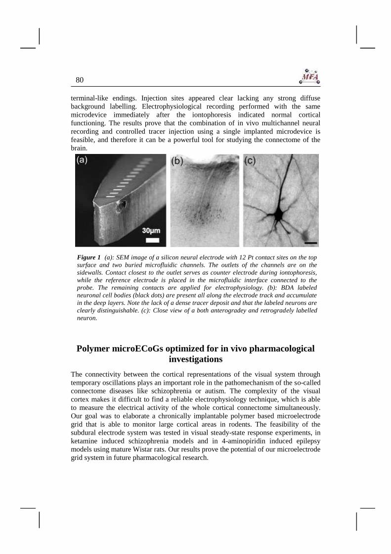
80
terminal-like endings. Injection sites appeared clear lacking any strong diffuse
background labelling. Electrophysiological recording performed with the same
microdevice immediately after the iontophoresis indicated normal cortical
functioning. The results prove that the combination of in vivo multichannel neural
recording and controlled tracer injection using a single implanted microdevice is
feasible, and therefore it can be a powerful tool for studying the connectome of the
brain.
Figure 1 (a): SEM image of a silicon neural electrode with 12 Pt contact sites on the top
surface and two buried microfluidic channels. The outlets of the channels are on the
sidewalls. Contact closest to the outlet serves as counter electrode during iontophoresis,
while the reference electrode is placed in the microfluidic interface connected to the
probe. The remaining contacts are applied for electrophysiology. (b): BDA labeled
neuronal cell bodies (black dots) are present all along the electrode track and accumulate
in the deep layers. Note the lack of a dense tracer deposit and that the labeled neurons are
clearly distinguishable. (c): Close view of a both anterogradey and retrogradely labelled
neuron.
Polymer microECoGs optimized for in vivo pharmacological
investigations
The connectivity between the cortical representations of the visual system through
temporary oscillations plays an important role in the pathomechanism of the so-called
connectome diseases like schizophrenia or autism. The complexity of the visual
cortex makes it difficult to find a reliable electrophysiology technique, which is able
to measure the electrical activity of the whole cortical connectome simultaneously.
Our goal was to elaborate a chronically implantable polymer based microelectrode
grid that is able to monitor large cortical areas in rodents. The feasibility of the
subdural electrode system was tested in visual steady-state response experiments, in
ketamine induced schizophrenia models and in 4-aminopiridin induced epilepsy
models using mature Wistar rats. Our results prove the potential of our microelectrode
grid system in future pharmacological research.

Yearbook 2015
81
Figure 1 Schematic of rat skull with the implantation sites of the microgrid (left). Our
polymer microgrid during surgery (right).
Figure 2 Ketamine induced dissociation state in schizophrenia animal model. Red and
blue area represent spectral power density in a control period (10s) and after ketamine
injection (10s). Measurements were using a 32-channel microelectrode grid directly
placed on the visual cortex. Fig. 4: EEG recorded by our microgrid during an epileptic
seizure after 4-AP injection.

82
In vitro studies revealing the immune response of the living
tissue to nanostructured implant surfaces
Our goal is to design and fabricate nanostructured surfaces to reduce the extent of
glial cell encapsulation of Central Nervous System implants and to promote neural
attachment and regeneration, which improve the biocompatibility and functionality of
the interfaces. Recent findings showed that specific glial cells prefer flat surfaces over
nanostructured ones with certain geometries, while neural cells proliferate both on
nanostructured and flat surfaces.
Figure 1 Two channel fluorescent images of GFP-NE-4C cells on nanostroctured chips
after 24h adhesion (blue channel: DAPI staining - cell nuclei; green channel: green light is
emitted by the GFP expressed in the cytoplasma). Black regions are the nanostructured
patterns on the samples. Inset images show the transition region, where flat poly-Si regions
meet the nanostructured Si grass. Nanostructured surfaces are less preferred by the NE-4C
cells compared to flat regions.
Figure 2 Comparison of cell counts after 4 hr and 24 hr long incubation of NE-4C neural
progenitor cells on different surface types (nanostructured Si, nanostructured Pt, flat Pt
and glass). Nanostructured regions hinders the adhesion of the stem cells compared to
their flat references.
Neural progenitor cells were cultured on flat and nanostructured Si and Pt surfaces.
Based on the MTT tests, the nanostructured surfaces are non-toxic compared to the
glass surfaces. Cell adhesion was hindered by the nanostructured surfaces compared
to the flat ones. Analysis of fluorescent microscopy images suggests that the cell
number increases on every investigated surface type (Si nanograss, Pt, nano-
structured Pt, glass), however, the proliferation is slower on nanostructured regions.

Yearbook 2015
83
NEMS
Activity leader: J. Volk
Group members: Zs. Baji, G. Battistig, Cs. Dücső, P. Földesy, N. Q. Khánh, I.
Lukács, Gy. Molnár, A. L. Tóth, Zs. Zolnai, R. Erdélyi, Z. Szabó, and I. Bársony
Projects:
OTKA K108869 – “Széles tiltott sávú félvezető anyagok, nanoszerkezetek és
korszerű eszközök”
OTKA K112114 – “Kombinált mikro-nanotechnológiai eljárások és ellenőrzésük
lokális analitikai technikákkal: a mintázatképzéstől az alkalmazások felé”
FP7-ICT-2013-10- 611019 – “High-resolution fingerprint sensing with vertical
piezoelectric nanowire matrices (PiezoMAT)”
Homogeneous transparent conductive ZnO:Ga by ALD for
large LED wafers
Transparent conductive oxides are widely used in photovoltaics, thin film transistors
and light emitting devices. The most common TCO material is indium doped tin
oxide (ITO), but in the past decades the price of indium has been rapidly increasing.
One of the most promising replacements due to its excellent transparency in the
visible wavelength range and similar electrical conductivity is highly n-doped zinc
oxide. Ga doped ZnO (GZO) has an excellent transparency and low resistivity
combined with an electrical stability at elevated temperatures and excellent crystalline
properties. Atomic layer deposition (ALD) is a promising candidate to produce high
quality GZO layers at relatively low temperatures (300 °C) and at large wafer sizes as
well.
We used atomic layer deposition to acquire a series of GZO thin films with varying
nominal Ga concentrations. Homogeneity tests were carried out on GZO thin films
deposited on a 4” glass wafer. The effect of the annealing and the fabricated devices
were investigated on GZO layers deposited on a commercial InGaN/GaN LED-wafer,
whereas for electric and electroluminescence measurements fully processed GZO
coated LED-chips were used. We also tried a number of different thermal annealing
processes to gain a film with properties optimized for LED applications.
To find the optimal concentration, GZO/c-sapphire films with Ga concentrations of
1, 2, 3, 4, 5, and 10 at% were used. According to the Hall measurements, the
increasing doping level reduces the specific resistivity of the layers down to 3.3×10⁻⁴
cm at 3 at% then it increases monotonously with the growing doping concentration.
This behavior is governed mainly by the change in free carrier concentration: The
doping increases the free carrier concentration up to 1.38×1021 cm-3, until reaching an
optimal Ga content of 3 at%. In this regime the volume concentration of Ga is close to
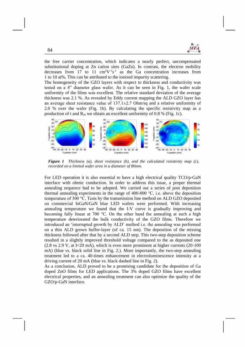
84
the free carrier concentration, which indicates a nearly perfect, uncompensated
substitutional doping at Zn cation sites (GaZn). In contrast, the electron mobility
decreases from 17 to 11 cm2V-1s-1 as the Ga concentration increases from
1 to 10 at%. This can be attributed to the ionized impurity scattering.
The homogeneity of the GZO layers with respect to thickness and conductivity was
tested on a 4” diameter glass wafer. As it can be seen in Fig. 1, the wafer scale
uniformity of the films was excellent. The relative standard deviation of the average
thickness was 2.1 %. As revealed by Eddy current mapping the ALD GZO layer has
an average sheet resistance value of 137.1±2.7 Ohm/sq and a relative uniformity of
2.0 % over the wafer (Fig. 1b). By calculating the specific resistivity map as a
production of t and Rsh we obtain an excellent uniformity of 0.8 % (Fig. 1c).
Figure 1 Thickness (a), sheet resistance (b), and the calculated resistivity map (c),
recorded on a limited wafer area in a diameter of 80mm.
For LED operation it is also essential to have a high electrical quality TCO/p-GaN
interface with ohmic conduction. In order to address this issue, a proper thermal
annealing sequence had to be adopted. We carried out a series of post deposition
thermal annealing experiments in the range of 400-800 °C, i.e. above the deposition
temperature of 300 °C. Tests by the transmission line method on ALD GZO deposited
on commercial InGaN/GaN blue LED wafers were performed. With increasing
annealing temperature we found that the I-V curve is gradually improving and
becoming fully linear at 700 °C. On the other hand the annealing at such a high
temperature deteriorated the bulk conductivity of the GZO films. Therefore we
introduced an ‘interrupted growth by ALD’ method i.e. the annealing was performed
on a thin ALD grown buffer-layer (of ca. 15 nm). The deposition of the missing
thickness followed after that by a second ALD step. This two-step deposition scheme
resulted in a slightly improved threshold voltage compared to the as deposited one
(2.8 vs 2.9 V, at I=20 mA), which is even more prominent at higher currents (20-100
mA) (blue vs. black solid line in Fig. 2.). More importantly, the two-step annealing
treatment led to a ca. 40-times enhancement in electroluminescence intensity at a
driving current of 20 mA (blue vs. black dashed line in Fig. 2).
As a conclusion, ALD proved to be a promising candidate for the deposition of Ga
doped ZnO films for LED applications. The 3% doped GZO films have excellent
electrical properties, and an annealing treatment can also optimize the quality of the
GZO/p-GaN interface.

Yearbook 2015
85
Figure 2 Voltage (left vertical axis) and output electroluminescence intensity (right
vertical axis) as a function of driving current recorded on the LEDs for the thin (ca. 45
nm) non-annealed (black) and 2-step deposited annealed GZO TCO (blue), respectively.
Double Markers for Direct Contact Formation on Ultra-Low
Dimension Objects
For contact formation on very small objects, like TiO2 nanowires (NWs) with ultra-
low dimensions (few nm wide and few tens nm long), determination of the
coordinates of the objects in a pre-deposited marker array is a challenge. Thin NWs
are hard to see by Scanning Electron Microscopy (SEM), because of weak contrast.
Also, the sample becomes contaminated fast at such high SEM magnification.
So far, we carried out very thin metal contact pairs formation with very narrow gap
(few tens of nm) to avoid the problem mentioned above. Then Atomic Force
Microscope (AFM) has been used to find the adequate NWs, which were accidently
contacted at both ends. Later on, the second metal is to be deposited to make a
connection between the leads and the contact pairs. This approach therefore, is very
time-consuming due to large number of AFM measurement. Also, the NW’s location
to the contact is not well controlled. With the new facility (RAITH 150), we have
developed a novel technique, where we use a double marker array to enable the
contact formation directly on a selected NW.
In our new approach, the thick markers are used to give sufficient contrast of SEM
image for alignment at e-beam lithography, while the thinner ones ensure fast
determination of the wire coordinates by AFM. The main steps of the procedure are
followings:

86
Thick marker formation by e-beam lithography and metal deposition. Markers are
exposed during alignment procedure, so the thick markers ought not to be located
close to the object to be processed
Thin marker formation with alignment on thick markers
AFM measurement at thin makers
Object selection and contact design based on the AFM images
Contact formation using thick markers
Despite of uncertainties (errors at thick marker alignments, drift in AFM
measurements), the results of all NWs of the batch (8 NWs) are acceptable as seen on
Fig. 1.
Figure 1 AFM image of the NW to be contacted indicated by the arrow, the contact
design is also shown. Part of the thin marker can be seen on the top of the image (left).
Contacted NW with ca. 24 nm gap (right).

Yearbook 2015
87
Thin Film Physics Department
Head: Dr. Béla PÉCZ, D.Sc., Scientific Advisor
Research Staff
Katalin BALÁZSI, Ph.D., Deputy Head
of Department
Ildikó CORA, Ph.D.
Zsolt CZIGÁNY, D.Sc.
László DOBOS, Ph.D.
András KOVÁCS, Ph.D., (on leave:
Ernst-Ruska Centrum, Jülich)
Viktória KOVÁCSNÉ-KIS, Ph.D.
Miklós MENYHÁRD, D.Sc.
(Prof. Emeritus)
Fanni MISJÁK, Ph.D.
György RADNÓCZI, D.Sc.
György Zoltán RADNÓCZI, Ph.D.
György SÁFRÁN, C.Sc.
Attila SULYOK, Ph.D.
Péter SÜLE, Ph.D.
Lajos TÓTH, C.Sc.
Orsolya TAPASZTÓ, Ph.D.
Árpád BARNA, D.Sc., emeritus inst.
Péter B. BARNA, D.Sc., emeritus inst.
György GERGELY, D.Sc., emeritus inst.
Ph.D. students
Zsolt FOGARASSY
Ákos Koppány KISS
János SZÍVÓS
Nikolett OLÁH
Márton SZENDRŐ
Erzsébet DÓDONY
Technical Staff
Noémi SZÁSZ
Sándor GURBÁN
Andor KOVÁCS
István KOVÁCS
Katalin PUSKÁS (50%)
Viktor VARGA
Fenyvesiné Andrea JAKAB
Valéria OSVÁTH (50%)
Thin Film Physics Department was dealing with numerous subjects in 2015; four
main research areas were in focus. The first one was the study of the structure
evolution in polycrystalline layers, development of thin coatings, and layers for hard
coatings, for magnetic layers and for composites. Development of biocompatible
surgical implants was also an important part of this area. The first results on high
entropy alloys were achieved. Second main subject was the research of
semiconductor layers, heterostructures. The morphology of graphene which
influences the electronic properties was determined. After a project was successfully
finished on heat management in high power gallium nitride devices, papers with high
recognition were published on the heat conductivity of diamond. A lot of new
information was collected how nickel can induce crystallization of amorphous silicon.
The third main field of study was the development of methodology in electron
diffraction and on ion-solid interactions. The most recent results presented tools for

88
the description of grain boundaries based on electron precession on grain boundary
characterization based on electron diffraction. The last subject studied was the
development of ceramic/graphene nanocomposites by powder technology for
tribological applications in aqueous environments.
In 2015, 28 papers were published in refereed journals with cumulative impact factor
of 91, and additional 15 papers in conference publications with no impact factor. The
members of the group presented 8 invited lectures, 15 oral talks and 23 posters at
international conferences. The group received 1400 independent citations in the
examined interval of the last two years.
Summarizing other activities, members of the group lectured three theoretical courses
at universities and four members held laboratory practices, all courses were for full
semesters (ELTE, BME). Additionally, 12 weeks of summer practice and special labs
were also conducted. In addition to the 5 Ph.D. students, 3 diploma workers were also
supervised.
Social activity of the group is landmarked by 15 memberships in different committees
of the Hungarian Academy of Sciences (HAS) and of boards of societies, giving two
elected representatives to the General Assembly of the Academy of Sciences.
Our colleauge, Prof. Peter B. Barna received for his lifetime achievements the
prestigious R. F. Bunshah Award (http://www.mfa.kfki.hu/hu/node/827/).
New approaches in the development of Hypoallergenic implant
material in Orthopedics: steps to personalised medicine
(OTKA 105355, EU FP7 HypOrth)
K. Balázsi, O. Tapasztó, N. Oláh, Zs. Fogarassy, V. Varga, D. Delfonse (Mathys, Switzerland), C. Lohman (Magdeburg Un., Germany), J. Lorenzen (Teknologisk
Institute, Denmark), M. Ignatiev (INOP, Poland), and Cs. Balázsi
The European collaborative project HypOrth (http://www.hyporth.eu/) aims to
develop hypoallergenic material for endoprostheses, pursuing two major goals:
HypOrth intends to improve the understanding and diagnosis of complications
associated with an implant, primarily focussing on adverse immune reaction and
infection. Based on these insights the project is developing innovative approaches for
renewals in orthopaedic arthroplasty with improved biocompatibility.
The project central database allows the compilation of all relevant data and brings
together clinical and scientific results. These data are also available to material
researchers and developers. For patients with the risk of getting an adverse immune
reaction to conventional material composition we developed a new material
combination with hypoallergenic and antibacterial properties and a new
hypoallergenic endoprosthesis prototype.
The materials used for artificial prosthesis by default are Titanium (TiAl6V4,
TiAl6Nb7 – forged alloy), CoCrMo (forged alloy), ceramics and UHMWPE (Ultra
High Molecular Weight PolyEthylene).

Yearbook 2015
89
The role of Thin Film Physics Department is the development of novel ceramic
coatings for existing Mathys implants. The main part of research is confidential.
Characterization of biocompatible ceramic TiC / amorphous C
thin films prepared by DC magnetron sputtering
(EU FP7 „HypOrth 602398: New approaches in the development of
Hypoallergenic implant material in Orthopaedics: steps to personalised
medicine)
N. Oláh, Zs. Fogarassy, A. Sulyok, J.Szívós, M. Veres (Wigner Research Centre for Physics), G. Kaptay (Bay Zoltán Nonprofit Ltd for Applied Research), T. Csanádi (IMR
SAS, Slovakia), and K. Balázsi
Over the last few years, TiC/a:C nanocomposite protective surface coatings,
consisting of hard TiC nanoparticles embedded in a soft amorphous matrix, have
attracted a special attention because of their passivation effect on different implant
materials. Therefore, our development is focused on the biological application of
these thin films [http://www.hyporth.eu/].
Figure 1 Structure of TiC/a:C films by HRTEM deposited at 5 and 70 W of Ti target
power (left) and the measured mole fraction of Ti in the deposited layer (over) and the
measured mole fraction of amorphous carbon in the deposited layer (under).

90
The main goal of our research work is the understanding of deposited TiC/a:C growth
mechanism and the determination of TiC crystal formation at different Ti:C ratios. A
secondary aim was to investigate the relationship between the exact elemental
composition and mechanical and tribological properties of the different films.
TiC/a:C thin films were prepared by DC magnetron sputtering. The detailed
preparation steps of the coatings were described in our previous works [N. Oláh, M.
Veres, A. Sulyok, et al., J Eur Ceram Soc. 34(14) (2014) 3421-3425], [N. Oláh, Zs.
Fogarassy, et al., Ceram. Inter. 41(4) (2014) 5863-5871]. Magnetron sputtering of
carbon and titanium were performed simultaneously. The film´s composition and
morphology were studied in details by High Resolution Transmission Electron
Microscopy (HRTEM), X-ray photoelectron spectroscopy (XPS) and Raman
spectroscopy. The mechanical characteristics of the TiC/a:C thin films were
investigated by nanoindentation technique while the tribological behavior of the films
was examined by a ball-on-disk tester (CSM tribometer) moving on circular trajectory
at room temperature.
Very good agreement was observed between theoretical calculations and
experimental measurements. The thickness of amorphous carbon matrix decreased
simultaneously with the increasing Ti content. The amorphous carbon has not gone
through to a graphitization process. The highest hardness (H) of ~ 26 GPa and
modulus of elasticity (E) of ~ 140 GPa with friction coefficient of 0.268 was observed
in case of the film prepared at ~ 40 at% Ti content (by XPS) which consisted of 4-10
nm width TiC columns separated by 2-3 nm thin a:C layers. The H3/E2 ratio was 0.9
GPa that predicts high resistance to plastic deformation of the C-Ti nanocomposites
beside moderate wear-resistant properties (H/E=0.19).
Graphene-ceramic composites for tribological application in
aqueous environments
(OTKA M-ERANET “Grace”)
O. Tapasztó, Zs. Fogarassy, V. Varga, C. Balázsi (Bay Zoltán Ltd, Hungary), J. Dusza (IMR SAS, Slovakia), A. Kailer (IMW Franhoufer, Germany), and K. Balázsi
Advanced ceramic materials have proved their superior wear resistance as well as
mechanical and chemical properties in a wide range of industrial applications. Today
there are standard materials for components and tools that are exposed to severe
tribological, thermal or corrosive conditions. The main aim of the project is to
develop novel, highly efficient tribological systems on the basis of functionalized
graphene and ceramic-graphene-nanocomposites and to prove their superior quality
and suitability for technical applications e.g., for slide bearings and face seals in
aqueous media.
Current research in the field of ceramic nanocomposites shows that is possible to
make ceramic materials with improved mechanical and tribological properties by
incorporating graphene into the ceramic microstructure. The electric conductivity of

Yearbook 2015
91
these materials, which is reached already at low graphene contents, offers the
possibility to reduce efforts in manufacture and to create new functions that may be
utilized in technical applications.
Figure 1a Milled and hot pressed
Si3N4 composite with 10 wt% MLG.
Figure 1b Milled and hot pressed Si3N4
composite with 10 wt% MLG.
Multilayered graphene (MLG) was prepared by attritor milling technique. 10 hours
intensive milling of 1 and 5 micrometer sized graphite powders yielded MLG with
20-30 layers. The large quantity, very cheap and quick preparation process is a main
strength of our MLG. Si3N4 / graphene nanocomposites prepared by attritor milling
and sintered by spark plasma sintering (SPS, partner IMR SAS, Fig. 1a) and hot
pressing (HP, partner IMR SAS, Fig. 1b). The Si3N4 with 1wt%, 3wt%, 5wt% and
10wt% MLG were produced and their structure was fully examined by our
department.
This new approach is very promising, since ceramic microstructures can be designed,
that are electrically conductive, possess high toughness and provide improved wear
resistance at low friction. Furthermore, electrical conductivity can be utilized for
monitoring and electrochemical protection devices.

92
Low cycle thermomechanical fatigue of a reactor steel:
microstructural investigations
(TAMOP 4.2.2.A-11/1 /KONV-2012-0027, Dunaújvárosi Egyetem)
B. Fekete1,2, F. Misják3, P. Trampus1, and G. Radnóczi3
1College of Dunaújváros, Táncsics u. 1A, Dunaújváros, H-2400 Hungary 2 Deptment of Applied Mechanics, Budapest University of Technology and
Economics,Műegyetem rakpart 5, Budapest, H-1111 Hungary 3MTA EK MFA, 1121 Budapest, Konkoly-Thege M. u. 29-33
One of the possible damage mechanisms in pressurized water reactors is the low cycle
thermomechanical fatigue caused by simultaneous thermal and mechanical loading,
during transient operating processes (e.g., at start up and shut down) and accident
conditions. The reactor pressure vessel has a key role in the safety of the nuclear
power plant operation and possible lifetime extension. It is necessary to ensure the
integrity of the reactor pressure vessel during normal and off-normal operating
conditions, so the knowledge on low cycle fatigue degradation phenomena is
important. In this work we investigated the thermomechanical low cycle fatigue
behaviour of the VVER-440 reactor pressure vessel structural materials. Low cycle
continuous and interrupted thermomechanical fatigue tests were made on the base
metal (15Ch2MFA) of the vessel at parameters corresponding to the exploitation
conditions in the reactor. The measurements were carried out at thermo-mechanical
fatigue conditions in the range of 150-270 oC using the GEEBLE 3800 mechanical
simulator. All fatigue tests were carried out with a symmetric cyclic strain and a
triangular waveform at frequency of 0.083 Hz. The longitudinal total strain amplitude
level was 0.3 %. The lifetime of the material was determined to be 2376 cycles.
Interrupted fatigue tests were carried out to investigate the kinetics of the fatigue
softening of the material at different stages of its lifetime.
Transmission electron microscopy measurements made at different stages of fatigue
test show that the dislocation concentration after an initial increase starts decreasing
(Fig. 1). At about 50 % of the nominal lifetime the structure of grain and cell
boundaries changes from strained to relaxed, i.e. the strain field of captured
dislocations (Fig. 2a) dynamically disappears. The recovery of dislocation
substructure resulted in decrease of dislocation density accompanied with boundary
movements, which are well seen in the TEM images (Fig 2b). The reduction of
dislocation density can be a result of two simultaneously operating mechanisms:
annihilation during movement and entrapment in cell boundaries. Then the micro-
deformation process will be continued in the grain boundaries, where micro cracks
initiate.
The investigated low cycle fatigue behaviour can provide reference for remaining life
assessment and lifetime extension analysis of Nuclear Power Plant components.

Yearbook 2015
93
Figure 1 The variation of dislocation density as the function of the lifetime under thermo-
mechanical treatment. (The X-ray measurement was performed at the Eötvös University
by Bertalan Jóni.)
Figure 2 TEM image of the grain/cell structure of 15Ch2MFA steel after thermo-
mechanical fatigue for 5% (right) and 50% (left) of lifetime.

94
Characterization of defect structure in electrodeposited
nanocrystalline Ni films
T. Kolonits (MFA), P. Jenei (ELTE), B.G. Tóth (Wigner), Zs. Czigány (MFA), J. Gubicza (ELTE), L. Péter (Wigner), and I. Bakonyi (Wigner)
The effect of organic additives (saccharin and formic acid) on the defect structure in
electrodeposited Ni films was investigated by X-ray diffraction (XRD) line profile
analysis (eCMWP model) and transmission electron microscopy (TEM) [64]. The
main task of the project is to investigate the effect of the additives on the grain
structure and defect (dislocation and twin) density which influence the macroscopic
properties and application of the layers. The electrodeposited layers were deposited at
room temperature at a current density of j= -43.75mA/cm2. The basic electrolyte
contained 0.6 mol/ℓ nickel sulphate (NiSO4·7 H2O), 0.30 mol/ℓ sodium sulphate
(Na2SO4·10 H2O), 0.25 mol/ℓ H3BO3 és 0.15 mol/ℓ H3NO3. The 46 mℓ/ℓ formic acid
or 1 g/ℓ saccharine was mixed into this bath.
Figure 1 Grain size distribution of nanocrystalline Ni film deposited with formic acid
additives determined by TEM and XRD. The grain size refinement is shown in TEM images
and electron diffractions. Nanotwins observed in the film deposited with saccharine are
illustrated in the HRTEM image.
In the film deposited without additives, a columnar structure was observed showing
similarities to the T-zone of structure zone models. The typical column width was
~120nm and their length was >3m. There was no detectable twinning. Both formic
acid and saccharin additives resulted in equiaxed grains with reduced size, as well as
increased dislocation and twin fault densities in the nanocrystalline films (Fig. 1).
Moreover, the structure became homogeneous and free of texture within the total film
thickness due to the additives. Saccharin yielded smaller grain size and larger defect
density than formic acid. The inhibiting effect of the additives can be attributed to the
surface coverage of the hydrophilic functional groups. The incorporation of ~0.3at%
sulphur was detected only in the films deposited with saccharine which imply
different mechanisms for the two additives. In the layers deposited with formic acid
no incorporated contamination was detected by EDS. A detailed analysis of the grain

Yearbook 2015
95
size and twin boundary spacing distributions was also carried out with the
complementary application of TEM and XRD (Fig. 1). It is important to mark the
difference between the grain size – determined by TEM and the crystallite size -
determined by XRD. The reason of the difference is the high sensitivity of XRD for
the small orientation differences due to different kind of crystal defects. Generally the
grain size is approximately 2 times larger than the crystallite size. The defect density
distributions determined by TEM and XRD showed similar tendencies. Presumptions
of the eCMWP model about the grain size distribution (lognormal) were confirmed
by TEM. Twin-boundary spacing follows geometric distribution for large spacing
values in accordance with the model used in the XRD line profile analysis. However,
for twin-boundary spacing smaller than 5 nm, TEM yields a smaller fraction than that
predicted by XRD which discrepancy is due to the presence of numerous nanotwins
as evidenced by HRTEM (Fig.1).
Characterization of the topography of the graphene moiré
superlattice on Au(111) and Cu(111) supports
(OTKA K112811, OTKA K108753, KHJLN)
P. Süle, M. Szendrő, G. Magda, C. Hwang, and L. Tapasztó
In the last two years, we reached remarkable results in the theoretical and
experimental study of surface morphology of graphene [124,125], [P Süle, at.al:
Carbon 77, 1082-1089 (2014)]. Graphene moiré superlattices formed on various
hexagonal supports (e.g. 111 metal surfaces) exhibit convex (protruded) morphology.
In rare cases, suspected to be concave (nanomesh with periodic lattice of depressions)
topography may exist. However, the experimental verification of the topography
convexity is difficult. The curvature of the surface topography can not be clearly
specified by STM due to the bias voltage dependence of the measured convexity.
Varying the bias voltage contrast inversion occurs which prevents the unambiguous
identification of the surface curvature. Using additional first principles DFT
theoretical studies were only able to prove the existence of convex morphology e.g.
on Ru(0001). Why is it important to know the precise topographic curvature of the
graphene surface? According to our present knowledge and assumptions convex and
concave superlattices may exhibit different electronic structure properties such as
LDOS or band structure. Moreover, the surface activity, such as the adsorption energy
of various molecules and/or the local magnetic property of surface Carbon atoms may
depend on the morphology of the superlattice.
The most important results:
The detailed description of the topography of moiré superlattices using a
combined theoretical and STM approach [124,125].

96
The coexistence of convex and concave superlattices has been explored in the
same image which rules out the presence of contrast inversion [124]
DFT calculations support the possible coexistence of various superlattices with
different curvature due to the tiny energy difference between the various
morphologies [124]
The Au(111) surface reconstructs upon graphene adsorption and exhibits an
imprinted topography very similar to that of the moiré superlattice [124]
Figure 1 Concave (a) and convex (b) graphene moiré superlattices as computed by
molecular dynamics simulations.
Figure 2 Concave graphene superlattice (nanomesh) on a herringbone reconstructed
Au(111) surface. Topographic images as obtained by STM (a) and by molecular
dynamics simulations (b).

Yearbook 2015
97
Microscopy of high quality cubic SiC grown on Si
(OTKA K 108869 and bilateral agreement between CNR and MTA)
M. Bosi1, G. Attolini1, M. Negri1, C. Ferrari1, E. Buffagni1, C. Frigeri1, M. Calicchio1, B. Pécz2, F. Riesz2 , I. Cora2, Z. Osváth2, L. Jiang3, and G. Borionetti4
1 IMEM-CNR, Parco Area delle Scienze 37 A, 43124 Parma, Italy 2 MTA EK MFA, P.O.Box 49, H-1525 Budapest, Hungary
3 Engineering Sciences, Faculty of Engineering and the Environment, University of Southampton, Highfield, Southampton SO17 1BJ, United Kingdom
4 MEMC Electronic Materials S.p.A., Viale Gherzi 31, 28100 Novara, Italy
Cubic silicon carbide (-SiC or 3C-SiC) is a wide-bandgap semiconductor with high
hardness, high electron mobility, high thermal conductivity, high resistance to
chemical attack and it is biocompatible; for these reasons SiC is interesting for
potential technological applications, such as power devices and sensors operating in
harsh environments. The growth of this polytype is a challenge.
Several samples were grown by varying the deposition temperature and the MTS
(monomethylsilane, CH3SiH3) content in order to study how these parameters affect
the layer quality and the lattice defects. The use of single source precursor (like MTS)
increases the growth rate of SiC.
The grown layers were investigated by several techniques including transmission
electron microscopy (TEM), Makyoh analysis and Raman spectroscopy. The TEM
specimens were prepare dby Ar ion milling and then investigated by conventional and
high resolution microscopy.
Figure 1 Bright field (left) and dark field (right) images taken on a sample grown with the
addition of MTS. Diffraction pattern is inserted to the middle of the above image.
The TEM images in Fig. 1 show the sample grown at 1400 °C with the addition of
MTS. The single crystalline SiC layer contains a lot of stacking faults, which give
faint streaks in the diffraction pattern. There is a huge density of defects at the SiC/Si
interface, which is however, decreased substantially toward the surface.
When we compare a sample grown at the same temperature, however, without the
addition of MTS we can observe that the defect density is higher than the previous
sample. Beside the well-known stacking faults there were antiphase boundaries inside
SiC. The layer is single crystalline as well, but the defect density is not decreased so

98
much like in the former case toward the surface. Low magnification images had
shown that the surface of the grown SiC layer is not perfectly flat.
Although in all of the grown SiC layers the defect density is high close to the silicon
substrate, we observed that in layers grown with the addition of MTS (both at
1300 °C and at 1400 °C) the defect density is substantially lowered towards the
surface region. This observation was supported by the Raman analysis based on the
shift of the Raman peaks, as well.
Metal (Ni) induced crystallization in amorphous Si thin films
(TÉT-10-1-2011-0570)
Gy. Z. Radnóczi, E. Dódony, G. Battistig, B. Pécz, I. Stoimenos, N. Frangis, and N. Vouroutzis (AU, Thessaloniki)
The formation of various silicide phases was studied to understand the initial stages of
Ni induced crystallization of amorphous silicon (a-Si). During the experiments
presented here only silicide formation occurred as the Ni supply was practically
unlimited in comparison to the a-Si film.
Figure 1 The result of in-situ heat treatment of a Si film with native oxide layer (left) and
a Si film cleaned with HF solution (right).
The previously developed model system for in situ experiments was used. The
amorphous Si foil on Ni microgrid proved to be a stable and reliable system for the
investigation of silicide formation at elevated temperatures; however, some concerns
were raised about the native oxide on the surface of the Si film. This thin oxide is
believed to hinder the Ni diffusion into the Si film and it is also a relevant difference
with respect to the usual MILC structures which contain no oxide film between the Ni

Yearbook 2015
99
and Si. To eliminate this potential diffusion barrier the Si film was transferred to a HF
solution before placing it onto the Ni grid. The Ni grids were also cleaned in an
etching solution (NH4OH). In situ experiments were carried out with the new
structures. The resulting structure was different from the structures obtained in our
earlier experiments. For a comparison see Fig. 1.
Figure 2 Ni(red) and O (green) elemental maps (left) of a whisker combined into a single
image. The map shows a Ni containing whisker with a (silicon)oxide shell. The bright field
micrograph of a whisker is shown on the right).
In contrast to previous results whiskers were observed in the new structures (Fig. 2).
The whiskers were growing out of the plane of the a-Si film as determined by stereo
images recorded with 8° tilt difference. The analysis of the whiskers showed that they
consist of Ni2Si phase and they also have an oxide shell as revealed by analytical
measurement carried out by Austrian partners within ESTEEM project.
A report on the above experiments and other results obtained in low temperature
annealing of MILC structures was published recently [G. Z. Radnóczi, et al:
Structural characterization of nanostructures grown by Ni metal induced lateral
crystallization of amorphous-Si, Journal of Applied Physics 119, 065303 (2016),
DOI:10.1063/1.4941349] and further work is in progress on characterization of Si
whiskers obtained at low temperature.
A universal nanopatterning technique using RF plasma etching
through templates of Langmuir-Blodgett films
J. Szívós, M. Serényi, Sz. Pothorszky, G. Vértesy, and G. Sáfrán
The nanoscale modification of materials has attracted wide research interest recently.
At present, mostly, slow and expensive methods are available for the fabrication of
ordered nanostructures. Last year a cheap and fast technique was proposed [J. Szívós,
et al: Nanopattern formation in UV laser treated a-AlOx and nc-Al/AlOx layers,
Vacuum 109, 200 (2014)] to produce ordered nanopatterns directly or to prepare

100
masks for nanolithography and nanoimprint molds. This technique applies a
monolayer of hexagonally self-assembled silica nanospheres (Langmuir-Blodgett
(LB) film) as a template and the sample surface is treated by a single UV laser
(=248 nm) pulse through the LB film. We could produce nano-patterned Al-oxide
layers by this technique successfully. Experiments were carried out in 2015, however,
it was found that UV laser patterning is hardly effective in case of metal surfaces: the
pattern with a pale contrast in the scanning electron microscope image (shown in
Fig. 1) was so shallow that it couldn’t be visualized by cross-sectional TEM.
Figure 1 SEM image of the pattern achieved in Pt by UV laser treatment. Some residual
nanoballs of the LB film are seen at the left side.
The reason of the inefficiency is the absorption mechanism of the UV laser in metals:
the (quasi-)free electrons are thermalizing the lattice, thus the whole metal surface
absorbs the energy nearly uniformly [M. S. Brown, C. B. Arnold: Fundamentals of
Laser-Material Interaction and Application to Multiscale Surface Modification,
Springer Series in Materials Science Volume 135, 91-120 (2010)] despite the
presence of the LB film. It is likely that femtosecond pulse length would be required
to avoid this effect.
The aim of the PhD work is to find simple, cheap and fast solution for nanoscale
patterning of metallic, as well magnetic layers. The latter allows increasing the
capacity of FePt or CoPt magnetic recording media by the preparation of ordered
nanopatterns thus realizing Bit Patterned Media (BPM).
The LB film is suitable to prepare ordered, self-assembled template at large areas.
The goal was to transfer the pattern of the template to a wide range of materials.
Experiments with 30 kV ion-implantation have shown that in the case of metals the
energy (and flux) of the applied ions (Ar+, possibly Xe+) is not sufficient. RF plasma

Yearbook 2015
101
etching, however, proved to be very effective that led to a universal technique capable
to nanopattern various materials, e.g. oxides, semiconductors and metals.
The LB film-covered sample is placed at the „target” position of the RF sputtering
source 40 mm far from the ground plate and is subjected to 1 kV Ar plasma with
pressure 2.5 Pa. The nanospheres of the LB film protect the surface and sputtering
takes place between the nanospheres. This way the hexagonal pattern of the LB film
can be replicated to almost any material’s surface provided that the plasma
parameters and etching time are well set. The feature size is determined by the
diameter of the nanospheres that, in principle, can be scaled down to about 10 nm.
In order to demonstrate the operability of the technique and the effects of changing
the plasma parameters DC magnetron sputtered Pt thin films were nanopatterned. Pt
layers are widely utilized e. g. for masking. It is suggested that Pt has a sputtering rate
similar to that of FePt and CoPt.
Based on TEM investigations the layer structure of our Pt samples was the following:
Si(001) substrate/thermal SiOx (1140±10nm)/TiOx buffer (11.3±0.3nm)/35±4nm Pt.
A pattern fabricated with optimum parameters is shown in Fig. 2. In (a) the SEM
image shows the patterned Pt layer itself. Hexagonally arranged pattern is shown up,
but the domains and stacking faults of the LB film are replicated as well.
Figure 2 The pattern prepared by our RF plasma etching technique in the Pt layer. Plan
view SEM (a) and cross-section TEM (b) images.
The cross-sectional TEM image in Fig. 2 (b) represents part of the SiOx underlayer,
the Pt with the plasma etched pits and the residue of the 100 nm diameter nanospheres
of the LB film that protected the layer beneath.
Nanopatterning with RF plasma through an LB film is a fast and cheap technique that
may be suitable, as well, for mass production. Our plans for 2016 are to study, in
collaboration with our Japanese colleagues, the magnetic properties of such
nanopatterned L10 CoPt thin films. That can be an alternative implementation of bit
patterned magnetic media.
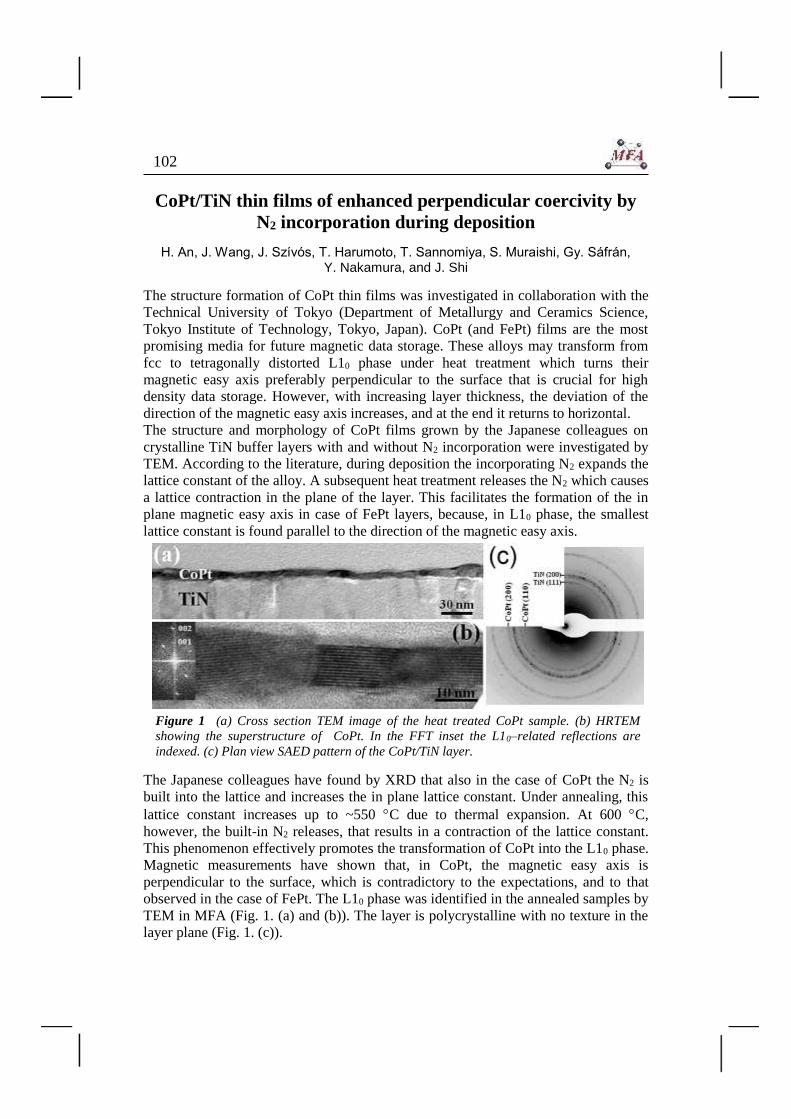
102
CoPt/TiN thin films of enhanced perpendicular coercivity by
N2 incorporation during deposition
H. An, J. Wang, J. Szívós, T. Harumoto, T. Sannomiya, S. Muraishi, Gy. Sáfrán, Y. Nakamura, and J. Shi
The structure formation of CoPt thin films was investigated in collaboration with the
Technical University of Tokyo (Department of Metallurgy and Ceramics Science,
Tokyo Institute of Technology, Tokyo, Japan). CoPt (and FePt) films are the most
promising media for future magnetic data storage. These alloys may transform from
fcc to tetragonally distorted L10 phase under heat treatment which turns their
magnetic easy axis preferably perpendicular to the surface that is crucial for high
density data storage. However, with increasing layer thickness, the deviation of the
direction of the magnetic easy axis increases, and at the end it returns to horizontal.
The structure and morphology of CoPt films grown by the Japanese colleagues on
crystalline TiN buffer layers with and without N2 incorporation were investigated by
TEM. According to the literature, during deposition the incorporating N2 expands the
lattice constant of the alloy. A subsequent heat treatment releases the N2 which causes
a lattice contraction in the plane of the layer. This facilitates the formation of the in
plane magnetic easy axis in case of FePt layers, because, in L10 phase, the smallest
lattice constant is found parallel to the direction of the magnetic easy axis.
Figure 1 (a) Cross section TEM image of the heat treated CoPt sample. (b) HRTEM
showing the superstructure of CoPt. In the FFT inset the L10–related reflections are
indexed. (c) Plan view SAED pattern of the CoPt/TiN layer.
The Japanese colleagues have found by XRD that also in the case of CoPt the N2 is
built into the lattice and increases the in plane lattice constant. Under annealing, this
lattice constant increases up to ~550 C due to thermal expansion. At 600 C,
however, the built-in N2 releases, that results in a contraction of the lattice constant.
This phenomenon effectively promotes the transformation of CoPt into the L10 phase.
Magnetic measurements have shown that, in CoPt, the magnetic easy axis is
perpendicular to the surface, which is contradictory to the expectations, and to that
observed in the case of FePt. The L10 phase was identified in the annealed samples by
TEM in MFA (Fig. 1. (a) and (b)). The layer is polycrystalline with no texture in the
layer plane (Fig. 1. (c)).

Yearbook 2015
103
In one of the several existing CoPt L10 phases the lattice constant is – exceptionally –
the largest in the direction of the magnetic easy axis [U.S. Natl. Bur. Stand. Monogr.
25, 15, 168 (1978) (pdf 29-0498)]. In our samples precisely this L10 phase was found
as revealed by the intensity distribution of the selected area electron diffraction
(SAED) patterns (Fig. 2.). There is no similar phase in FePt. It follows that, in our
CoPt, the in plane shrinkage of the lattice results in an easy axis formation
perpendicular to the surface, that is favourable in magnetic recording media. The
results of the collaboration were published in JAP [5].
Figure 2 The intensity distribution of the in plane selected area electron diffraction
pattern of the heat treated sample. The layer consists of TiN, and the L10 CoPt phase.
A device for micro-combinatorial TEM studies
Gy. Sáfrán
Status of technology: The physical chemical and structural properties of the layer
systems of cutting edge technology are strongly determined by their composition. The
Binary Alloy Phase Diagrams are well explored, however, phases of thin films are
hardly studied and may remarkably differ from that of the bulk. The common
procedure to reveal the properties of concentration dependent phases is the
preparation and investigation of numerous two-component samples, one for each
CA/CB=1-A composition. This costs enormous time of man and machine.
For a study of high number of samples combinatorial methods are recognized i.e.
instead of carrying out numerous individual experiments samples of varying
composition are prepared in a single process. P. Schultz et al. [Science (1995) 268
(5218) pp.1738-1740] applied two-fold mechanical mask movement and prepared
200x200 micrometer size individual samples in various compositions at a density of
10000 sample /in2. K.E. Roskov [J. Comb. Chem. (2008) 10, pp.966–973] prepared
for different, fixed composition samples combinatorially, onto individual TEM grids.

104
The above examples are partly efficient solutions because only the preparation of
samples is combinatorial. At the Thin Films Physics Dept. of RITP an experimental
arrangement [F. Misják et al: Thin Solid Films 516 (2008) pp.3931–3934] was
implemented already as micro-combinatorial, since samples of various compositions
were both deposited and investigated in a single TEM grid: A shield with a 1mm
diameter aperture was fixed above the substrate. Two sources were facing the
substrate through the aperture at inclined angles so that the thin film was deposited at
two overlapping areas where two-component film of Ag-Cu was grown. The
drawback of that method is that the region of changing concentration is very short
(100-150 µm), the phases are accumulated and the sample does not contain the entire
(0-100%) composition range.
Objectives: The aim was to construct a micro-combinatorial device that eliminates
the incompleteness of the above solutions. The preparation and study have to be
carried out in a single TEM grid within the whole 0-100% composition range so that
the formed binary phases and variants may be well separated.
Technical design: The recently patented [Hung. Patent No. P 15 00500 (2015)]
micro-combinatorial device (Fig. 1.) incorporates a cover plate with a slit that is
moved in fine steps above the TEM grid, meanwhile the fluences of the magnetron
sources “A” and “B” are regulated adversely. This new solution provides both micro-
combinatorial preparation and investigation, so that the length of the concentration
transition increases to 1500 microns.
Figure 1 The micro-combinatorial device in operation.

Yearbook 2015
105
A TEM grid with a deposited Mn-Al micro-combinatorial sample is shown in
Fig. 2.(a). Fig 2.(b) represents energy dispersive X-ray spectrometer (EDS) data, that
aside from the edges, shows linear concentration distribution. The micro-
combinatorial sample prepared as above allows detailed and efficient analysis,
because it exhibits the entire 0-100% concentration range in a TEM grid spread along
a distance of an order of magnitude longer than earlier. The gradient of a limited
concentration range can be adjusted to arbitrarily low values for an enhanced areal
separation of the formed thin film phases. In addition, the device is suitable for the
study of the effects of parameters (residual gas pressure, temperature, etc.) that
change with time.
The author thanks J. Szívós for contributing to the measurements!
Figure 2(a) TEM grid with a microcombi-
natorial MnAl sample (1x1.5mm2) that was
deposited through a moving slit.
Figure 2(b) EDS concentration profile of
the sample in 2(a). The transition extends
to 1500µm, and the concentration range is
0-100% for both (Al, Mn) components.
Grain boundary characterization based on diffraction data
Á.K. Kiss, and J.L. Lábár
In materials science and its applications it is important to reveal the correlation
between the technique of fabrication and the resulting structure, as well as between
the structure and the properties of the materials. This is why the proper
characterization of a manufactured material is inevitable. Two newly developed
techniques are presented here, which facilitate the investigation of polycrystalline
materials with transmission electron microscope (TEM) in terms of grain boundary
characterization.
Both methods are based on computer supported measurements, which are capable of
displaying either a grain boundary network or dislocations (or both) and additionally
determining the orientation of grain boundary (GB) planes (i.e. determining their
indices expressed in the coordinate systems of either neighbouring grains). Every step
of the method (data acquisition and evaluation) is automated therefore it may serve as

106
a basis of sample-characterization as far as distribution of grain-boundary planes is
concerned.
The novelty is that additional information from the sample is obtained in addition to
the ones provided by orientation maps. (Orientation mapping was carried out by the
ASTAR tool installed on the TEM.) Two different mathematical algorithms (non-
negative matrix factorization, NMF and the calculation of cross correlation) are
applied to the same diffraction dataset, which is originally acquired for orientation
mapping – without the need of any further measurements. With the help of the first
algorithm, the width of the projection of a GB i.e. the overlapping area between the
neighbouring grains can be detected and quantified automatically (Fig. 1).
Figure 1 The same part of a GB in silicon thin film is shown here. The diffractions coming
from the local neighborhood of the GB were evaluated by NMF at different tilt positions.
The extent of the upper grain is identified with the shades of yellow on the contour level
representations; the projection of the overlapping area (tilted GB-plane) can be clearly
recognised between the marked lines.
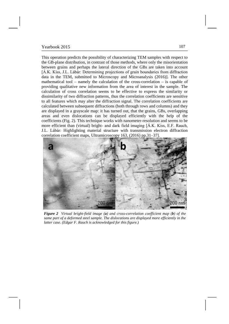
Yearbook 2015
107
This operation predicts the possibility of characterizing TEM samples with respect to
the GB-plane distribution, in contrast of those methods, where only the misorientation
between grains and perhaps the lateral direction of the GBs are taken into account
[Á.K. Kiss, J.L. Lábár: Determining projections of grain boundaries from diffraction
data in the TEM, submitted to Microscopy and Microanalysis (2016)]. The other
mathematical tool – namely the calculation of the cross-correlation – is capable of
providing qualitative new information from the area of interest in the sample. The
calculation of cross correlation seems to be effective to express the similarity or
dissimilarity of two diffraction patterns, thus the correlation coefficients are sensitive
to all features which may alter the diffraction signal. The correlation coefficients are
calculated between subsequent diffractions (both through rows and columns) and they
are displayed in a grayscale map: it has turned out, that the grains, GBs, overlapping
areas and even dislocations can be displayed efficiently with the help of the
coefficients (Fig. 2). This technique works with nanometer-resolution and seems to be
more efficient than (virtual) bright- and dark field imaging [Á.K. Kiss, E.F. Rauch,
J.L. Lábár: Highlighting material structure with transmission electron diffraction
correlation coefficient maps, Ultramicroscopy 163, (2016) pp.31–37].
Figure 2 Virtual bright-field image (a) and cross-correlation coefficient map (b) of the
same part of a deformed steel sample. The dislocations are displayed more efficiently in the
latter case. (Edgar F. Rauch is acknowledged for this figure.)

108
Nanobiosensorics „Lendület” Research Group
Head: Robert HORVÁTH, Ph.D., Senior Research Fellow
Research Staff
Robert HORVATH, Ph.D.
Sándor KURUNCZI, Ph.D.
Inna SZÉKÁCS, Ph.D.
Ph.D. students / Diploma workers
Norbert ORGOVÁN, Ph.D. student
Dániel PATKÓ, Ph.D. student
Beatrix PÉTER, Ph.D. student
András SAFTICS, Ph.D. student
Rita UNGAI-SALÁNKI, Ph.D.
student
Dávid CSIKAI, B.Sc. student
Enikő FORGÁCS, B.Sc. student
Gabriella GÁL, M.Sc. student
Aurél PRÓSZ, B. Sc. student
Barbara TÜRK, B.Sc. student
Ph.D. students / Diploma workers
Enikő FARKAS, M.Sc./Ph.D. student
Boglárka KOVÁCS, Ph.D. student
Judit NÁDOR, Ph.D. student
The Nanobiosensorics Group was established in 2012 in the framework of the
“Lendület” programme of the Hungarian Academy of Sciences. The “Lendület
programme” funds young researchers in Hungary aiming at the establishment of their
own independent research groups. The research profile of the Nanobiosensorics
Group is the development and application of label-free optical biosensors, the
mathematical modeling of the relevant biological and biophysical processes. Building
on their broad national and international collaborative network the group conducts
research in the fields of instrument development, monitoring of cell secreted
extracellular vesicles, development of protein-based functional coatings, adhesion
studies on human cancer and immune cells, and theoretical modeling.
In 2014, the application for an ERC Consolidator Grant by the head of the research
group received qualification category “A (fully meets the ERC excellence criteria and
should be funded if sufficient funds are available)” after the interview in Brussels, but
the funding line did not reach this proposal due to budgetary constraints. However,
using this achievement he could successfully apply for funding from NKFIH in the
framework of the ERC_HU call.

Yearbook 2015
109
Hydrogel film fabrication for biosensing
(Lendület Program, Bolyai Research Scholarship)
A. Saftics, S. Kurunczi, N.Q. Khánh, A. Sulyok, and R. Horváth
Hydrogel interface layers play an important role in the field of biosensors, especially
for label-free techniques. The 3D network of carbohydrate hydrogel dextran proved to
be advantageous for the enhanced immobilization capacity and for the reduced non-
specific binding of the sensor surface. We have been developing tailor-made
dextranized surfaces on different substrates.
Recently we have prepared carboxymethylated dextran (CMD) from native dextran in
our lab. Then this CMD (with Mw = 100 and 500 kDa) was used for ultrathin surface
coatings. Grafting methods based on covalent coupling to aminosilane- and
epoxysilane-functionalized surfaces were applied to obtain thin CMD layers. The
carboxyl moiety of the CMD was coupled to the aminated surface by EDC-NHS
reagents, while CMD coupling through epoxysilane molecules was performed
without any additional reagents. The surface layer investigation following the grafting
procedures included x-ray photoelectron spectroscopy (XPS), attenuated total
reflection infrared spectroscopy (ATR-IR), spectroscopic ellipsometry, atomic force
microscopy (AFM) and optical waveguide lightmode spectroscopy (OWLS). The in
situ OWLS method was suitable to devise the structure of the interfacial dextran
layers by the evaluation of the optogeometrical parameters. Our results suggested an
anisotropic layer that can be seen in Fig 1. The developed methodologies allowed to
design and fabricate nanometer scale ultrathin CMD layers with well-controlled
surface structure, which are very difficult to characterize in aqueous environments
using present instrumentation and highly hydrated surface layers.
Figure 1 Schematic illustrations
of the CMD grafting chemistries
and the supposed structure of the
CMD chains on the OWLS sensor
chip. The negative birefringence of
the layer suggested lain down
chains on the surface.
[A. Saftics, S. Kurunczi, Z. Szekrényes, K. Kamarás, N.Q. Khánh A. Sulyok, S.
Bősze, R. Horvath: Fabrication and characterization of ultrathin dextran layers: time
dependent nanostructure in aqueous environments revealed by OWLS, submitted
manuscript]

110
Label-free profiling of cell adhesion: Determination of the
dissociation constant for native cell membrane adhesion
receptor-ligand interaction
(“Lendület” grant LP2012-26/2012 of HAS)
N. Orgován, B. Péter, Sz. Bősze (ELTE, Budapest), Jeremy J. Ramsden (Cranfield University, UK), B. Szabó (ELTE, Budapest), and R. Horváth
Cellular adhesion is essential to life. Cells usually establish an anchorage with the
extracellular matrix or neighboring cells in the tissue using cell adhesion receptors
embedded in the cell membrane, such as integrins, cadherins, selectins, syndecans,
and the immunglobulin superfamily of adhesion receptors. Since nowadays many
modern drugs intervene at the level of cellular adhesion, there is an ever-increasing
demand for techniques that enable the effects of such drugs to be screened in a
straightforward and reliable way which moreover produce highly informative (e.g.,
multiparameter and/or kinetic) data.
Traditional methods for measuring cellular adhesion, including phase-contrast
microscopy or mechanical assays, where the adhered cells are subjected to a fluid
flow, are cumbersome and hence generally unsuitable for high throughput needed in
drug discovery, and kinetic monitoring with high temporal resolution and high signal-
to-noise ratio. In contrast, surface-sensitive label-free biosensors are inherently
capable of generating good-quality kinetic data. Evanescent field-based label-free
optical biosensors including resonant waveguide grating (RWG or Epic) biosensors
are considered to be especially straightforward means to monitor cell adhesion, since
they can in situ detect refractive index changes in the 100–200 nm thick layer closest
to the sensor surface, where the anchorage between the cell and its substratum takes
place. Moreover, the probing depth of these biosensors can be fine-tuned through
waveguide structure design, so dynamic information from various depths can be
simultaneously collected using multimode waveguides, potentially permitting the
monitoring of changes inside the cell or in its nucleus triggered by surface adhesion.
In this protocol we described how the adhesion kinetics of living cells on a surface
coated with integrin ligands can be characterized in detail. We use an optical
biosensor, an Epic BenchTop (BT) system to monitor cell adhesion with
unprecedented quality in a high-throughput way. The biosensor data recorded at
various ligand densities are used to determine the dissociation constant, so the binding
between the RGD ligand and its adhesion receptors embedded in their native cell
membrane is characterized in a label-free and perturbation-free manner (Fig. 1) . Of
note, the present protocol is equally applicable for other types of ligands and adhesion
receptors and can also be used to measure the effects of drugs interfering with cell
adhesion [Label-Free Biosensor Methods in Drug Discovery (Methods in
Pharmacology and Toxicology, 2015), Springer (Ed. Ye Fang), pp.233-252].

Yearbook 2015
111
Figure 1 Monitoring the adhesion kinetics of cells with an Epic biosensor on different
ligand densities enables the dissociation constant characterizing the interaction of native
cell membrane receptors and their ligands to be determined.
Incubator proof miniaturized Holomonitor to in situ monitor
cancer cells exposed to green tea polyphenol and preosteoblast
cells adhering on nanostructured titanate surfaces: validity of
the measured parameters and their corrections
(“Lendület” grant LP2012-26/2012 of HAS)
B. Péter, J. Nádor, K. Juhász, Á. Dobos, L. Kőrösi (Enviroinvest Ltd., Pécs, Hungary), I. Székács, D. Patkó, and R. Horváth
In 2015 we published two successful applications of holographic microscopy to
monitor cancer cell motility, migration, motility speed, and to examine the spreading
of preosteoblast cells on a nanostructured titanate coating [104]. The M4
Holomonitor, applied in this study, has a small size, and it is feasible to be put
directly into a humidified cell culture incubator. This technique is completely
noninvasive and label-free, therefore, nothing disturbs the cells during their
movements. A special mechanical stage was also developed in order to position the
sample into that range of the optical arrangement where digital autofocusing works
with high reproducibility and precision. With the help of this novel development, we
could perform two successful measurements demonstrating the capabilities of our
novel arrangement. In our first study, it is demonstrated that the movement of HeLa
cells was temperately reduced after the addition of polyphenol EGCg. This
phenomenon could be monitored in a completely noninvasive and label-free manner.

112
With this experiment, we proved that our recently developed sample stage is an
excellent tool for observing cell dynamical changes and monitoring the effects of
chemical substances on living cells. In another experiment, the Holomonitor M4 was
used to study cellular adhesion and spreading on nanostructured titanate coatings. A
novel arrangement was developed to measure live cell behavior on spin-coated
surfaces. We recorded the adhesion and spreading processes of the cells in real time.
From the recorded data, we concluded that the averaged cell thickness and area
detected by the instrument saturate after 30 min. These results are clearly
contradictive to previous investigations where the preosteoblast adhesion on these
nanostructured surfaces was monitored by an optical biosensor. Based on these
findings, we concluded that under certain thicknesses, relatively large parts of the
cells (parts of the thin lamellipodium) slick into the background surface due to the
limited vertical resolution of the optical arrangement (Fig. 2). We determined the
time-dependent corrected single-cell contact area and averaged thickness by the
assumption that the cell volume is constant during the adhesion process. Our new
correction method for estimation of the undetected parts of lamellipodia resulted in
more precise evaluations supported by earlier biosensor kinetic data [104].
Figure 1 (a): The detected and corrected data of the preosteoblast cells, (b): the area,
and (c): the thickness curves. Sometimes the lamellipodia, the very thin parts of the cells,
cannot be sensed perfectly by the instrument.

Yearbook 2015
113
Biophysical characteristics of proteins and living cells exposed
to the green tea polyphenol epigallocatecin-3-gallate (EGCg):
Review of recent advances from molecular mechanisms to
nanomedicine and clinical trials
(“Lendület” grant LP2012-26/2012 of HAS)
B. Péter, Sz. Bősze (ELTE, Budapest), and R. Horváth
Traditionally, tea was drunk to eliminate toxins, to improve blood flow and resistance
to diseases, so its habitual consumption has long been associated with health benefits.
Among natural compounds and traditional Chinese medicines, the green tea
polyphenol epigallocatechin gallate (EGCg) is one of the most studied active
substance. Tea catechins, especially (-)-EGCg, have been shown to have various
health benefits, for example anti-metastasis, anti-cardiovascular, anti-cancer, anti-
inflammatory and antioxidant effects (Fig. 1). In 2015 we focused on the molecular
Figure 1 Diversified effects of EGCg.
scale interactions between proteins and EGCg with special focus on its limited
stability and antioxidant properties, the observed biophysical effects of EGCg on

114
various cell lines and cultures. The alteration of cell adhesion, motility, migration,
stiffness, apoptosis, proliferation, as wells as the different impacts on normal and
cancer cells are all summarised in our prospective review article [Beatrix Péter,
Szilvia Bősze, Róbert Horváth: Biophysical characteristics of proteins and living cells
exposed to the green tea polyphenol epigallocatecin-3-gallate (EGCg): Review of
recent advances from molecular mechanisms to nanomedicine and clinical trials]. We
also handled the works performed using animal models, microbes and clinical trials.
Novel ways to develop its utilization as therapeutic purposes in the future are
discussed too, for instance, using nanoparticles and green tea polyphenols together to
cure illnesses, and the combination of EGCg and anticancer compounds to intensify
their effects. In this review we summarize the experiments and results of the past few
years. The limitations of the employed experimental models and the criticisms on the
interpretation of the obtained experimental data are summarized as well. We also
point out some inaccuracies in the literature.
Automated single cell isolation from suspension with computer
vision
(“Lendület” grant LP2012-26/2012 of HAS, Bolyai Scholarship, MedInProt)
R. Ungai-Salánki1,2,3, T. Gerecsei3, P. Fürjes4, N. Orgován2,3, N. Sándor5, E. Holczer4, R. Horváth2, and B. Szabó2,3,6
1Doctoral School of Molecular- and Nanotechnologies, PE, Veszprém, Hungary 2Nanobiosensorics Group, MTA EK MFA, Budapest, Hungary 3Department of Biological Physics, ELTE, Budapest, Hungary
4MEMS Laboratory, MTA EK MFA, Budapest, Hungary 5MTA-ELTE Immunology Research Group, Budapest, Hungary
6CellSorter Company for Innovations, Budapest, Hungary
Existing single cell isolation robots can manipulate only surface attached cells
seriously limiting the fields of their application for single cell handling. Although
naturally adherent cells can be spontaneously immobilized on the surface, the
adhesion force needs to be tuned either biochemically or by surface modifications
optimized to the cell type. Otherwise the too strongly adhered cells are picked up at
an expense of damaging the cell. We developed a computer vision-based robot
applying a motorized microscope and micropipette to recognize and gently isolate
intact individual cells for subsequent analysis, e.g., DNA/RNA sequencing in 1-2
nanolitres from suspension without immobilizing cells on the surface of the Petri dish
[R. Ungai-Salánki, T. Gerecsei, P. Fürjes, N. Orgován, N. Sándor, E. Holczer,
R. Horváth, B. Szabó: Automated single cell isolation from suspension with computer
vision, accepted for publication in Scientific Reports]. To minimize fluid convection
cells were kept in a thin (~100 µm) layer of buffer or culture medium covered by oil.
It can retrieve rare cells, needs minimal sample preparation, and can be applied for
virtually any tissue cell type. Combination of 1 µm positioning precision, adaptive

Yearbook 2015
115
cell targeting and below 1 nl liquid handling precision resulted in an unprecedented
accuracy and efficiency in robotic single cell isolation. We applied a 3D printer to
build miniature multi-well plates into the Petri dish. Single cells were injected either
into the wells of a miniature plate with a sorting speed of 3 cells/min or into standard
PCR tubes with 2 cells/min. We could isolate labeled cells also from dense cultures
containing ~1,000 times more unlabeled cells by the successive application of the
sorting process. We compared the efficiency of our method to that of single cell
entrapment in microwells and subsequent sorting with the automated micropipette:
the recovery rate of single cells was greatly improved. We expect that image-based
automated single cell manipulation will become an everyday technique of molecular
cell biology.
Figure 1 Automated micropipette for single cell isolation from a thin layer of suspension.
Panel a shows the concept of cell sorting. Cells are detected by computer vision. Cell
suspension confined into a thin ~100 µm layer of culture medium or buffer covered with
oil to avoid the convection-driven floating of cells. The glass micropipette with an inner
diameter of D= 30 µm approaches the surface of the dish to a distance of h= 5 µm.
Targeted cell is picked up by a slight vacuum connected to the micropipette and controlled
by a high speed fluid valve. Inhibitory effect of cell confinement into a thin layer on cell
floating is shown in b. Wells of the miniature plate (shown in c) printed into the Petri dish
further decreased convection.
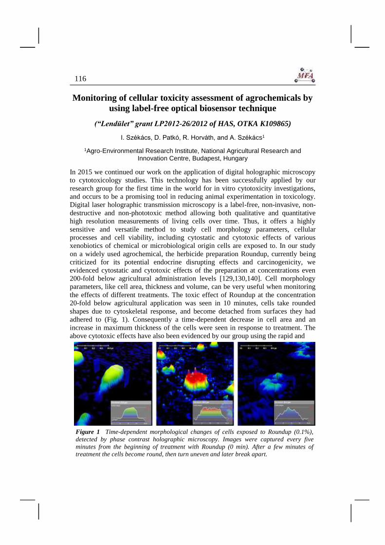
116
Monitoring of cellular toxicity assessment of agrochemicals by
using label-free optical biosensor technique
(“Lendület” grant LP2012-26/2012 of HAS, OTKA K109865)
I. Székács, D. Patkó, R. Horváth, and A. Székács1
1Agro-Environmental Research Institute, National Agricultural Research and Innovation Centre, Budapest, Hungary
In 2015 we continued our work on the application of digital holographic microscopy
to cytotoxicology studies. This technology has been successfully applied by our
research group for the first time in the world for in vitro cytotoxicity investigations,
and occurs to be a promising tool in reducing animal experimentation in toxicology.
Digital laser holographic transmission microscopy is a label-free, non-invasive, non-
destructive and non-phototoxic method allowing both qualitative and quantitative
high resolution measurements of living cells over time. Thus, it offers a highly
sensitive and versatile method to study cell morphology parameters, cellular
processes and cell viability, including cytostatic and cytotoxic effects of various
xenobiotics of chemical or microbiological origin cells are exposed to. In our study
on a widely used agrochemical, the herbicide preparation Roundup, currently being
criticized for its potential endocrine disrupting effects and carcinogenicity, we
evidenced cytostatic and cytotoxic effects of the preparation at concentrations even
200-fold below agricultural administration levels [129,130,140]. Cell morphology
parameters, like cell area, thickness and volume, can be very useful when monitoring
the effects of different treatments. The toxic effect of Roundup at the concentration
20-fold below agricultural application was seen in 10 minutes, cells take rounded
shapes due to cytoskeletal response, and become detached from surfaces they had
adhered to (Fig. 1). Consequently a time-dependent decrease in cell area and an
increase in maximum thickness of the cells were seen in response to treatment. The
above cytotoxic effects have also been evidenced by our group using the rapid and
Figure 1 Time-dependent morphological changes of cells exposed to Roundup (0.1%),
detected by phase contrast holographic microscopy. Images were captured every five
minutes from the beginning of treatment with Roundup (0 min). After a few minutes of
treatment the cells become round, then turn uneven and later break apart.

Yearbook 2015
117
high throughput optical biosensor technique, Epic BT. The main advantage of this
sensor is that it applies parallel multiple optical waveguide sensoric detection (e.g. on
384-well microplates) of given analytes or surface molecular processes using resonant
waveguide grating. This allows rapid parallel analysis of many samples. With the
Epic BT method we expand our study of Roundup, as well as its active ingredient
glyphosate and adjuvant polyethoxylated tallowamine (POEA) on preosteoblastic cell
line MC3T3-E1, as glyphosate has been indicated to inhibit bone development in rats.
The dynamics of living cell adhesion on nanostructured
genetically engineered molecular layers revealed by label-free
optical biosensors
("Lendület" grant LP2012-26/2012 of HAS, OTKA K104726)
B. Kovács, D. Patkó, I. Székács, N. Orgován, B. Tóth, F. Vonderviszt, and R. Horváth
Our purpose was to record the kinetics of cancer cell adhesion on layers of genetically
engineered protein variants, which are displaying cell adhesive RGD motifs. Wild
type protein coatings and synthetic polymer films were used in parallel control
experiments. We applied two types of waveguide sensors, optical waveguide light-
mode spectroscopy and Epic Benchtop system, to record cell adhesion on the surface.
The applied protein is a good target for genetic modifications. We constructed protein
variants which can display cell adhesive RGD motif. Specific cell surface receptors
(integrins) can recognize and bind these molecules, and trigger cell adhesion.
The experimental results confirmed that the PLL-g-PEG polymer coating prevents
cell adhesion, while the cells adhered and spread markedly on the RGD grafted PLL-
g-PEG polymer layer. On the layer of the wild type protein negligible adhesion could
be detected, contrary to the RGD displaying protein variants where significant cell
adhesion was observed (Fig. 1). Our work resulted in fine-tuned surface coatings for
basic cellular research and biomedical applications. It highlights the possibilities
offered by label-free technologies in cell biological research and development.
Figure 1 Schematic representation of anti-adhesive and adhesive surface coating induced
cell behavior. a: Wild type protein surface coating hinders cell adhesion on the sensor
surface. b: RGD displaying protein surface coating induces cell adhesion and spreading.

118
Complex Systems Department
Head: György SZABÓ, D.Sc., scientific advisor
Research Staff
István BORSOS
Imre EÖRDÖGH
Zoltán JUHÁSZ, Ph.D.
Géza ÓDOR, Ph.D.
Károly SZÁSZ, engineer
Attila SZOLNOKI, D.Sc.
Ph.D. students / Diploma workers
Levente VARGA, Ph.D. student
Balázs KIRÁLY, Ph.D. student
Kristóf HÓDSÁGI, student
The main field of research of the Complex Systems group is the statistical physical
analysis of non-equilibrium systems mostly centred around many-agent evolutionary
game theoretic models, like investigating processes maintaining honest behaviour,
e.g. the effects of punishment, evolutionary dynamics and interconnection on the
level of cooperation. Among the innovations is the introduction of individual
differences causing the players to „re-evaluate” their income, e.g. by amplifying the
acceptance of the neighbour’s opinion. Another topic is the role of cyclic interactions
supporting the maintenance of multi-strategy states (biodiversity) in spatial models.
We have studied the decomposition of symmetric matrix games into four elementary
interactions. The coordination games have been extended by additional neutral
strategies preserving the order-disorder phase transition when the noise is increased,
which is characteristic of the Ising models.
The statistical physical investigation of dynamic processes on random graphs can be
materially used in brain research and in the interpretation of social and biological
phenomena. This emphasises the study of slow processes (Griffiths phase) on
hierarchic and modular networks. Our numerical investigations showed power-law
behaviour, which is typical of critical transitions in interconnection systems
characteristic of the neural cells of the brain. We have continued the numerical
investigation of surface growth in cooperation with German researchers.
Earlier analysis of folk music has been continued and connected to numerical analysis
of genetic and linguistic relatedness. The distribution of haplogroups inherited
matrilineally has been studied together with geneticists. Our experts have participated
in the R&D project ”Introducing cognitive methods to improve protection against
vehicle collisions”, using their experience in software development for image
processing.
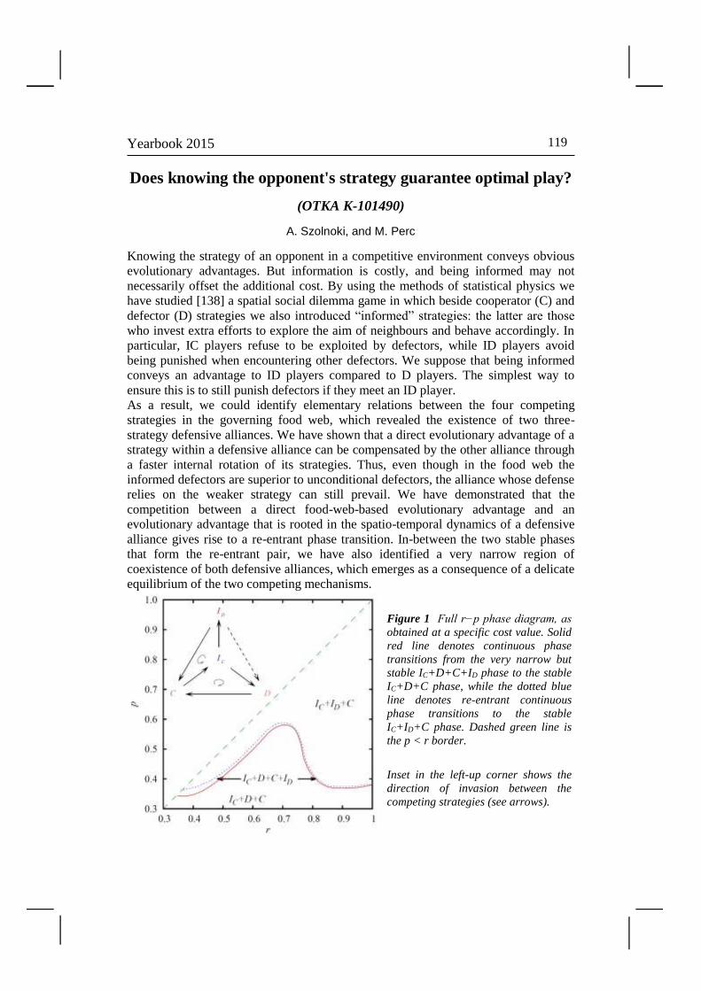
Yearbook 2015
119
Does knowing the opponent's strategy guarantee optimal play?
(OTKA K-101490)
A. Szolnoki, and M. Perc
Knowing the strategy of an opponent in a competitive environment conveys obvious
evolutionary advantages. But information is costly, and being informed may not
necessarily offset the additional cost. By using the methods of statistical physics we
have studied [138] a spatial social dilemma game in which beside cooperator (C) and
defector (D) strategies we also introduced “informed” strategies: the latter are those
who invest extra efforts to explore the aim of neighbours and behave accordingly. In
particular, IC players refuse to be exploited by defectors, while ID players avoid
being punished when encountering other defectors. We suppose that being informed
conveys an advantage to ID players compared to D players. The simplest way to
ensure this is to still punish defectors if they meet an ID player.
As a result, we could identify elementary relations between the four competing
strategies in the governing food web, which revealed the existence of two three-
strategy defensive alliances. We have shown that a direct evolutionary advantage of a
strategy within a defensive alliance can be compensated by the other alliance through
a faster internal rotation of its strategies. Thus, even though in the food web the
informed defectors are superior to unconditional defectors, the alliance whose defense
relies on the weaker strategy can still prevail. We have demonstrated that the
competition between a direct food-web-based evolutionary advantage and an
evolutionary advantage that is rooted in the spatio-temporal dynamics of a defensive
alliance gives rise to a re-entrant phase transition. In-between the two stable phases
that form the re-entrant pair, we have also identified a very narrow region of
coexistence of both defensive alliances, which emerges as a consequence of a delicate
equilibrium of the two competing mechanisms.
Figure 1 Full r−p phase diagram, as
obtained at a specific cost value. Solid
red line denotes continuous phase
transitions from the very narrow but
stable IC+D+C+ID phase to the stable
IC+D+C phase, while the dotted blue
line denotes re-entrant continuous
phase transitions to the stable
IC+ID+C phase. Dashed green line is
the p < r border.
Inset in the left-up corner shows the
direction of invasion between the
competing strategies (see arrows).

120
Figure 2 Snapshots of pattern formation, as obtained for r = 0.65 (top row) and r = 0.95
(bottom row) starting from a prepared initial state. During the relaxation period, each half
of the lattice contained the strategies of one triplet only. After the characteristic patterns
evolved (leftmost panels), the separating white wall was removed and the two defensive
alliances started to compete with each other. In the top row, the (IC+D+C) triplet ( dark
blue, light blue, and light red, overall lighter), gradually compresses the (IC +ID+C) triplet
(dark blue, light blue, and dark red, overall darker). The typical size of the shrinking
alliance is encircled with a white ellipse. The snapshots were taken after different iteration
steps from left to right. In the bottom row, the (IC+ID+C) triplet gradually gets dominant
because ID players are superior to D players. Accordingly, the domains of the (IC+D+C)
triplet (white ellipses) vanish over time.
Eurasian mtDNA analysis with a new iterative rank-
correlation method
(OTKA K-81954)
Z. Juhász, T. Fehér, E. Németh, and H. Pamjav
We have analysed 27-dimensional mtDNA haplogroup distributions of 174 Eurasian,
North-African and American populations to describe the haplogroup distributions of
populations as composites of certain hypothetic ancient core populations immediately
or indirectly determining the migration processes in Eurasia [58]. To identify these
core populations, a new iterative algorithm determines the clusters of the 27 studied
haplogroups having strong rank-correlations. Combined with our Self Organising
Cloud algorithm this allowed us to determine geographically, historically and
linguistically interpretable clusters of our dataset having a very specific structure
defying classification. Figure 1 shows the rank correlations, where the distances
driving the MDS algorithm were calculated as 1-rank correlation for all pairs of Hg-s.
Three disjoint “correlating haplogroup clusters” (CHgC) are clearly identified:

Yearbook 2015
121
Figure 1 MDS graph of the correlations
between 27 MTDNA haplogroups in
Eurasia an America. Thin and thick edges
indicate correlations over 0.67 and 0.74
respectively.
Figure 2 The main haplogroup
distribution of a composite cluster
obtained by the Self Organising
Cloud algorithm (a), and the
location of the related populations
in the general MDS-map of the
174 Hg distributions (b).
Siberian, Western and Eastern
components are denoted by black,
grey and white columns. Ancient
Bronze-age distributions of the
Andronovo culture are BBA
(Baraba Steppe), LKR (Late
Krotovo), UST (Ustinovo), FYO
(Fyodorovo). Recent descendants
– UYG (Uygur), UZB (Uzbek),
KOP (Komi), TUR (Turkish), SEK
(Székely), TAT (Tatar), MRI
(Mari), MRD (Mordvin) are
mainly Uralic and Altaic speaking
populations.
The relatively large number of ancient DNA samples provided an invaluable tool for
comparing ancient population movements with the location of living populations.
Comparing the ancient data of the Andronovo and the Kurgans areas to recent
distributions led us to conclude that current East and Central European populations
may consist of a Western substrate arising from the Near Eastern Neolithic stock and
a Siberian-Western composite population arising from the Andronovo area. The close
relations of recent and ancient haplogroup distributions of these areas also make it
probable that Uralic and Altaic languages could have played a significant maternal
role in the Andronovo culture, and Uralic-speakers in the Kurgans culture.
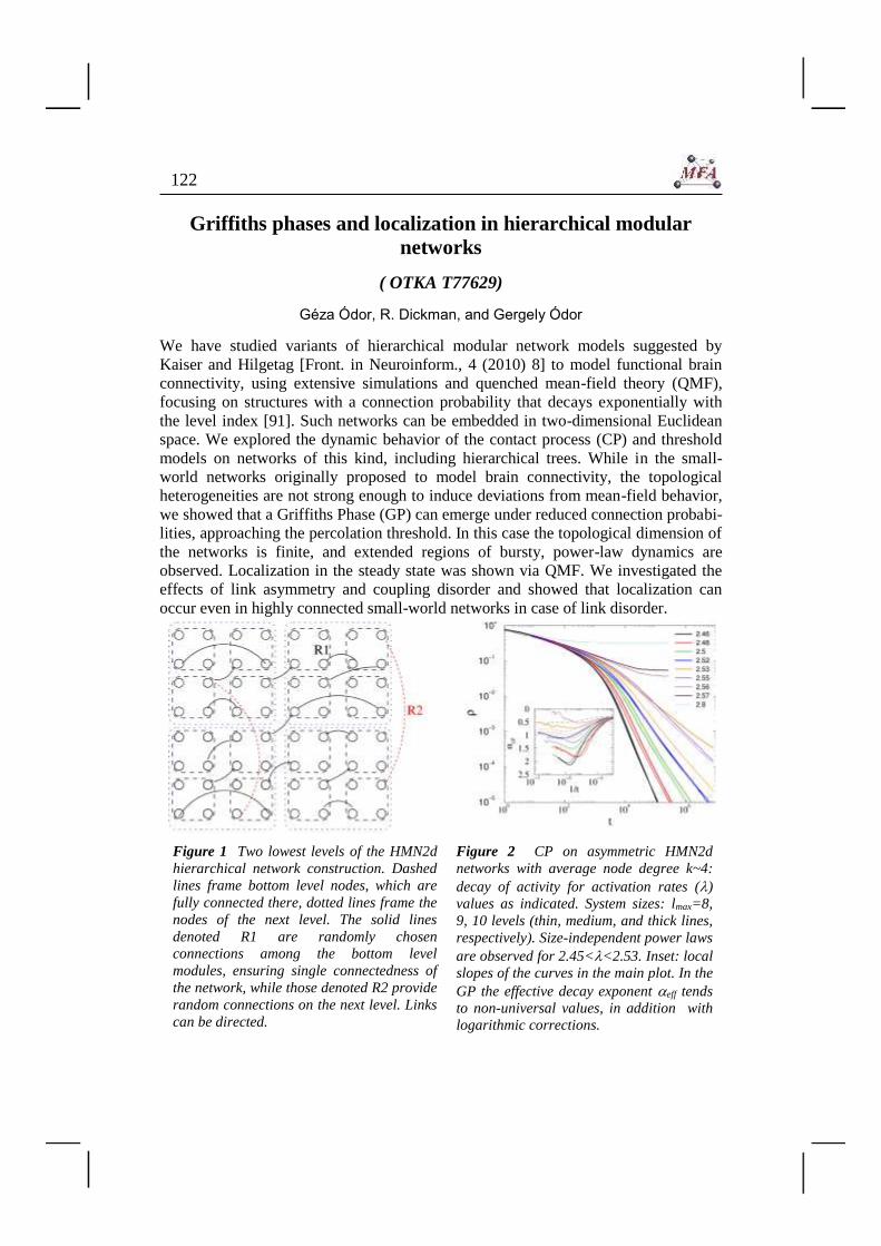
122
Griffiths phases and localization in hierarchical modular
networks
( OTKA T77629)
Géza Ódor, R. Dickman, and Gergely Ódor
We have studied variants of hierarchical modular network models suggested by
Kaiser and Hilgetag [Front. in Neuroinform., 4 (2010) 8] to model functional brain
connectivity, using extensive simulations and quenched mean-field theory (QMF),
focusing on structures with a connection probability that decays exponentially with
the level index [91]. Such networks can be embedded in two-dimensional Euclidean
space. We explored the dynamic behavior of the contact process (CP) and threshold
models on networks of this kind, including hierarchical trees. While in the small-
world networks originally proposed to model brain connectivity, the topological
heterogeneities are not strong enough to induce deviations from mean-field behavior,
we showed that a Griffiths Phase (GP) can emerge under reduced connection probabi-
lities, approaching the percolation threshold. In this case the topological dimension of
the networks is finite, and extended regions of bursty, power-law dynamics are
observed. Localization in the steady state was shown via QMF. We investigated the
effects of link asymmetry and coupling disorder and showed that localization can
occur even in highly connected small-world networks in case of link disorder.
Figure 1 Two lowest levels of the HMN2d
hierarchical network construction. Dashed
lines frame bottom level nodes, which are
fully connected there, dotted lines frame the
nodes of the next level. The solid lines
denoted R1 are randomly chosen
connections among the bottom level
modules, ensuring single connectedness of
the network, while those denoted R2 provide
random connections on the next level. Links
can be directed.
Figure 2 CP on asymmetric HMN2d
networks with average node degree k~4:
decay of activity for activation rates ()
values as indicated. System sizes: lmax=8,
9, 10 levels (thin, medium, and thick lines,
respectively). Size-independent power laws
are observed for 2.45<<2.53. Inset: local
slopes of the curves in the main plot. In the
GP the effective decay exponent eff tends
to non-universal values, in addition with
logarithmic corrections.

Yearbook 2015
123
MFA Seminar Talks
2015.01.07 Gergely MÁRTON (Semmelweis University, Budapest, Hungary): “Development
and characterisation of novel microelectrode arrays for
neurophysiology”
2015.02.28 Zoltán HAJNAL (MTA EK MFA, Budapest, Hungary): “Közelítő módszerek az
atomi és molekuláris modellezésben”
2015.02.04 Dániel PATKÓ (MTA EK MFA, Budapest, Hungary): “Nagyérzékenységű
jelölésmentes bioszenzorika”
2015.03.05 Péter VANCSÓ (MTA EK MFA, Budapest, Hungary): “Töltésterjedés grafén
nanoszerkezetekben”
2015.03.31 Carl FRANCK (Cornell University, USA): “Surprises in Unicellular Eucariotic
Sensing”
2015.05.06 MTA közgyűlés
2015.05.13 Béla PÉCZ (MTA EK MFA, Budapest, Hungary): “GaN heterostructures
with diamond and graphene for high power applications”
2015.05.20 Aryasomayajulu SUBRAHMANYAM (ITT Madras, Chennai, India): “Hospital Acquired Infection
(HAI): what can be done by a material scientist?”
2015.05.27 Sándor KUGLER (BME, Physics Institute, Budapest, Hungary): “Fascinating
amorphous semiconductors”
2015.06.03 Péter BARNA (MTA EK MFA, Budapest, Hungary): “A vékonyrétegkutatás
koncepciója 60 év távlatából”
2015.06.10 György Zoltán RADNÓCZI (MTA EK MFA, Budapest, Hungary): “Amorf Si Ni indukálta
kristáyosodása”
124
2015.06.17 Peter LOBOTKA (ELU SAV, Bratislava, Slovakia): “Fabrication of metallic
nanoparticles in ionic liquid”
2015.08.31-
-2015.09.01 Nobuo TANAKA
(EcoTopia Science Institute, Nagoya University, Japan):
“HREM - 2-days seminar/course”
2015.10.14 Zsolt Endre HORVÁTH (MTA EK MFA, Budapest, Hungary): “Vezető polimer
kompozitok”
2015.10.21 Miklós KELLERMAYER (Semmelweis University, Budapest, Hungary): “Modern
mikroszkópos eljárások egyedi molekulák vizsgálatára”
2015.10.28 Nikolett OLÁH (MTA EK MFA, Budapest, Hungary): “Bioinert Ti-C
nanokompozit fejlesztése orvosi implantátumok felületi tulajdon-
ságainak javítása céljából”
2015.11.05 Hiroshi AMANO (Nagoya University, Japan): “Progress in III-nitride
nanodevices”
2015.11.11 Szabolcs CSONKA (BME, Budapest, Hungary): “Kvantum dotok felfüggesztett
grafénban”
2015.11.18 Pavel B. SOROKIN (Russia): “New specific properties of 2D films”
2015.12.02 Ákos Koppány KISS (MTA EK MFA, Budapest, Hungary): “Szemcsehatárok
transzmissziós elektronmikroszkópos vizsgálati módszereinek
fejlesztése”
2015.12.08 Peter SAMUELY
(UEF SAV, Kosice, Slovakia): “The Kosice Centre of Low
Temperature Physics”
2015.12.08 Pavol SZABÓ
(UEF SAV, Kosice, Slovakia): “Superconductivity near
transition to insulating state in molybdenum carbide”

Yearbook 2015
125
Research and Development Partners, Foreign Visitors
AMANO, Hiroshi (Nagoya University, Japan)
ANTIPINA, Liubov Yu. (Russia)
ARAKAWA, Hanae (Japan)
ASLAMACI, Abdullah (INOVENSO Ltd., Turkey)
BENES, Roman (Anton Paar, Graz, Austria)
BEREKMÉRI, Evelin (Romania)
BEROZ, Masud (ComponentZEE LLC , USA)
BOSI, Matteo (IMEM-CNR, Parma, Italy)
BREUER, Stefan (Technische Universität Darmstadt, Germany)
BRUNO, Friedhelm (Germany)
CARBONI, Alberto (Italy)
CHAPELIER, Claude (France)
COTTIER, Kaspar (Creoptix GmbH, Wädenswil, Switzerland)
CSIKAI Dávid (Romania)
DARMIL, Guillaume (France)
DAS, Partha Pratim (India)
DING, Zejun (China)
DRAGANITS, Gerhard (Zeiss, Austria)
FARBER, Paul (Robert Bosch Kft., Germany)
FIEDLER, Christian (Agilent, Germany)
FRANK, Carl Peter (USA)
GASTNER, Michael Thorsten (Germany)
GILMORE, Mark (UK)
HERBERT, Damnik Niklas (Germany)
HUNT, Steven (FEI, UK)
HWANG Chanyong (Korean Research Institute of Standards and Science, Daejon,
South Korea)
ISHIHARA, Sotomi (Toyama National College, Toyama, Japan)
KAENDERS, Wilhelm (Toptica AG, Germany)
KELLING, Jeffrey (HZDR, Dresden, Germany)
KOMÁN Zsolt (Romania)
KUMAR, Srivastawa Pawan (India)
KUNZO, Pavol (ELU SAV, Slovakia)
KUROKAWA, K. (Tateyama Kagaku, Japan)
LATHUS, Guillaume (France)
LOBOTKA, Peter (ELU SAV, Bratislava, Slovakia)
MANGANIELLO, Adam (USA)
MANUSCO, James F. (USA)
McWILLIAMS, Christopher John (UK)
NAGY Ádám (Slovakia)
NAWRAT, Zbigniew (Poland)
NAZIRIZADEH, Yousef (Germany)

126
NÉMET Anikó (Serbia)
NERGAARD, Per Olav (Norway)
NEWMAN, David (UK)
NUTSCH, Andreas (Fraunhofer IISB, Germany)
O'DONNELL, James (France)
ORBÁN Szabolcs (Romania)
ORBÁNOVÁ, Ágnesa (Slovakia)
PINTO, Fabrizio (USA)
RAMSDEN, Jeremy (UK)
ROHR, Kamil (Poland)
SCHATZ, Oliver (Robert Bosch Kft., Germany)
SCHÖNENBERGER, Christian (Switzerland)
SOROKIN, Pavel B. (Russia)
SPIGA, Fabio (Italy)
STEINRÜCK, Hans-Peter (Germany)
SUBRAHMANYAM, Aryasomayajulu (ITT Madras, Chennai, India)
SZABÓ, Pavol (UEF SAV, Slovakia)
TADA, Kazihuro (National Institute for Technology, Toyama, Japan)
TAKAGI, Toshiyuki (Tohoku University, Sendai, Japan)
TANAKA, Nobuo (EcoTopia Science Institute, Nagoya University, Japan)
TERAYAMA, H. (Tateyama Kagaku, Japan)
TRIVUN, Dusko (Bosnia and Hercegovina)
UZUNER, Talha (INOVENSO Ltd., Turkey)
VANAJA, Aryasomayajula (India)
VARGA Levente (Romania)
VÁVRA, Jan (JPK Instruments AG, Checz Republik)
WATANUKI, Osamu (Tateyama Kagaku, Japan)
XU, Huan (China)

Yearbook 2015
127
MFA Publications in 2015 1. Agócs E, Bodermann B, Burger S, Dai G, Endres J, Hansen PE, Nielsen L, Madsen MH,
Heidenreich S, Krumrey M, Loechel B, Probst J, Scholze F, Soltwisch V, Wurm M:
"Scatterometry reference standards to improve tool matching and traceability in
lithographical nanomanufacturing", Progress in Biomedical Optics and Imaging (Proc of
SPIE) 9556: Paper 955610, p.12 (2015), DOI:10.1117/12.2190409
2. Albert E, Albouy PA, Ayral A, Basa P, Csík G, Nagy N, Roualdés S, Rouessac V, Sáfrán
G, Suhajda Á, Zolnai Zs, Hórvölgyi Z: "Antibacterial properties of Ag-TiO2 composite sol-
gel coatings", RSC Advances 5:(73) pp.59070-59081 p.11 (2015)
3. Albert E, Basa P, Deák A, Németh Á, Osváth Z, Sáfrán G, Zolnai Zs, Hórvölgyi Z, Nagy
N: "Introducing nanoscaled surface morphology and percolation barrier network into
mesoporous silica coatings", RSC Advances 5:(74) pp.60041-60053 (2015)
4. Albert E, Cotolan N, Nagy N, Sáfrán G, Szabó G, Mureşan LM, Hórvölgyi Z:
"Mesoporous silica coatings with improved corrosion protection properties", Microporous
and Mesoporous Materials 206 pp.102-113 (2015)
5. An H, Wang J, Szívós J, Harumoto T, Sannomiya T, Muraishi S, Sáfrán G, Nakamura Y,
Shi J: "Perpendicular coercivity enhancement of CoPt/TiN films by nitrogen incorporation
during deposition", J Appl Phys 118:(20) Paper 203907 p.4 (2015)
6. Anaya J, Rossi S, Alomari M, Kohn E, Tóth L, Pécz B, Kuball M: "Thermal conductivity of
ultrathin nano-crystalline diamond films determined by Raman thermography assisted by
silicon nanowires", Appl Phys Lett 106:(22) Paper 223101 p.5 (2015)
7. Anooz BS, Petrik P, Schmidbauer M, Remmele T, Schwarzkopf J: "Refractive index and
interband transitions in strain modified NaNbO3 thin films grown by MOCVD", J Physics D
- Applied Physics 48:(38) Paper 385303 p.9 (2015)
8. Babenko V, Murdock AT, Koós AA, Britton J, Crossley A, Holdway P, Moffat J, Huang J,
Alexander-Webber JA, Nicholas RJ, Grobert N: "Rapid epitaxy-free graphene synthesis
on silicidated polycrystalline platinum", Nature Communications 6: Paper 7536 p.8 (2015)
9. Balázsi Cs, Tapasztó O, Balázsi K: "Structural Investigation of Biogenic Calcium
Phosphate Based Composites Prepared by Electrospinning", In: Ágnes Kittel, Pécz B
(Eds.), 12th Multinational Congress on Microscopy: MCM 2015., Eger, Hungary,
20150823-28, Budapest: Akadémiai Kiadó, pp.523-524 (2015)
10. Balázsi K, Balázsi Cs: "Biogenic Hydroxyapatite Based Implant Materials", In: Thakur
VK, Kessler MR (Eds.), Green Biorenewable Biocomposites: From Knowledge to
Industrial Applications, Waretown: Apple Academic Press Ltd., pp.27-57 (2015)
11. Balázsi K, Barkóczy P, Bársony I, Czvikovszky T, Gyulai J, Hohol R, Janó V, Kaptay Gy,
Kocsis-Baán M, Kónya I, Kuzsella L, Lendvai J, Szabó PJ, Tóth Lá, Verő B, Zsámbók D
(Eds.): Országos Anyagtudományi Konferenciasorozat 1997-2015, Jubileumi Kiadvány:
Anyagtudomány, anyagvizsgálat, anyaginformatika, Balatonalmádi, Hungary, 20151011-
13, Budapest: Magyar Anyagtudományi Egyesület, (2015), (ISBN:978-963-12-3494-7)
12. Balázsi K: "Hypoallergenic Ceramic Implant Materials: Preparation and Properties", In:
Ágnes Kittel, Pécz B (Eds.), 12th Multinational Congress on Microscopy: MCM 2015,
Eger, Hungary, 20150823-28, Budapest: Akadémiai Kiadó, pp.137-139 (2015)

128
13. Barna PB: "Pócza tanár úr - születésének 100. évfordulóján", Fizikai Szemle 65:(11)
pp.372-376 (2015)
14. Bársony I: "A céltudatosság jutalma (A 2014-es fizikai Nobel-díjról)", Fizikai Szemle
65:(1) pp.33-35 (2015)
15. Bársony I: "Paradigmaváltás az ezredforduló anyagkutatásában", In: Balázsi K,
Barkóczy P, Bársony I, Czvikovszky T, Gyulai J, Hohol R, Janó V, Kaptay Gy, Kocsis-
Baán M, Kónya I, Kuzsella L, Lendvai J, Szabó PJ, Tóth Lá, Verő B, Zsámbók D (Eds.),
Országos Anyagtudományi Konferenciasorozat 1997-2015, Jubileumi Kiadvány:
Anyagtudomány, anyagvizsgálat, anyaginformatika, Balatonalmádi, Hungary, 20151011-
13, Budapest: Magyar Anyagtudományi Egyesület, pp.124-133 (2015), (ISBN:978-963-
12-3494-7)
16. Battistig G: "Introduction: REM7 - 2014", Radiation Effects and Defects in Solids 170:(3)
pp.153-154 (2015)
17. Beke D, Szekrényes Zs, Czigány Zs, Kamarás K, Gali Ádám: "Dominant luminescence is
not due to quantum confinement in molecular-sized silicon carbide nanocrystals",
Nanoscale 7:(25) pp.10982-10988 (2015)
18. Bódis E, Tapasztó O, Zoltán K, Fazekas P, Klébert Sz, Keszler AM, Balázsi K,
Szépvölgyi J: "Spark plasma sintering of Si3N4/multilayer graphene composites", Open
Chemistry 13:(1) pp.484-489 (2015)
19. Bohner B, Schuszter G, Nakanishi H, Zámbó D, Deák A, Horváth D, Tóth Á, Lagzi I:
"Self-Assembly of Charged Nanoparticles by an Autocatalytic Reaction Front", Langmuir
31:(44) pp.12019-12024 (2015)
20. Bulusheva LG, Okotrub AV, Fedoseeva YuV, Kurenya AG, Asanov IP, Vilkov OY, Koós
AA, Grobert N: "Controlling pyridinic, pyrrolic, graphitic, and molecular nitrogen in multi-
wall carbon nanotubes using precursors with different N/C ratios in aerosol assisted
chemical vapor deposition", Physical Chemistry Chemical Physics 17:(37) pp.23741-
23747 (2015)
21. Chandrappan J, Murray M, Kakkar T, Petrik P, Agócs E, Zolnai Zs, Steenson DP, Jha A,
Jose G: "Target dependent femtosecond laser plasma implantation dynamics in enabling
silica for high density erbium doping", Scientific Reports 5: Paper 14037 p.8 (2015)
22. Chandrappan J, Murray M, Petrik P, Agócs E, Zolnai Zs, Tempez A, Legendre S,
Steenson DP, Jha A, Jose G: "Doping silica beyond limits with laser plasma for active
photonic materials", Optical Materials Express 5:(12) pp.2849-2861 p.12 (2015)
23. Chen X, Szolnoki A, Perc M: "Competition and cooperation among different punishing
strategies in the spatial public goods game", Phys Rev E Stat Nonlin 92:(1) Paper 012819
p.6 (2015)
24. Chubarov M, Pedersen H, Högberg H, Czigány Zs, Garbrecht M, Henry A: "Polytype
pure sp2-BN thin films as dictated by the substrate crystal structure", Chemistry of
Materials 27:(5) pp.1640-1645 p.6 (2015)
25. Chubarov M, Pedersen H, Högberg H, Garbrecht M, Czigány Zs, Andersson SG, Henry
A: "Chemical Vapor Deposition of Boron Nitride Thin Films on SiC", Materials Science
Forum 821-823: pp.990-994 (2015)
26. Chubarov M, Pedersen H, Högberg H, Henry A, Czigány Zs: "Initial stages of growth and
the influence of temperature during chemical vapor deposition of sp2-BN films", J

Yearbook 2015
129
Vacuum Science and Technology A-Vacuum Surfaces and Films 33:(6) Paper 061520
p.6 (2015)
27. Cora I, Dódony I, Tóth L, Kiss KÁ: "Study of Si-containing pyrite (FeS2)", In: Ágnes Kittel,
Pécz B (Eds.), 12th Multinational Congress on Microscopy: MCM 2015, Eger, Hungary,
20150823-28, Budapest: Akadémiai Kiadó, pp.275-276, p.2 (ISBN:978-963-05-9653-4)
(2015)
28. Cota WFC, Ferreira SC, Ódor G: "Griffiths effects of the susceptible-infected-susceptible
epidemic model on random power-law networks", (2015), arXiv:1512.05274
29. Craciun D, Socol G, Cristea DV, Stoicanescu M, Olah N, Balazs K, Stefan N, Lambers E,
Craciun V: "Mechanical properties of pulsed laser deposited nanocrystalline SiC films",
Appl Surf Sci 336: pp.391-395. (2015)
30. Daróczi CsS (Eds.): "MTA EK MFA Yearbook 2014", Budapest: MTA MFA, 2015. 144p.
(2015)
31. Datz D, Gasparics A, Vértesy G: "Study of the Fluxset Magnetic Probe Speed-Sensitivity
Developed for Detection of Magnetic Nanoparticles in Surgery", J Electrical Eng 66:(1)
pp.57-60 (2015)
32. Deschler F, Riedel D, Deák A, Ecker B, Hauff EV, Como ED: "Imaging of morphological
changes and phase segregation in doped polymeric semiconductors", Synthetic Metals
199: pp.381-387 (2015)
33. Dillon FC, Moghal J, Koós AA, Lozano JG, Miranda L, Porwal H, Reece MJ, Grobert N:
"Ceramic composites from mesoporous silica coated multi-wall carbon nanotubes",
Microporous and Mesoporous Materials 217: pp.159-166 (2015)
34. Dobrik G: "Szén alapú nanoarchitektúrák kialakítása és jellemzése pásztázószondás
módszerekkel", 127p. (PhD) (2015)
35. Dódony E, Radnóczi GyZ, Pécz B, Stoemenos J, Vouroutzis N, Frangis N: "Investigating
MILC Processes in Extreme Conditions", In: Ágnes Kittel, Pécz B (Eds.), 12th
Multinational Congress on Microscopy: MCM 2015., Eger, Hungary, 20150823-28,
Budapest: Akadémiai Kiadó, pp.250-252 (2015)
36. Fekete B, Kasl J, Jandova D, Jóni B, Trampus P, Misják F: "Low cycle thermomechanical
fatigue of reactor steels: microstructural and fractographic", Materials Science and
Engineering: A Publication of the University of Miskolc 640: pp.357-374 (2015)
37. Fekete Z, Németh A, Márton G, Ulbert I, Pongrácz A: "Experimental study on the
mechanical interaction between silicon neural microprobes and rat dura mater during
insertion", J Mater Sci-Materials Medicine 26:(2) Paper 70 p.21 (2015)
38. Fekete Z: "Recent advances in silicon-based neural microelectrodes and microsystems:
a review", Sensors Actuators B Chemical 215: pp.300-315 (2015)
39. Fekete Z: "Technology of ultralong deep brain fluidic microelectrodes combined with
etching-before-grinding", Microsystem Technologies 21:(2) pp.341-344 (2015)
40. Fogarassy Zs: "Fizikai és kémiai módszerekkel gőzfázisból leválasztott szerkezetek
kialakítása és jellemzése", 117p. (PhD) (2015)
41. Fried M, Major Cs, Juhász Gy, Petrik P, Horváth Z: "Expanded beam speetro-
ellipsometry for big area on-line monitoring", Proc of SPIE - Int Soc Optical Eng 9525:
Paper 95251S p.12 (2015)

130
42. Frigeri C, Serényi M, Szekrényes Z, Kamarás K, Csik A, Khánh NQ: "Effect of heat
treatments on the properties of hydrogenated amorphous silicon for PV and PVT
applications", Solar Energy 119: pp.225-232 (2015)
43. Fürjes P, Holczer EG, Tóth E, Iván K, Fekete Z, Bernier D, Dortu F, Giannone D: "PDMS
microfluidics developed for polymer based photonic biosensors", Microsystem
Technologies 21:(3) pp.581-590 (2015)
44. Galkin NG, Galkin KN, Goroshko DL, Chernev IM, Shevlyagin AV, Dózsa L, Osváth Z,
Pécz B: "Non-doped and doped Mg stannide films on Si(111) substrates: Formation,
optical, and electrical properties", Jap J Appl Phys 54:(7) Paper 07JC06 p.9 (2015)
45. Galkin NG, Goroshko DL, Galkin KN, Shevlyagin A, Chernev IM, Maslov AM, Dotsenko
SA, Subbotin EY, Dózsa L, Osváth Z, Pécz B, Kudrawiec R, Misiewicz J:
"Semiconducting Mg2Sn and Mg2Ge nanolayers on Si(111) substrates: formation,
structure and properties", In: V E Borisenko, S V Gaponenko, V S Gurin, C H Kam (Eds.),
Physics, Chemistry and Applications of Nanostructures: Proc Int Conference
Nanomeeting, Minsk, Belorussia, 20150526-29, Minsk: World Scientific, pp.128-131
(2015)
46. Gastner MT, Ódor G: "The topology of large Open Connectome networks for the human
brain", (2015), arXiv:1512.01197
47. Gergely-Fülöp E, Nagy N, Deák A: "Langmuir-Blodgett films of gold nanorods with
different silica shell thicknesses", Period Polytechn Chem Eng 59:(2) pp.104-110 Paper
7596 (2015)
48. Gergelyi D, Földesy P, Zarándy Á: "Scalable, Low-Noise Architecture for Integrated
Terahertz Imagers", J Infrared Millimeter and Terahertz Waves 36:(6) pp.520-536 p.17
(2015)
49. Goroshko D, Chusovitin E, Bezbabniy D, Dózsa L, Pécz B, Galkin N: "Formation and
Thermoelectric Properties of Si/CrSi2/Si(001) Heterostructures with Stressed Chromium
Disilicide Nanocrystallites", Electronic Materials Letters 11:(3) pp.424-428 (2015)
50. Gubicza J, Hegedűs Z, Lábár JL, Kauffmann A, Freudenberger J, Sarma VS: "Solute
redistribution during annealing of a cold rolled Cu-Ag alloy", J Alloys and Compounds
623: pp.96-103 (2015)
51. Gurbán S, Kotis L, Pongrácz A, Sulyok A, Tóth AL, E Vázsonyi, Menyhárd M: "The
chemical resistance of nano-sized SiC rich composite coating", Surface and Coatings
Technology 261: pp.195-200 (2015)
52. Gyulai J: "Funkcionális anyagok - 2000 +15+...", In: Balázsi K, Barkóczy P, Bársony I,
Czvikovszky T, Gyulai J, Hohol R, Janó V, Kaptay Gy, Kocsis-Baán M, Kónya I, Kuzsella
L, Lendvai J, Szabó PJ, Tóth Lá, Verő B, Zsámbók D (Eds.), Országos Anyagtudományi
Konferenciasorozat 1997-2015, Jubileumi Kiadvány: Anyagtudomány, anyagvizsgálat,
anyaginformatika, Balatonalmádi, Hungary, 20151011-13, Budapest: Magyar
Anyagtudományi Egyesület, pp.116-123 (2015), (ISBN:978-963-12-3494-7)
53. Horváth R, Gardener H, Ramsden J: "Apparent self-accelerating alternating assembly of
semiconductor nanoparticles and polymers", Appl Phys Lett 107:(4) Paper 041604 p.7
(2015)
54. Horváth ZJ: "Transfer logic gates with electrical and optical inputs for large area
electronics", J Electrical Eng 66:(4) pp.235-237 (2015)

Yearbook 2015
131
55. Horváth ZsJ: "Logic gates and circuits with electrical and optical inputs for thin film and
organic electronics", In: J Vajda, I Jamnický (Eds.), Proc 21st Int Conference on Applied
Physics of Condensed Matter: APCOM 2015, Strbske Pleso, Slovakia, 20150624-26,
Bratislava: Slovenská Technická Univerzita v Bratislave, pp.295-298 (2005)
56. Jarvas G, Szigeti M, Hajba L, Fürjes P, Guttman A: "Computational Fluid Dynamics-
Based Design of a Microfabricated Cell Capture Device", J Chromatographic Sci 53:(3)
pp.411-416 p.6 (2015)
57. Juhász Z, Fehér T, Bárány G, Zalán A, Németh E, Pádár Z, Pamjav H: "New clustering
methods for population comparison on paternal lineages", Molecular Genetics and
Genomics 290:(2) pp.767-784 (2015), DOI:10.1007/s00438-014-0949-7
58. Juhász Z, Fehér T, Németh E, Pamjav H (2015): "mtDNA analysis of 174 Eurasian
populations using a new iterative rank correlation method", Molecular Genetics and
Genomics: 291 (1) pp.493-509 (2015), DOI:10.1007/s00438-015-1084-9
59. Juhász, Z: “A Search for Structural Similarities of Oral Musical Traditions in Eurasia and
America Using the Self Organizing Cloud Algorithm”, Journal of New Music Research: 44
(3) (2015)
60. Kárpáti T, Pap AE, Gy Radnóczi, B Beke, Bársony I, Fürjes P: "Reliable aluminum
contact formation by electrostatic bonding", J Micromechanics and Microengineering
25:(7) Paper 075009 p.8 (2015)
61. Kiss ÁK, Edgar F Rauch, Pécz B, Szívós J, Lábár JL: "A Tool for Local Thickness
Determination and Grain Boundary Characterization by CTEM and HRTEM Techniques",
Microscopy and Microanalysis 21:(2) pp.422-435 (2015)
62. Klébert Sz, Balázsi Cs, Balázsi K, Bódis E, Fazekas P, Keszler AM, Szépvölgyi J, Zoltán
K: "Spark plasma sintering of graphene reinforced hydroxyapatite composites", Ceramics
International 41:(3 (Part A)) pp.3647-3652 (2015)
63. Klein A, Szabó V, Kovacs M, Patkó D, Toth B, Vonderviszt F: "Xylan-Degrading Catalytic
Flagellar Nanorods", Molecular Biotechnology 57:(9) pp.814-819 (2015)
64. Kolonits T, Jenei P, Tóth BG, Czigány Zs, Gubicza J, Bakonyi I, Péter L: "TEM
Investigation of Grain and Defect Structure in Electrodeposited Nanocrystalline Nickel",
In: Ágnes Kittel, Pécz B (Eds.), 12th Multinational Congress on Microscopy: MCM 2015,
Eger, Hungary, 20150823-28, Budapest: Akadémiai Kiadó, pp.456-458 (2015)
65. Kovács A, Duchamp M, Dunin-Borkowski RE, Yakimova R, Neumann PL, Behmenburg
H Foltynski B, Giesen C, Heuken M, Pécz B: "Graphoepitaxy of High-Quality GaN Layers
on Graphene/6H-SiC", Advanced Materials Interfaces 2:(2) Paper 1400230 p.6 (2015)
66. Kovács A, Pécz B, Duchamp M, Yakimova R, Neumann PL, Behmenburg H, Foltynski B,
Giesen C, Heuken M, Dunin-Borkowski RE: "High Quality Gallium Nitride
Heterostructures Grown on Graphene", In: Ágnes Kittel, Pécz B (Eds.) 12th Multinational
Congress on Microscopy: MCM 2015, Eger, Hungary, 20150823-28, Budapest:
Akadémiai Kiadó, pp.146-148 (2015)
67. Kovács B, Orgován N, Patkó D, Székács I, Tóth B, Vonderviszt F, Horváth R:
"Genetikailag módosított protein rétegeken élő sejtek adhéziójának nyomon követése
jelölésmentes optikai bioszenzorokkal", In: 45. Membrán-Transzport konferencia, Sümeg,
Hungary, 20150519-22, Sümeg: pp.83-83 (2015)

132
68. Kovács B, Orgován N, Patkó D, Székács I, Tóth B, Vonderviszt F, Horváth R: "The
dynamics of living cell adhesion on nanostructured genetically engineered molecular
layers revealed by label-free optical biosensors", In: Richard Luxton (Eds.), 4th Int
Conference on Bio-sensing Technology, Lisbon, Portugal, 20150510-13, Akadémiai
Kiadó; Elsevier Science Publishers, 2015. p. online. p.1 (2015)
69. Kovács-Kis V, T. Shumilova, Zs. Czigány, V. Masaitis: "HRTEM study of Popigai impact
diamond: nanodiamond in amorphous carbon matrix", In: Ágnes Kittel, Pécz B (Eds.),
12th Multinational Congress on Microscopy: MCM 2015, Eger, Hungary, 20150823-28,
Budapest: Akadémiai Kiadó, pp.58-59 (2015)
70. Kozma P, Janosov M, Petrik P: "Optikai bioérzékelés", Magyar Tudomány 2015:(10)
pp.1171-1179 (2015)
71. Kuball M, Pomeroy JW, Calvo JA, Sun H, Simon RB, Francis D, Faili F, Twitchen D,
Rossi S, Alomari M, Kohn E, Tóth L, Pécz B: "Novel thermal management of GaN
electronics - diamond substrates", In: ASME (Eds.), InterPACK/ICNMM 2015, San
Francisco, USA, 20150706-09, San Francisco: American Socety of Mechanical
Engineers (ASME), Paper 48145 p.5 (2015)
72. Kurucz I, Péter B, Erdei A, Horváth R: "A novel, label-free technique to monitor the
integrate cellular response of immunocompetent cells”, 4th European Congress of
Immunology (ECI) konferencia", poster (2015)
73. Kvashnin DG, Vancsó P, Antipina LY, Márk GI, Biró LP, Sorokin PB, Chernozatonskii
LA: "Bilayered semiconductor graphene nanostructures with periodically arranged
hexagonal holes", Nano Research 8:(4) pp.1250-1258 (2015)
74. Lábár JL, Kovács-Kis V: "Short range order in amorphous and nanocrystalline material",
In: Ágnes Kittel, Pécz B (Eds.), 12th Multinational Congress on Microscopy: MCM 2015,
Eger, Hungary, 20150823-28, Budapest: Akadémiai Kiadó, pp.88-90 (2015)
75. Lázár I, Szilagyi A, Sáfrán G, Szegedi A, Stichleutner S, Lázár K: "Iron oxyhydroxide
aerogels and xerogels by controlled hydrolysis of FeCl36H2O in organic solvents: stages
of formation", RSC Advances 5:(89) pp.72716-72727 (2015)
76. Lohner T, Serényi M, Petrik P: "Characterization of sputtered aluminum oxide films using
spectroscopic ellipsometry", Int J New Horizons in Physics 2:(1) pp.1-4 (2015)
77. Lugomer S, Zolnai Zs, Tóth AL, Deák A, Nagy N: "Ar+ ion irradiation-induced
reorganization of colloidal silica nanoparticles in Langmuir-Blodgett monolayers", Thin
Solid Films 574: pp.136-145 (2015)
78. Magda GZ, Pető J, Dobrik G, Hwang C, Biró LP, Tapasztó L: "Exfoliation of large-area
transition metal chalcogenide single layers", Scientific Reports 5: Paper 14714 p.5 (2015)
79. Márton G, Kiss M, Orbán G, Pongrácz A, Ulbert I: "A polymer-based spiky
microelectrode array for electrocorticography", Microsystem Technologies 21:(3) pp.619-
624 p.6 (2015)
80. Márton G, Orbán G, Kiss M, Fiath R, Pongrácz A, : "A Multimodal, SU-8-Platinum -
Polyimide Microelectrode Array for Chronic In Vivo Neurophysiology", Plos One 10:(12)
Paper e0145307 p.16 (2015)
81. Merkel DG, Bessas D, Zolnai Zs, Rüffer R, Chumakov AI, Paddubrouskaya H, Van
Haesendonck C, Nagy N, Tóth AL, Deák A: "Evolution of magnetism on a curved nano-
surface", Nanoscale 7:(30) pp.12878-12887 (2015)

Yearbook 2015
133
82. Meysami SS, Koós AA, Dillon F, Madhuri Dutta, Grobert N: "Aerosol-assisted chemical
vapour deposition synthesis of multi-wall carbon nanotubes: III. Towards upscaling",
Carbon 88: pp.148-156 (2015)
83. Misják F, Nagy KH, P J Szabó, Radnóczi Gy: "Effect of Mn Alloying on the Internal and
Surface Structure of Cu Thin Films Designed for Interconnect Applications", In: Dr T S
Sudarshan, Prof Petri Vuoristo, Dr Heli Koivuluoto (Eds.), Surface Modification
Technologies XXVIII, Tampere, Finnland, 20140616-18, Chennai: Valardocs, pp.627-634
(2015)
84. Molnár G, Dózsa L, Erdélyi R, Vértesy Z, Osváth Z: "Morphological and electrical
properties of self-assembled iron silicidenanoparticles on Si(001) and Si(111) substrates",
Appl Surf Sci 357: pp.573-582 p.10 (2015)
85. Nádor J, Kalas B, Agócs E, Kozma P, Kőrösi L, Székács I, Fried M, Horváth R, Petrik P:
"High-sensitivity in situ Kretschmann ellipsometry of protein adsorption and cellular
adhesion on titania nanostructures", 4th International Conference on Bio-Sensing
Technology, Lisbon, Portugal, 20150510-13, poster presentation (2015)
86. Nax HH, Perc M, Szolnoki A, Helbing D: "Stability of cooperation under image scoring in
group interactions", Scientific Reports 5: Paper 12145 p.7 (2015)
87. Nemcsics Á: "Quantum Dots Prepared by Droplet Epitaxial Method", in: Stavrou VN
(Eds.), Nanotechnology and Nanomaterials, Quantum Dots - Theory and Applications,
Chapter 5, InTech Publ., pp.119-149 (2015), (ISBN:978-953-51-2155-8)
88. Németh K, Balázsi K, Laczik B: "Egyenáramú magnetronos porlasztás fizikai
folyamatainak modellezése matematikai módszerekkel", Anyagok Világa 13:(1) pp.98-
124 (2015)
89. Németh M, Schay Z, Srankó D, Károlyi J, Sáfrán G, Sajó I, Horváth A: "Impregnated
Ni/ZrO2 and Pt/ZrO2 catalysts in dry reforming of methane: Activity tests in excess
methane and mechanistic studies with labeled 13CO2”, Appl Catal A-Gen 504: pp.608-
620 (2015)
90. Neuróhr K, Péter L, Pogány L, Rafaja D, Csik A, Vad K, Molnár G, Bakonyi I: "Influence
of Ag additive to the spacer layer on the structure and giant magnetoresistance of
electrodeposited Co/Cu multilayers", J Electrochemical Society 162:(8) pp.D331-D340
(2015)
91. Ódor G, Dickman R, Ódor Ge: "Griffiths phases and localization in hierarchical modular
networks", Scientific Reports 5: Paper 14451 p.16 (2015), DOI:10.1038/srep14451
92. Olah N, Carta D, Kónya Z: "Vízből történő nehézfém eltávolítás szén nanocsövekkel és
mezopórusos amorf szilícium-dioxiddal", Anyagok Világa 12:(1) pp.41-57 (2015)
93. Oláh N, Fogarassy Zs, Mónika Furkó, Balázsi Cs, Balázsi K: "Sputtered nanocrystalline
ceramic TiC / amorphous C thin films as potential materials for medical applications",
Ceramics International 41:(4) pp.5863-5871 (2015)
94. Oláh N, Veres M, Sulyok A, Fogarassy Zs, George Kaptay, Balázsi K: "Structural
Characterization of TiC-Based Thin Films by TEM and HREM", In: Ágnes Kittel, Pécz B
(Eds.), 12th Multinational Congress on Microscopy: MCM 2015, Eger, Hungary,
20150823-28, Budapest: Akadémiai Kiadó, pp.148-150 (2015)
95. Orgován N, Péter B, Bősze Sz, Ramsden JJ, Szabó B, Horváth R: "Label-Free Profiling
of Cell Adhesion: Determination of the Dissociation Constant for Native Cell Membrane

134
Adhesion Receptor-Ligand Interaction", In: Fang Y (Eds.), Label-Free Biosensor Methods
in Drug Discovery, New York: Humana Press, pp.327-338 p.11 (2015)
96. Osváth Z, Deák A, Kertész K, Molnár Gy, G Vértesy, Zámbó D, Hwang C, Biró LP: "The
structure and properties of graphene on gold nanoparticles", Nanoscale 7:(12) pp.5503-
5509 (2015)
97. Otieno G, Koós AA, Dillon F, Yahya NA, Dancer CEJ, Hughes GM, Grobert N, Todd RI:
"Stiffness, strength and interwall sliding in aligned and continuous multi-walled carbon
nanotube/glass composite microcantilevers", Acta Materialia 100: pp.118-125 (2015)
98. Patkó D, Kovács B, Gál G, Klein Á, Kurunczi S, Vonderviszt F, Horváth R: "Baktériumok
jelölésmentes vizsgálata interferometrikus optikai bioszenzorral", (2015)
99. Patkó D: "Nagyérzékenységű jelölésmentes bioszenzorika: optikai, mikrofluidikai
fejlesztések a fehérjék, baktériumok és extracelluláris vezikulák felületi kitapadásainak
detektálásához", Pannon Egyetem, Veszprém, 79p. (PhD) (2015)
100. Pécz B, Tóth L, Tsiakatouras G, Adikimenakis A, Kovács A, Duchamp M, Dunin-
Borkowski RE, Yakimova R, Neumann PL, Behmenburg H, Foltynski B, Giesen C,
Heuken M, Georgakilas A: "GaN heterostructures with diamond and graphene",
Semiconductor Sci Techn 30:(11) Paper 114001 p.6 (2015)
101. Pécz B: "Fiat lux. Legyen világosság! - mondta a Nobel-díj Bizottság", Természet Világa
146:(2) pp.50-52 (2015)
102. Pécz B: "Fiat Lux. Legyen világosság! - mondta a Nobel-díj Bizottság", Természet Világa
146:(2. különszám) pp.18-20 (2015)
103. Perc M, Szolnoki A: "A double-edged sword: Benefits and pitfalls of heterogeneous
punishment in evolutionary inspection games", Scientific Reports 5: Paper 11027 p.11
(2015)
104. Péter B, Nádor J, Juhász K, Dobos Á, Körösi L, Székács I, Patkó D, Horváth R:
"Incubator proof miniaturized Holomonitor to in situ monitor cancer cells exposed to green
tea polyphenol and preosteoblast cells adhering on nanostructured titanate surfaces:
validity of the measured parameters and their corrections", J Biomedical Optics 20:(6)
Paper 067002 p.10 (2015)
105. Péter B, Székács I, Ungai-Salánki R, Orgován N, Bősze Sz, Horváth R: "Label-free
investigations of the effect of green tea polyphenols on the dynamics of living cells", 4th
International Conference on Bio-Sensing Technology (2015)
106. Péter B, Székács I, Ungai-Salánki R, Orgován N, Bősze Sz, Horváth R: "EGCG élő
sejtek adhéziós dinamikájára és mozgására gyakorolt hatásának vizsgálata
jelölésmentes technikákkal", pp.89-89, MBFT Konferencia 2015, poster (2015)
107. Péter B, Székács I, Ungai-Salánki R, Orgován N, Bősze Sz, Horváth R: "Zöld tea
polifenolok élő sejtek adhéziós dinamikájára gyakorolt hatásának jelölésmentes
vizsgálata", In: 45. Membrán-Transzport konferencia, Sümeg, Hungary, 20150519-22,
Sümeg: pp.98-98 p.1 (2015)
108. Petrik P, Agócs E, Kalas B, Kozma P, Fodor B, Nador J, Major Cs, Fried M: "Multiple
angle of incidence, spectroscopic, plasmon-enhanced, internal reflection ellipsometry for
the characterization of solid-liquid interface processes", Proc of SPIE - Int Soc Optical
Eng 9529: Paper 95290W (2015)

Yearbook 2015
135
109. Petrik P, Fodor B, Agócs E, Kozma P, Nador J, Kumar N, Endres J, Juhász Gy, Major
Cs, Pereira SF, Lohner T, Urbach HP, Bodermann B, Fried M: "Methods for optical
modeling and cross-checking in ellipsometry and scatterometry", Proc of SPIE - Int Soc
Optical Eng 9526: Paper 95260S p.11 (2015)
110. Petrik P, Kumar N, Fried M, Fodor B, Juhász Gy, Pereira SF, Burger S, Urbach HP:
"Fourier ellipsometry - An ellipsometric approach to Fourier scatterometry", J European
Optical Society-Rapid Publications 10: Paper 15002 p.5 (2015)
111. Piszter G, Kertész K, Bálint Zs, Biró LP: "Matematikai pontossággal látnak a lepkék",
Természet Világa 146:(3) pp.112-115 (2015)
112. Putz AM, Horváth ZE, Gonter K, Almásy L: "One-pot synthesis and characterization of
nano-size silver chloride", Digest J Nanomaterials and Biostructures 10:(1) pp.89-94
(2015)
113. Radnóczi Gy: "The Effect of a Second Component on Thin Film Structure Development",
In: T Minea (Eds.), Magnetron Ion Processes and Arc Technologies European
Conference: MIATEC-2015, Paris, France, 20151208-11, Paris: Société Francaise du
Vide, pp.80-83 p.3 (2015)
114. Radnóczi GyZ, E Dodony, Battistig G, Vouroutzis N, Stoemenos J, Frangis N, A Kovács,
Pécz B: "Electron microscopy study of Ni induced crystallization in amorphous Si thin
films", In: Stergios Logothetidis, Argirios Laskarakis, Christoforos Gravalidis (Eds.), Int
Conf Exhib Nanotechnologies & Organic Electronics (Nanotexnology 2014): AIP
Conference Proc, Thessaloniki, Greece, 20140705-12, Thessaloniki: AIP Publishing,
pp.31-37 (2015)
115. Rajasekaran N, Mani J, Tóth BG, Molnár G, Mohan S, Péter L, Bakonyi I: "Giant
Magnetoresistance and Structure of Electrodeposited Co/Cu Multilayers: The Influence of
Layer Thicknesses and Cu Deposition Potential", J Electrochemical Society 162:(6)
pp.D204-D212 (2015)
116. Sáfrán G, Szász N, Sáfrán E: "Two-In-one sample preparation for plan-VIew TEM",
Microscopy Research and Technique 78:(7) pp.599-602 (2015)
117. Sáfrán G, Szívós J, Németh M, Horváth A: "Phase Mapping of Thin Mn-Al Layers by
Combinatorial TEM", In: Ágnes Kittel, Pécz B (Eds.), 12th Multinational Congress on
Microscopy: MCM 2015, Eger, Hungary, 20150823-28, Budapest: Akadémiai Kiadó,
pp.559-560 (2015)
118. Sipos P, Choi C, Németh T, Zajzon N, Kovács-Kis V: "Mobility and speciation of
potentially toxic metals in the total suspended particulate matter in Budapest, Hungary",
In: Fajciková K, Cvecková V, Zvarová I, Rapant S (Eds.), 31st SEGH 2015 Int Conf of the
Society for Environmental Geochemistry and Health: Book of Abstracts, Bratislava,
Slovakia, 20150622-26, Bratislava: State Geological Institute of Dionyz Stur, p.7. p.1
(2015)
119. Sipos P, Kovács-Kis V, Németh T, Balázs R: "Direct observation of sorption capacity of
individual soil mineral particles and their association", In: Goldschmidt 2015 25th
Anniversary Abstracts, Praha, Czech Republik, 20150816-21, p.2909. p.1 (2015)
120. Sipos P, Németh T, Kovács-Kis V: "Complex mineralogical study of metal sorption onto
soil mineral phases", In: Fajcíková K, Cvecková V, Zvarová I, Rapant S (Eds.), 31st
SEGH 2015 Int Conf of the Society for Environmental Geochemistry and Health: Book of

136
Abstracts, Bratislava, Slovakia, 20150622-26, Bratislava: State Geological Institute of
Dionyz Stur, p.62. p.1 (2015)
121. Sophia PJ, Attolini G, Bosi M, Buffagni E, Ferrari C, Frigeri C, Vad K, Csik A, Takáts V,
Zolnai Zs, Arivuoli D: "Influence of surface roughness on interdiffusion processes in
InGaP/Ge heteroepitaxial thin films", ECS J Solid State Science and Technology 4:(3)
pp.P53-P56 (2015)
122. Sun H, Pomeroy JW, Anaya J, Simon RB, Francis D, Faili F, Twitchen D, Rossi S,
Alomari M, Kohn E, Tóth L, Pécz B, Kuball M: "Diamond substrates for novel thermal
management of GaN transistors", In: De Beers Diamond Conference, Warwick, UK,
20150706-09, University of Warwick, Paper in press. p.1 (2015)
123. Süle P, Kaptás D, Bujdosó L, Horváth ZE, Nakanishi A, Balogh J: "Chemical mixing at "al
on Fe" and "fe on Al" interfaces", J Appl Phys 118:(13) Paper 135305 (2015)
124. Süle P, Szendrő M, G. Magda, C. Hwang, L. Tapasztó: "Nanomesh type graphene
superlattice on Au(111) substrate", Nano Letters 15:(12) pp.8295-8299 (2015)
125. Süle P, Szendrő M: "Time-lapsed graphene moiré superlattice on Cu(111)", Modelling
and Simulation in Materials Science and Engineering 23:(2) Paper 025001 p.25 (2015)
126. Szabó B, A Borbíró, Fürjes P: "Lab-on-a-chip rendszerek a betegágy melletti
diagnosztikában", Orvosi Hetilap 156:(52) pp.2096-2102 (2015)
127. Szabó G, Bodó KS, Allen B, Nowak MA: "Four classes of interactions for evolutionary
games", Phys Rev E Stat Nonlin 92:(2) Paper 022820 p.9 (2015)
128. Szabó G, Szolnoki A: "Congestion phenomena caused by matching pennies in
evolutionary games", Phys Rev E Stat Nonlin 91:(3) Paper 032110 p.6 (2015)
129. Székács I, Patkó D, Horváth R, Székács András: " Jelölésmentes holografikus
mikroszkópia alkalmazása sejttoxicitás-vizsgálatokban ", A Magyar Biofizikai Társaság
XXV. Kongresszusa, 20150825-28, Budapest, poster presentation (2015)
130. Székács I, Patkó D, Horváth R, Székács András: "Holografikus mikroszkópia
alkalmazása sejttoxicitás-vizsgálatokban", In: 45. Membrán-Transzport konferencia,
Sümeg, Hungary, 20150519-22, Sümeg: pp.107-107 (2015)
131. Székács I: "Optical Waveguide Light-Mode Spectroscopy for Ion Channel Profiling:
OWLS Sensor for Ion Channel Profi ling", In: Fang Y (Eds.), Label-Free Biosensor
Methods in Drug Discovery., New York: Humana Press, pp.155-165 (2015)
132. Szilágyi E, Bányász I, Kótai E, Németh A, Major Cs, Fried M, Battistig G: "Determination
of migration of ion-implanted Ar and Zn in silica by backscattering spectrometry",
Radiation Effects and Defects in Solids 170:(3) pp.229-237 (2015)
133. Szívós J, M Serényi, Gergely-Fülöp E, Sáfrán G: "Fabrication of Nanopatterns in a-AlOx
Thin Films by a Single Laser Pulse", In: Berecz T, Májlinger K, Orbulov IN, Szabó PJ
(Eds.), Materials Science, Testing and Informatics VII : Selected, peer reviewed papers
from the 9th Hungarian Conference on Materials Science, 20131013-15, Balatonkenese,
Hungary, Balatonkenese, Hungary, 201310-13-15, Zürich: Trans Tech Publications,
pp.259-264, Materials Science Forum, 812 (2015)
134. Szívós J, Serényi M, Gergely-Fülöp E, Lohner T, Sáfrán G: "UV Laser Nanopatterning of
Pt Thin Films", In: Ágnes Kittel, Pécz B (Eds.), 12th Multinational Congress on
Microscopy: MCM 2015, Eger, Hungary, 20150823-28, Budapest: Akadémiai Kiadó,
pp.478-479 (2015)

Yearbook 2015
137
135. Szolnoki A, Chen X: "Benefits of tolerance in public goods games", Phys Rev E Stat
Nonlin 92:(4) Paper 042813 p.9 (2015)
136. Szolnoki A, Perc M: "Antisocial pool rewarding does not deter public cooperation", Proc
Royal Society B-Biological Sciences 282:(1816) Paper 20151975 p.8 (2015)
137. Szolnoki A, Perc M: "Conformity enhances network reciprocity in evolutionary social
dilemmas", J R Soc Interface 12:(103) Paper 20141299 p.8 (2015)
138. Szolnoki A, Perc M: "Reentrant phase transitions and defensive alliances in social
dilemmas with informed strategies", Europhys Letters 110:(3) Paper 38003 p.6 (2015),
DOI:10.1209/0295-5075/110/38003
139. Szolnoki A, Perc M: "Vortices determine the dynamics of biodiversity in cyclical
interactions with protection spillovers", New J Physics 16: Paper 113033 p.11 (2015)
140. Takács E, Székács I, Madarász E, Darvas B, Horváth R, Székács A: "Glyphosate
hatóanyagú növényvédő szer in vitro toxicitása emlőssejtvonalakon", VIII. Magyar
Sejtanalitikai Konferencia, 20150528-30, Budapest, poster presentation (2015)
141. Takács M, Dücső Cs, Pap AE: "Fine-tuning of gas sensitivity by modification of nano-
crystalline WO3 layer morphology", Sensors Actuators B Chemical 221: pp.281-289
Paper 18658 p.9 (2015)
142. Takács M, Zámbó D, Deák A, Pap AE, Bársony I: "Gas sensitivity enhancement of WO3
nano-rods by gold nanoparticles", Procedia Eng 120: pp.1128-1131 (2015)
143. Talkenberg F, Illhardt S, Radnóczi GyZ, Pécz B, Schmidl G, Schleusener A,
Dikhanbayev K, Mussabek G, Gudovskikh A, Sivakov V: "Atomic layer deposition
precursor step repetition and surface plasma pretreatment influence on semiconductor-
insulator-semiconductor heterojunction solar cell", J Vacuum Science and Technology A-
Vacuum Surfaces and Films 33:(4) Paper 041101 p.10 (2015)
144. Tapasztó O, Tapasztó L, Balázsi Cs, Puchy V, Dusza J, Horváth ZE, Balázsi K:
"Orientation of Graphene Nanoplatelets in Silicon Nitride Nanocomposites", In: Ágnes
Kittel, Pécz B (Eds.), 12th Multinational Congress on Microscopy: MCM 2015, Eger,
Hungary, 20150823-28, Budapest: Akadémiai Kiadó, pp.539-540 (2015)
145. Tian Q, Takács E, Krakovsky I, Horváth ZE, Rosta L, Almásy L: "Study on the
Microstructure of Polyester Polyurethane Irradiated in Air and Water", PolymerS 7:
pp.1755-1766 (2015)
146. Tomás I, Kovárík O, Kadlecová J, Vértesy G: "Optimization of fatigue damage indication
in ferromagnetic low carbon steel", Measurement Science & Technology 26:(9) Paper
095603 (2015)
147. Tóth EL, Holczer EG, Kristóf I, Fürjes P: "Optimized Simulation and Validation of Particle
Advection in Asymmetric Staggered Herringbone Type Micromixers", Micromachines
6:(1) pp.136-150 (2015)
148. Tóth L, Pécz B, Rossi S, Alomari M, Kohn E, Anaya J, Kuball M: "TEM Study of
Nanocrystalline Diamond Films", In: Ágnes Kittel, Pécz B (Eds.), 12th Multinational
Congress on Microscopy: MCM 2015, Eger, Hungary, 20150823-28, Budapest:
Akadémiai Kiadó, pp.562-564 (2015)
149. Ungai-Salánki R, Gerecsei T, Fürjes P, Orgován N, Sándor N, Eszter Holczer, Horváth
R, Szabó B: "Automated single cell isolation from suspension with computer vision", VIII.
Magyar Sejtanalitikai Konferencia, poster (2015)

138
150. Ungai-Salánki R, Gerecsei T, Hős Cs, Orgován N, Sándor N, Bajtay Zs, Erdei A,
Horváth R, Szabó B: "Egyedi sejtek automatizált válogatása és manipulálása
mikroszkópon", Microtrade Tudományos Szimpózium 2015, Budapest, MTA-TTK, oral
presentation (2015)
151. Ungai-Salánki R, Hős Cs, Orgován N, Sándor N, Bajtay Zs, Erdei A, Horváth R, Szabó
B: "Egyedi sejtek adhéziós vizsgálata számítógép- vezérelt mikropipettával", pp.25-25, A
Magyar Biofizikai Társaság XXV. kongresszusa, oral presentation (2015)
152. Ungai-Salánki R, Sándor N, Horváth R, Szabó B: "High-throughput image based single
cell isolation", Microscopy and Analysis 2015:(16) pp.10-13 p.6 (2015)
153. Ungai-Salánki R, Szabó I, Orgován N, Székács I, Szabó B, Bősze Sz, Horváth R: "Effect
of FNIII14 and C8 peptides on tumor cell adhesion: studied by a high-throughput label-
free optical biosensor", 4th International Conference on Bio-Sensing Technology, poster
(2015),
154. Vancsó P: "Töltésterjedés grafén nanorendszerekben", ELTE, Budapest, 117p. (PhD)
(2015), DOI:10.15476/ELTE.2015.136
155. Vértesy G, Uchimoto T, Takagi T, Tomás I, Kage H: "Nondestructive characterization of
flake graphite cast iron by magnetic adaptive testing", NDT & E International 74: pp.8-14
(2015)
156. Vértesy G, Uchimoto T, Takagi T, Tomás I: "Correlation between ultrasonic velocity and
magnetic adaptive testing in flake graphite cast iron", J Electrical Eng 66: pp.174-177
(2015)
157. Vukov J, Varga L, Allen B, Nowak MA, Szabó Gy: "Payoff components and their effects
in a spatial three-strategy evolutionary social dilemma", Phys Rev E Stat Nonlin 92:(1)
Paper 012813 p.9 (2015)
158. Wang Z, Wang L, Szolnoki A, Perc M: "Evolutionary games on multilayer networks: a
colloquium", European Physical Journal B 88:(5) Paper 124 p.15 (2015)
159. Watanabe K, Nagata T, Wakayama Y, Sekiguchi T, Erdélyi R, Volk J: "Band-Gap
Deformation Potential and Elasticity Limit of Semiconductor Free-Standing Nanorods
Characterized in Situ by Scanning Electron Microscope-Cathodoluminescence
Nanospectroscopy", ACS Nano 9:(3) pp.2989-3001 p.13 (2015)
160. Zámbó D, Radnóczi GyZ, Deák A: "Preparation of compact nanoparticle clusters from
polyethylene glycol-coated gold nanoparticles by fine-tuning colloidal interactions",
Langmuir 31:(9) pp.2662-2668 (2015)
161. Zolnai Zs, Toporkov M, Volk J, Demchenko DO, Okur S, Szabó Z, Özgür Ü, Morkoc H,
Avrutin V, Kótai E: "Nondestructive atomic compositional analysis of BeMgZnO
quaternary alloys using ion beam analytical techniques", Appl Surf Sci 327: pp.43-50
(2015)