
EASWARI ENGINEERING COLLEGE ...
92
WWW.VIDYARTHIPLUS.COM WWW.VIDYARTHIPLUS.COM 1 EASWARI ENGINEERING COLLEGE Ramapuram, Chennai-89 DEPARTMENT OF ELECTRONICS AND COMMUNICATION ENGINEERING LAB MANUAL Subject code: EC2405 Subject: OPTICAL AND MICROWAVE LAB Year /Semester: IV/VII Department: ECE Prepared by: Reviewed By Approved by: (R.Hema) HOD/ECE (A.Ponraj)
Transcript of EASWARI ENGINEERING COLLEGE ...
WWW.VIDYARTHIPLUS.COM
WWW.VIDYARTHIPLUS.COM 1
EASWARI ENGINEERING COLLEGE
Ramapuram, Chennai-89
DEPARTMENT OF ELECTRONICS AND
COMMUNICATION ENGINEERING
LAB MANUAL
Subject code: EC2405
Subject: OPTICAL AND MICROWAVE LAB
Year /Semester: IV/VII
Department: ECE
Prepared by: Reviewed By Approved by:
(R.Hema) HOD/ECE
(A.Ponraj)
WWW.VIDYARTHIPLUS.COM
WWW.VIDYARTHIPLUS.COM 2
Microwave Experiments:
1. Reflex Klystron – Mode characteristics
2. Gunn Diode – Characteristics
3. VSWR, Frequency and Wave Length Measurement
4. Directional Coupler – Directivity and Coupling Coefficient
S – Parameter measurement
5. Isolator and Circulator – S - parameter measurement
6. Attenuation and Power measurement
7. S - matrix Characterization of E-Plane T, H-Plane T and
Magic T.
8. Radiation Pattern of Antennas.
9. Antenna Gain Measurement
Optical Experiments:
1. DC characteristics of LED and PIN Photo Diode.
2. Mode Characteristics of Fibers
3. Measurement of Connector and Bending Losses.
4. Fiber Optic Analog and Digital Link
5. Numerical Aperture Determination for Fibers
6. Attenuation Measurement in Fibers
Extra Experiments
1. DC characteristics of Laser.
2. DC characteristics of APD
WWW.VIDYARTHIPLUS.COM
WWW.VIDYARTHIPLUS.COM 3
OPTICAL AND MICROWAVE LAB
LIST OF EXPERIMENTS
I CYCLE
1. Study of Microwave Components.
2. Reflex Klystron – Mode characteristics.
3. DC characteristics of Gunn diode oscillator.
4. Isolator and Circulator – S - parameter measurement
5. S - matrix Characterization of E-Plane T, H-Plane T and
Magic T
6. DC characteristics of LED and PIN Photo Diode
7. Numerical Aperture Determination for Fibers
8. Fiber Optic Analog and Digital Link
9. DC Characteristics of Laser.
II CYCLE
1. Determination of VSWR, guided wavelength, frequency
measurement.
2. Directional Coupler – Directivity and Coupling Coefficient
S – parameter measurement.
3. Attenuation and Power measurement.
4. Radiation Pattern of Antennas.
5. Antenna Gain Measurement
6. Mode DC characteristics of Single mode fibers.
7. Measurement of Connector and Bending Losses
8. Attenuation Measurement in Fibers
9. DC characteristics of APD
WWW.VIDYARTHIPLUS.COM
WWW.VIDYARTHIPLUS.COM 4
STUDY OF MICROWAVE COMPONENTS
AIM:
To study the microwave components.
RECTANGULAR WAVEGUIDE:
Waveguides are manufactured to the highest mechanical and electrical standards
and mechanical tolerance to meet internal specifications, L and S band
waveguides are fabricated by precision brazing of brast plate and all other
waveguides are in extrusion quality. Waveguide sections of specified length can
be supplied with flinges, painted outside and silver or gold plated inside.
VARIABLE ATTENUATOR:
Model 5020 is a simple and conveniently variable type set level attenuators to
provide at least 20db of continuously variable attenuation. These consist of a
movable lossy vane inside the section of a waveguide by means of a micrometer.
The configuration of lossy vane is so designed to obtain the low VSWR
characteristics over the entire frequency band. These are meant for adjusting
power levels and isolating a source and load.
FREQUENCY METER MICROMETER TYPE:
Model 4055 are absorption type cavity wavemeter called frequency meter. These
are made of tunable resonant cavity of particular size. The cavity is connected to
the source of energy through a section of waveguide. The cavity absorbs some
power at resonance, which is indicated as a sip in the output power. The tuning
WWW.VIDYARTHIPLUS.COM
WWW.VIDYARTHIPLUS.COM 5
of the cavity is achieved by means of a plunger connected to a Microcontroller.
The readings of the micrometer at resonance gives frequency from the calibration
chart, provided calibration is normally provided at 200Mhz internals.
TUNABLE PROBE
Model 6055 tunable probes are designed for use with model 6051 slotted
sections. These are meant for exploring the energy of the electric field in a
suitable fabricated section of the waveguide. The depth of penetration into a
waveguide section is adjustable by knob of the probe. The tip picks up the RF
power from the line and this power is rectified by crystal detector, which is then
fed to the VSWR meter or indicating instrument.
WAVEGUIDE DETECTOR MOUNT:
Model 4051 tunable detector mounts are simple and easy to use instruments for
detecting microwave power through a suitable detector. It consists of a detector
crystal mounted in a section of waveguide and a shorting plunging for matching
purpose. The output of the crystal may be fed to and indicating instrument. In K
and R band detector mounts, the plunger is driven by a micrometer.
THREE PORT FERRITE CIRCULATOR:
Model 6021 and 6022 are T and Y type of the three port ferrite circulators
respectively. These are precisely machined and matched three port devices and
these are meant for allowing microwave energy to flow in clockwise direction
with negligible loss but almost no transmission in anticlockwise direction.

WWW.VIDYARTHIPLUS.COM
WWW.VIDYARTHIPLUS.COM 6
Purpose and for measuring reflections and impedance. These consist of a section
of waveguide thus making it a four-part network. However, the fourth port is
terminated with a matched load. These two parallel sections are coupled to each
other through many holes almost to give uniform coupling minimum frequency
sensitivity and high directivity. These are available in 3,6,10,20 and 40 db
couplings.
E-PLANE BEND:
Model 7071 E-plane bends are fabricated from a section of waveguide to provide
one 90° ± 1 bend in E-plane. The cross section of bent waveguide is kept
throughout uniform to give VSWR less than 1.05 or 1.08 or 1.02 over the entire
frequency band. Bends other than 90° can also be fabricated.
KLYSTRON POWER SUPPLY:
Model KP-1010 power supply has been designed to operate low power klystrons
such as 2K25, 756A, RK5976 etc. Beam voltage may be continuously varied and
is indicated on the front panel meter which can be read the beam supply current
and repeller supply volts also by changing the switch. Internal modulation square
waves with continuous variable frequency and amplitude are provided. An
external modulation may be used through the UHF(F) connector provided on
front panel.
GUNN POWER SUPPLY:
Model X-110 Gunn power supply comprises of a regulated DC power supply and
a square wave generator, designed to operate Gunn oscillator model 2151 or
2152 and pin modulate model 451 respectively. The DC voltage is variable from
0 to 10v. The front panel meter monitors the gunn voltage and the current drawn
WWW.VIDYARTHIPLUS.COM
WWW.VIDYARTHIPLUS.COM 7
by the Gunn diode. The square waves of the generator are variable from 0 to 10v
in amplitude and 900 to 1100Hz in frequency. The power supply has been so
designed to protect Gunn diode from reverse voltage application, over transit and
low frequency oscillators by negative resistance of Gunn diode.
RESULT:
Thus the various microwave components were studied.
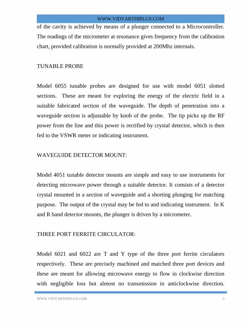
BLOCK DIAGRAM
MODEL GRAPH
Gunn
Power
Supply
Gunn
Oscillator
With mount
PIN
Modulator
Isolator
Variable
Attenuator
Frequency
Meter
Detector
Mount
CRO /
VSWR
meter
WWW.VIDYARTHIPLUS.COM
WWW.VIDYARTHIPLUS.COM 8
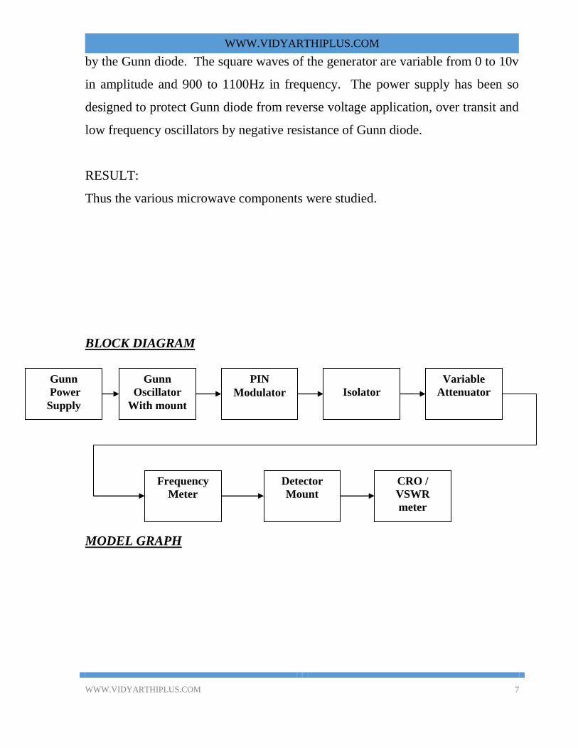
G U N N BIAS [VOLTS]
CHARACTERISTICS OF GUNN DIODE OSCILLATOR
Aim : To plot the characteristics of Gunn diode oscillator.
Apparatus/Components Required :
1. Gunn Power supply 2. Gunn oscillator with mount 3. PIN modulator
4. Isolator 5. Variable Attenuator 6. Frequency meter
7. Detector Mount 8. CRO 9. Probes
10. Cooling Fan 11. Stands
Theory :
Gunn diodes are made up of bulk semiconductor materials like Gallium
Arsenide[GaAs],Indium Phosphide[InP] and Cadmium Telluride[CdTe] which
G U N N BIAS [VOLTS] G U N N BIAS [VOLTS]
WWW.VIDYARTHIPLUS.COM
WWW.VIDYARTHIPLUS.COM 9
exhibit negative resistance. Initially for a range of bias voltages the current
increases with voltage and later starts decreasing with increase in bias voltage. In
this negative resistance region they exhibit Gunn effect or transfer electron effect
and generates microwave oscillatios. Gunn diode operates in 4 different modes
viz. Gunn or TT mode,LSA mode, quenched domain mode and delayed mode.
Microwave oscillations are generated in Gunn or TT mode. A Gunn diode
oscillator is designed by mounting the diode inside a waveguide cavity formed by
a short circuit termination at one end and by an Iris at the other end.
Precautions :
1. Before switching ON the Gunn power supply ensure that the Gunn Bias
voltage knob is in the minimum position[Left extreme] and the PIN Bias
voltage knob is in the middle position.
2. While doing the experiment ensure that the Gunn Bias voltage does not
exceed 9 Volts.
3. Before switching OFF the Gunn Bias power supply ensure that the Gunn Bias
voltage knob is in the minimum position[Left extreme].
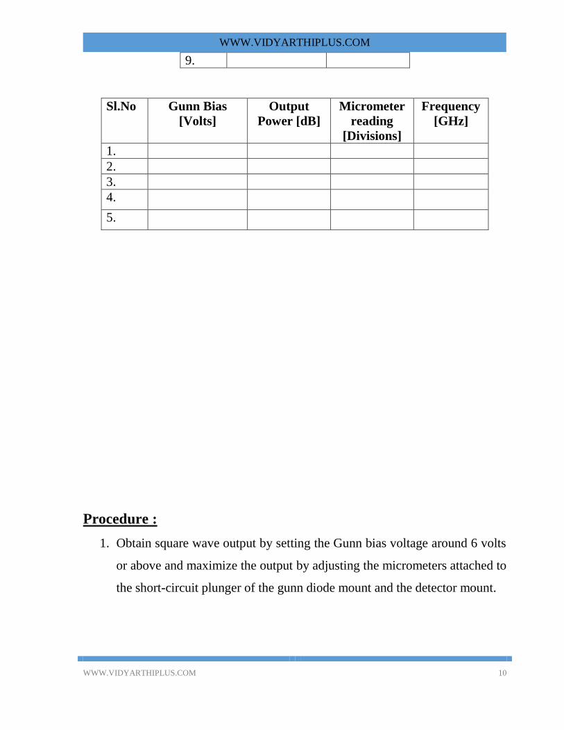
1. V-I Characteristics :
Sl.No Gunn Bias
[Volts]
Current
[mA]
1.
2.
3.
4.
5.
6.
7.
8.
WWW.VIDYARTHIPLUS.COM
WWW.VIDYARTHIPLUS.COM 10
9.
Sl.No Gunn Bias
[Volts]
Output
Power [dB]
Micrometer
reading
[Divisions]
Frequency
[GHz]
1.
2.
3.
4.
5.
Procedure :
1. Obtain square wave output by setting the Gunn bias voltage around 6 volts
or above and maximize the output by adjusting the micrometers attached to
the short-circuit plunger of the gunn diode mount and the detector mount.
WWW.VIDYARTHIPLUS.COM
WWW.VIDYARTHIPLUS.COM 11
2. Now starting from 0 Volt vary the Gunn bias in steps of 1 Volt up to a
maximum of 9 Volts. Note down the corresponding currents from the
milliammeter.
3. Tabulate the readings and plot the V-I characteristics.
4. In the region of oscillations i.e. for Gunn bias voltages in the range 6-9
Volts, for different bias voltages tune the frequency meter and observe dip
in the output and the corresponding micrometer position. After noting
down the micrometer reading, release[detune] the frequency meter and
connect the detector output to VSWR/POWER meter and note down the
output power.
5. Tabulate the readings and plot the input-output characteristics[output
power Vs Gunn bias voltage] and the frequency response[Frequency Vs
Gunn bias vltage].
Result :
Thus the characteristics of Gunn diode has been plotted.
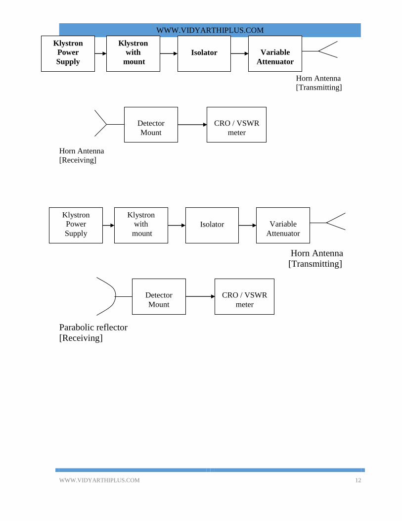
BLOCK DIAGRAM
WWW.VIDYARTHIPLUS.COM
WWW.VIDYARTHIPLUS.COM 12
Horn Antenna
[Transmitting]
Horn Antenna
[Receiving]
Horn Antenna
[Transmitting]
Parabolic reflector
[Receiving]
Klystron
Power
Supply
Klystron
with
mount
Isolator
Variable
Attenuator
Detector
Mount
CRO / VSWR
meter
Klystron
Power
Supply
Klystron
with
mount
Isolator
Variable
Attenuator
Detector
Mount
CRO / VSWR
meter
WWW.VIDYARTHIPLUS.COM
WWW.VIDYARTHIPLUS.COM 13
RADIATION PATTERN OF HORN/PARABOLIC
REFLECTOR ANTENNA
Aim : To plot the radiation pattern of horn and parabolic reflector antenna.
Apparatus/Components Required :
1. Klystron Power supply 2. Klystron with mount
3. Isolator 4. Variable Attenuator
5. Horn Antenna[2 nos] 6. Detector Mount
7. CRO 8. Probes
9. Cooling Fan 10. Stands
11. Parabolic reflector antenna
Theory :
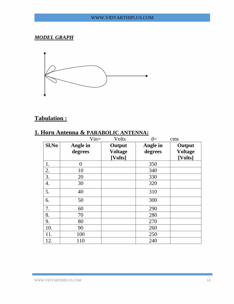
Radiation pattern of an antenna is obtained by plotting the voltage or
power or gain at various angles from the antenna. Both horn and parabolic
reflector antenna the radiation pattern is uni-directional i.e. maximum energy is
radiated in a particular direction and in other directions minimum or zero
radiation. In addition to the major lobe there may be few minor side lobes
existing. Half-power or 3-dB beam width may be found by measuring the angle
between the two half-power points or the 3-dB points or the angle between two
points where the voltage is Vmax/√2. Similarly the beam width between first
nulls[BWFN] may be found by measuring the angle between two tangential lines
to the major lobe from the origin.
WWW.VIDYARTHIPLUS.COM
WWW.VIDYARTHIPLUS.COM 14
MODEL GRAPH
Tabulation :
1. Horn Antenna & PARABOLIC ANTENNA: Vin= Volts d= cms
Sl.No Angle in
degrees
Output
Voltage
[Volts]
Angle in
degrees
Output
Voltage
[Volts]
1. 0 350
2. 10 340
3. 20 330
4. 30 320
5. 40 310
6. 50 300
7. 60 290
8. 70 280
9. 80 270
10. 90 260
11. 100 250
12. 110 240
WWW.VIDYARTHIPLUS.COM
WWW.VIDYARTHIPLUS.COM 15
Precautions :
1. Before switching ON the Klystron power supply ensure that the beam
voltage knob is in the minimum position[Left extreme] and the repeller
voltage knob is in the maximum position[right extreme].
2. While doing the experiment ensure that the beam voltage and beam current
do not exceed 250 Volts and 20 mA respectively.
3. Before switching OFF the Klystron power supply ensure that the beam
voltage knob is in the minimum position [Left extreme] and the repeller
voltage knob is in the maximum position [right extreme].
Procedure :
1. Obtain square wave output without the antenna in the set-up and maximize
the output by adjusting beam voltage, repeller voltage, modulating
amplitude and the attenuator and note down this voltage as Vin.
2. Now connect the two horn antenna in the set-up and align the two antenna
both vertically and horizontally for maximum output. Ensure a minimum
distance(end to end) of 15 cms between the antenna.
3. Set the angle where maximum output obtained as zero degrees and note
down the output voltage.
4. Vary the angle from zero degrees through 360 degrees and note down the
corresponding output voltages. Tabulate the readings.
5. Plot the Output voltage Vs Angle in degrees in a polar sheet.
6. Find the 3dB beam width and BWFN.
7. Repeat steps 1 to 6 with parabolic reflector antenna in the receiving
antenna position instead of horn antenna.
Result :
Thus the radiation pattern of horn and parabolic reflector antenna were
plotted and the 3-dB beamwidth and BWFN were found to be :
3-dB beamwidth = degrees
BWFN = degrees
WWW.VIDYARTHIPLUS.COM
WWW.VIDYARTHIPLUS.COM 16
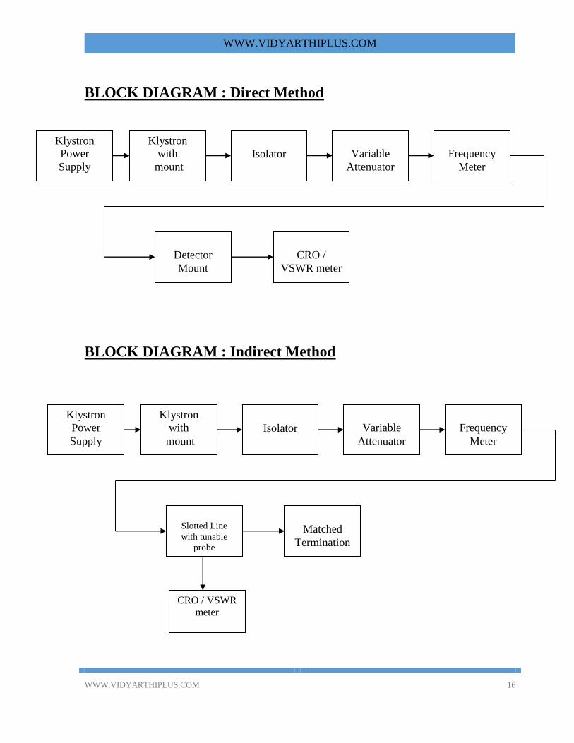
BLOCK DIAGRAM : Direct Method
BLOCK DIAGRAM : Indirect Method
Klystron
Power
Supply
Klystron
with
mount
Isolator
Variable
Attenuator
Frequency
Meter
Detector
Mount
CRO /
VSWR meter
CRO / VSWR
meter
Klystron
Power
Supply
Klystron
with
mount
Isolator
Variable
Attenuator
Frequency
Meter
Slotted Line
with tunable
probe
Matched
Termination
WWW.VIDYARTHIPLUS.COM
WWW.VIDYARTHIPLUS.COM 17
MEASUREMENT OF WAVELENGTH AND FREQUENCY
Aim : To measure wavelength and the frequency of the microwave
signal by both direct and indirect methods.
Apparatus/Components Required : 1. Klystron Power supply 2. Klystron with mount
3. Isolator 4. Variable Attenuator
5. Frequency meter 6. Detector Mount
7. slotted line with tunable probe 8. Matched Termination
9. CRO 10. Cooling Fan
11. Probes 12. Stands
Theory :
I. DIRECT METHOD:
Frequency meter is made up of a cylindrical cavity[absorption type]. By
varying the effective height(d) of the cavity its resonance frequency (fr) may be
varied. At resonance i.e. when the incoming signal frequency matched with the
‘fr’ of the cavity, maximum energy is stored in the cavity resulting in a minimum
transmitted output.
II. INDIRECT METHOD:
While studying the standing wave pattern, the distance between two
successive minima or maxima corresponds to ‘λg/2’ or λg= 2*(distance between
WWW.VIDYARTHIPLUS.COM
WWW.VIDYARTHIPLUS.COM 18
successive minima or maxima ). The cutoff wavelength of rectangular wave
guide for dominant[TE10] mode is given by λc=2*a.
Then the free space wavelength ‘λo’ can be found using the formula:
λo= λg λc/√( λg2 + λc2) and the frequency of the signal is given by :
f = C/ λo where C = 3 X 10⁸ m/sec [Velocity of EM waves in free space].
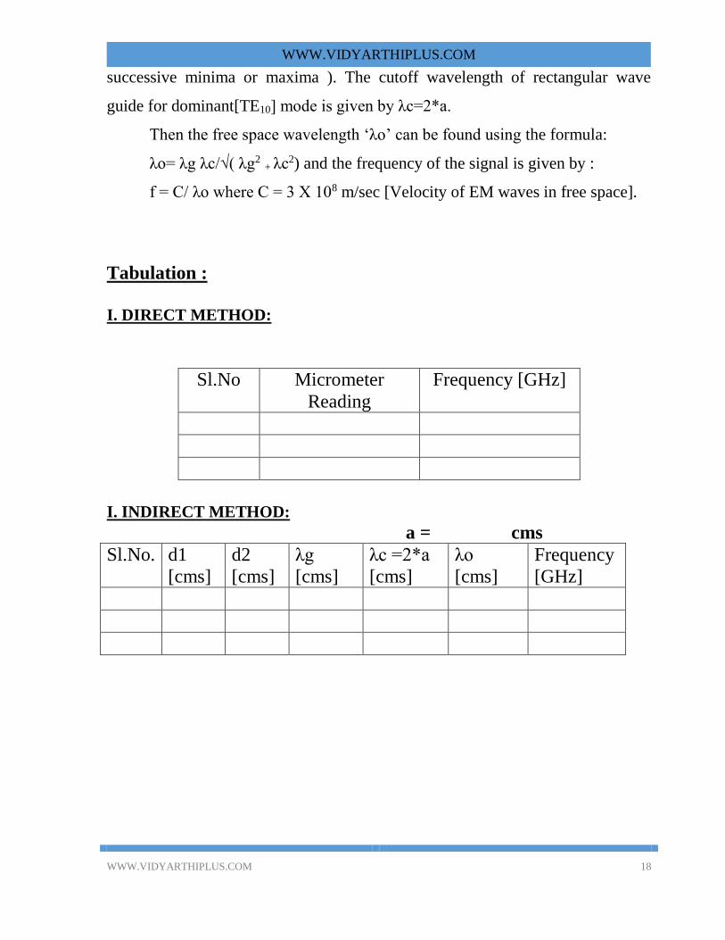
Tabulation :
I. DIRECT METHOD:
Sl.No Micrometer
Reading
Frequency [GHz]
I. INDIRECT METHOD:
a = cms
Sl.No. d1
[cms]
d2
[cms]
λg
[cms]
λc =2*a
[cms]
λo
[cms]
Frequency
[GHz]

WWW.VIDYARTHIPLUS.COM
WWW.VIDYARTHIPLUS.COM 19
Precautions :
1. Before switching ON the Klystron power supply ensure that the beam
voltage knob is in the minimum position[Left extreme] and the repeller
voltage knob is in the maximum position[right extreme].
2. While doing the experiment ensure that the beam voltage and beam current
do not exceed 250 Volts and 20 mA respectively.
3. Before switching OFF the Klystron power supply ensure that the beam
voltage knob is in the minimum position[Left extreme] and the repeller
voltage knob is in the maximum position[right extreme].
Procedure :
I.DIRECT METHOD :
1. Obtain square wave output and maximize the output by adjusting beam
voltage, repeller voltage, modulating amplitude and the attenuator.
WWW.VIDYARTHIPLUS.COM
WWW.VIDYARTHIPLUS.COM 20
2. Adjust the micrometer attached to the frequency meter till the output
becomes minimum or a dip is observed in the CRO. Now, note down the
micrometer reading.
3. Refer to the conversion chart and note down the corresponding frequency
in GHz.
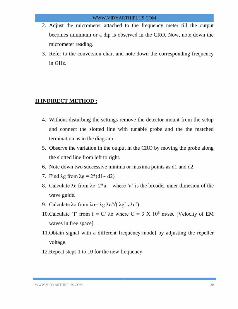
II.INDIRECT METHOD :
4. Without disturbing the settings remove the detector mount from the setup
and connect the slotted line with tunable probe and the the matched
termination as in the diagram.
5. Observe the variation in the output in the CRO by moving the probe along
the slotted line from left to right.
6. Note down two successive minima or maxima points as d1 and d2.
7. Find λg from λg = 2*(d1~ d2)
8. Calculate λc from λc=2*a where ‘a’ is the broader inner dimesion of the
wave guide.
9. Calculate λo from λo= λg λc/√( λg2 + λc2)
10. Calculate ‘f’ from f = C/ λo where C = 3 X 10⁸ m/sec [Velocity of EM
waves in free space].
11. Obtain signal with a different frequency[mode] by adjusting the repeller
voltage.
12. Repeat steps 1 to 10 for the new frequency.
WWW.VIDYARTHIPLUS.COM
WWW.VIDYARTHIPLUS.COM 21
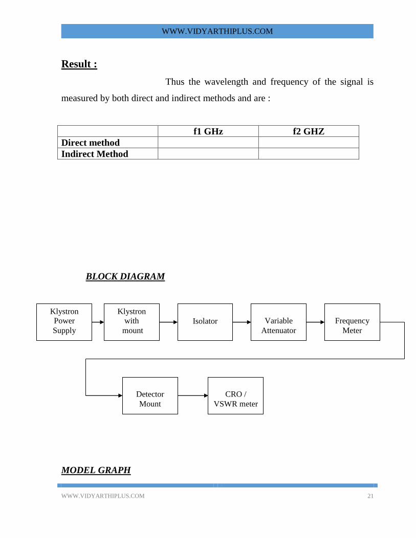
Result :
Thus the wavelength and frequency of the signal is
measured by both direct and indirect methods and are :
f1 GHz f2 GHZ
Direct method
Indirect Method
BLOCK DIAGRAM
MODEL GRAPH
Klystron
Power
Supply
Klystron
with
mount
Isolator
Variable
Attenuator
Frequency
Meter
Detector
Mount
CRO /
VSWR meter
WWW.VIDYARTHIPLUS.COM
WWW.VIDYARTHIPLUS.COM 22
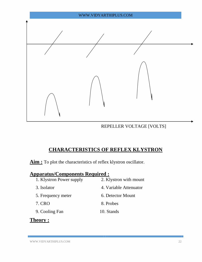
REPELLER VOLTAGE [VOLTS]
CHARACTERISTICS OF REFLEX KLYSTRON
Aim : To plot the characteristics of reflex klystron oscillator.
Apparatus/Components Required : 1. Klystron Power supply 2. Klystron with mount
3. Isolator 4. Variable Attenuator
5. Frequency meter 6. Detector Mount
7. CRO 8. Probes
9. Cooling Fan 10. Stands
Theory :
WWW.VIDYARTHIPLUS.COM
WWW.VIDYARTHIPLUS.COM 23
Reflex Klystron Oscillator works on the principle of Velocity Modulation.
The velocity of the electrons[electron beam] vary in accordance with the
variation of the RF field setup in the cavity. By varying the repeller voltage the
frequency of the signal and also the output power/voltage varies. While varying
repeller voltage continuously the output waveform[square wave] appears and
disappears several times. Each appearance of the output within a given range of
repeller voltage is called a “mode”. The method of varying the output frequency
by varying the repeller voltage is called “ Electronic tuning of reflex klystron”.
Precautions :
1. Before switching ON the Klystron power supply ensure that the beam
voltage knob is in the minimum position[Left extreme] and the repeller
voltage knob is in the maximum position[right extreme].
2.While doing the experiment ensure that the beam voltage and beam current
do not exceed 250 Volts and 20 mA respectively.
3.Before switching OFF the Klystron power supply ensure that the beam
voltage knob is in the minimum position[Left extreme] and the repeller
voltage knob is in the maximum position[right extreme].
Procedure :
1.Obtain square wave output and maximize the output by adjusting beam
voltage, repeller voltage, modulating amplitude and the attenuator.
2. For each mode note down the maximum output voltage and the
corresponding repeller voltage[X Volts] and the micrometer position for
which the output becomes minimum/disappears. Also note down the above
values for repeller voltages: X+5V and X-5V.
3.Repeat step 2 for atleast 3 different modes.

WWW.VIDYARTHIPLUS.COM
WWW.VIDYARTHIPLUS.COM 24
4.Tabulate the readings.
5.Plot the Output Vs repeller voltage and Frequency Vs repeller voltage.
Result :
Thus the characteristics of reflex klystron has been plotted .
Tabulation :
Sl.No Repeller
Voltage [Volts]
Output
Voltage
Micrometer
reading
Frequency
[GHz]

WWW.VIDYARTHIPLUS.COM
WWW.VIDYARTHIPLUS.COM 25
[Volts] [Divisions]
1.
2.
3.
4.
5.
6.
7.
8.
9.
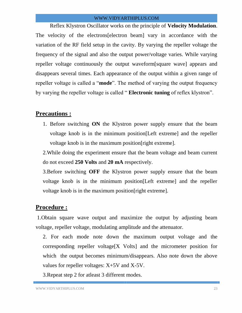
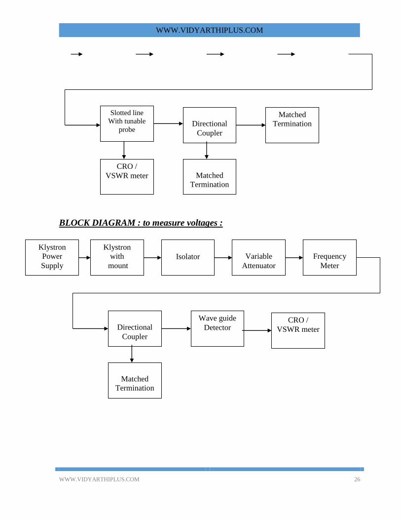
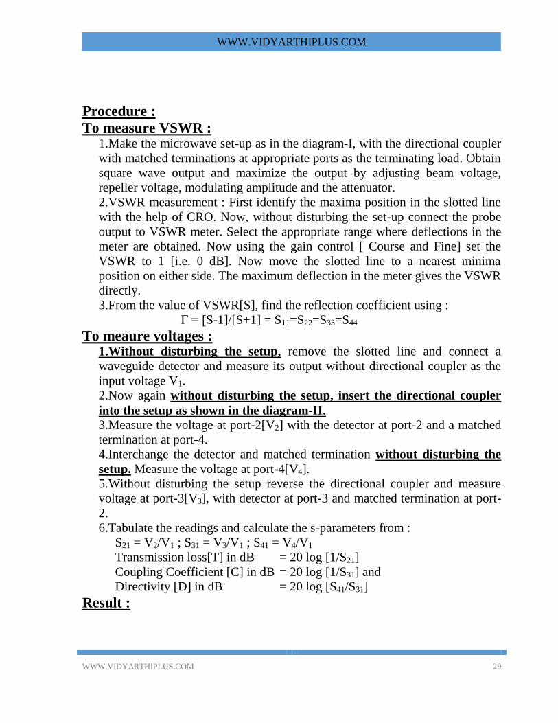
BLOCK DIAGRAM : to measure VSWR :
Klystron
Power
Supply
Klystron
with
mount
Isolator
Variable
Attenuator
Frequency
Meter
WWW.VIDYARTHIPLUS.COM
WWW.VIDYARTHIPLUS.COM 26
BLOCK DIAGRAM : to measure voltages :
Directional
Coupler
Matched
Termination
Matched
Termination
Klystron
Power
Supply
Klystron
with
mount
Isolator
Variable
Attenuator
Frequency
Meter
Directional
Coupler
Wave guide
Detector
Matched
Termination
Slotted line
With tunable
probe
CRO /
VSWR meter
CRO /
VSWR meter
WWW.VIDYARTHIPLUS.COM
WWW.VIDYARTHIPLUS.COM 27
STUDY OF DIRECTIONAL COUPLER
Aim : To study the characteristics of directional coupler and find its S-matrix.
Apparatus/Components Required : 1. Klystron Power supply 2. Klystron with mount
3. Isolator 4. Variable Attenuator
5. Frequency meter 6. Slotted line with tunable probe
7. Matched Termination__ Nos 8. Directional Coupler
9. VSWR meter 10. CRO
11. Stands 12. Probes
13. Cooling Fan
Theory :
Directional Coupler is used to couple a fraction of the input power in either
the forward or backward directions. It works on the principle of aperture
coupling. In a forward coupler desirable amount of power is coupled in the
forward direction through single, two or multiple holes[apertures]. In the
backward direction the amount of power coupled is ideally zero, but practically
there may be a meager[negligible] amount of power which is absorbed by the
matched termination connected internally. Hence practically it remains a closed
port. Ideal values for the parameters are as below :
Main line VSWR = 1
Transmission loss = 10 log[P1/P2] = 20 log[V1/V2] = 0 dB
Coupling coefficient = 10 log[P1/P4]=20 log[V1/V4] is a design parameter
Directivity = 10 log[P4/P3] = 20 log[V4/V3] = ∞ dB
Precautions : 1.Before switching on the Klystron power supply ensure that the beam voltage
knob is in the minimum position[Left extreme] and the repeller voltage knob
is in the maximum position[right extreme].
2.While doing the experiment ensure that the beam voltage and beam current
do not exceed 250 Volts and 20 mA respectively.
3.Before switching off the Klystron power supply ensure that the beam
voltage knob is in the minimum position[Left extreme] and the repeller
voltage knob is in the maximum position[right extreme].
3 4
4 1 2
WWW.VIDYARTHIPLUS.COM
WWW.VIDYARTHIPLUS.COM 28
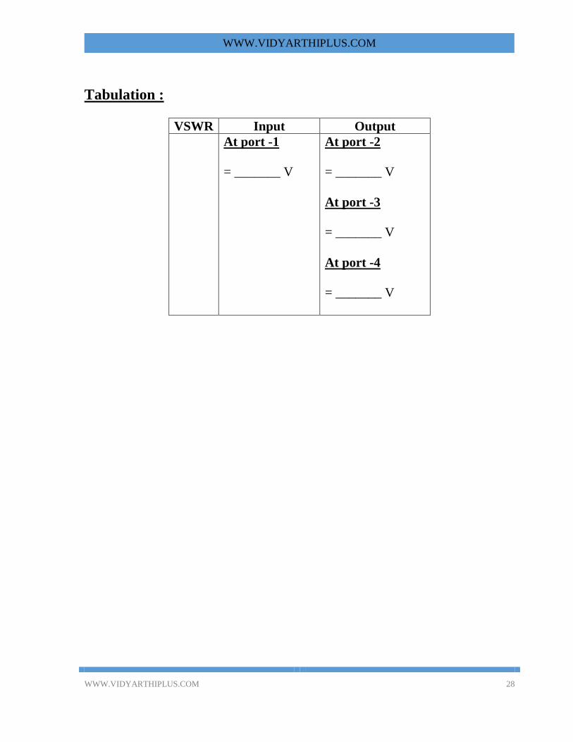
Tabulation :
VSWR Input Output
At port -1
= _______ V
At port -2
= _______ V
At port -3
= _______ V
At port -4
= _______ V
WWW.VIDYARTHIPLUS.COM
WWW.VIDYARTHIPLUS.COM 29
Procedure :
To measure VSWR : 1.Make the microwave set-up as in the diagram-I, with the directional coupler
with matched terminations at appropriate ports as the terminating load. Obtain
square wave output and maximize the output by adjusting beam voltage,
repeller voltage, modulating amplitude and the attenuator.
2.VSWR measurement : First identify the maxima position in the slotted line
with the help of CRO. Now, without disturbing the set-up connect the probe
output to VSWR meter. Select the appropriate range where deflections in the
meter are obtained. Now using the gain control [ Course and Fine] set the
VSWR to 1 [i.e. 0 dB]. Now move the slotted line to a nearest minima
position on either side. The maximum deflection in the meter gives the VSWR
directly.
3.From the value of VSWR[S], find the reflection coefficient using :
Γ = [S-1]/[S+1] = S11=S22=S33=S44
To meaure voltages :
1.Without disturbing the setup, remove the slotted line and connect a
waveguide detector and measure its output without directional coupler as the
input voltage V1.
2.Now again without disturbing the setup, insert the directional coupler
into the setup as shown in the diagram-II. 3.Measure the voltage at port-2[V2] with the detector at port-2 and a matched
termination at port-4.
4.Interchange the detector and matched termination without disturbing the
setup. Measure the voltage at port-4[V4].
5.Without disturbing the setup reverse the directional coupler and measure
voltage at port-3[V3], with detector at port-3 and matched termination at port-
2.
6.Tabulate the readings and calculate the s-parameters from :
S21 = V2/V1 ; S31 = V3/V1 ; S41 = V4/V1
Transmission loss[T] in dB = 20 log [1/S21]
Coupling Coefficient [C] in dB = 20 log [1/S31] and
Directivity [D] in dB = 20 log [S41/S31]
Result :
WWW.VIDYARTHIPLUS.COM
WWW.VIDYARTHIPLUS.COM 30
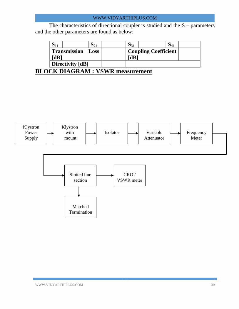
The characteristics of directional coupler is studied and the S – parameters
and the other parameters are found as below:
S11 S21 S31 S41
Transmission Loss
[dB]
Coupling Coefficient
[dB]
Directivity [dB]
BLOCK DIAGRAM : VSWR measurement
Klystron
Power
Supply
Klystron
with
mount
Isolator
r
Variable
Attenuator
Frequency
Meter
Slotted line
section
CRO /
VSWR meter
Matched
Termination
WWW.VIDYARTHIPLUS.COM
WWW.VIDYARTHIPLUS.COM 31
VSWR MEASUREMENT
AIM:
To measure VSWR introduced by the wave guide in dominant mode
of propagation.
COMPONENTS REQUIRED:
1. Microwave source (klystron power supply)
2. Klystron Mount
3. Isolator
4. Variable Attenuator
5. Slotted section
6. Matched Termination
7. VSWR meter (or) CRO
FORMULA: VSWR = V max / V min
Precautions : 1.Before switching on the Klystron power supply ensure that the beam voltage
knob is in the minimum position[Left extreme] and the repeller voltage knob
is in the maximum position[right extreme].
2.While doing the experiment ensure that the beam voltage and beam current
do not exceed 250 Volts and 20 mA respectively.

WWW.VIDYARTHIPLUS.COM
WWW.VIDYARTHIPLUS.COM 32
3.Before switching off the Klystron power supply ensure that the beam
voltage knob is in the minimum position[Left extreme] and the repeller
voltage knob is in the maximum position[right extreme].
PROCEDURE:
1. Arrange the bench setup as shown in figure.
2. Adjust the probe carriage to measure V max and note the readings.
3. Adjust the probe carriage to measure V min and note the readings.
4. Use the formula to find VSWR.

WWW.VIDYARTHIPLUS.COM
WWW.VIDYARTHIPLUS.COM 33
RESULT:
Thus the VSWR introduced by the wave guide in dominant mode of
propagation was determined and verified.
WWW.VIDYARTHIPLUS.COM
WWW.VIDYARTHIPLUS.COM 34
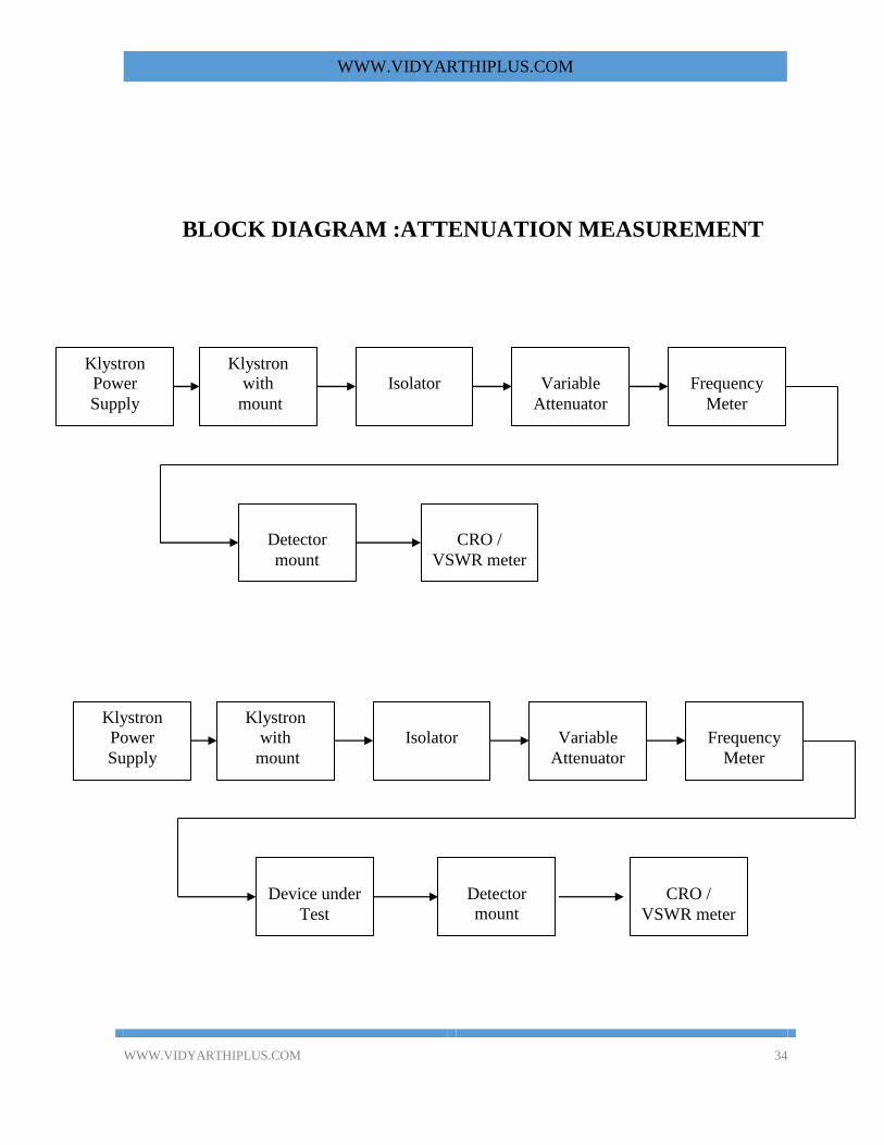
BLOCK DIAGRAM :ATTENUATION MEASUREMENT
Klystron
Power
Supply
Klystron
with
mount
Isolator
r
Variable
Attenuator
Frequency
Meter
Detector
mount
CRO /
VSWR meter
Klystron
Power
Supply
Klystron
with
mount
Isolator
r
Variable
Attenuator
Frequency
Meter
Device under
Test
Detector
mount
CRO /
VSWR meter
WWW.VIDYARTHIPLUS.COM
WWW.VIDYARTHIPLUS.COM 35
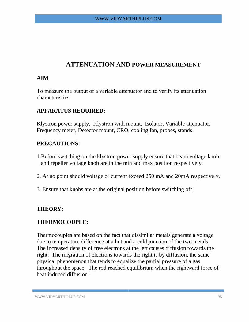
ATTENUATION AND POWER MEASUREMENT
AIM
To measure the output of a variable attenuator and to verify its attenuation
characteristics.
APPARATUS REQUIRED:
Klystron power supply, Klystron with mount, Isolator, Variable attenuator,
Frequency meter, Detector mount, CRO, cooling fan, probes, stands
PRECAUTIONS:
1.Before switching on the klystron power supply ensure that beam voltage knob
and repeller voltage knob are in the min and max position respectively.
2. At no point should voltage or current exceed 250 mA and 20mA respectively.
3. Ensure that knobs are at the original position before switching off.
THEORY:
THERMOCOUPLE:
Thermocouples are based on the fact that dissimilar metals generate a voltage
due to temperature difference at a hot and a cold junction of the two metals.
The increased density of free electrons at the left causes diffusion towards the
right. The migration of electrons towards the right is by diffusion, the same
physical phenomenon that tends to equalize the partial pressure of a gas
throughout the space. The rod reached equilibrium when the rightward force of
heat induced diffusion.

WWW.VIDYARTHIPLUS.COM
WWW.VIDYARTHIPLUS.COM 36
MODERN POWER METER:
A 16- bit analog digital converter (ADC) processes the average power signal.
A highly sophisticated video amplifier design is implemented for the normal
path to pressure envelop fidelity and accuracy. The central gun for peak and
average power meters is to provide reliable accurate and fast characteristics of
pulsed and complex modulation envelops. The meters excel in versatility
featuring a techniques called time gated measurements.
PROCEDURE:
1. Set the micro bench as per the block diagram.
2. Initial setting in the power meter is set.
3. Resolution→ 0.1 db]
4. Select absolute unit option and select dbm.
5. Select bar graph required.
6. Select the band as X
7. Select the number of samples/sec as 100/sec.
8. Enter the switch, which is used to store the selected mean option.
9. Escape switch is used to cancel any command.
10. The maximum output power is obtained by properly adjusting the klystron
power supply.
11. By varying the variable attenuator corresponding output power is
measured from the power meter.
12. A graph is drawn between micrometer reading of VA and power meter.
RESULT:
WWW.VIDYARTHIPLUS.COM
WWW.VIDYARTHIPLUS.COM 37
Thus the output of a variable attenuator was measured and its characteristics
were verified.
CIRCUIT DIAGRAM:
Model Graph :
P-I Characteristics V-I Characteristics
P
0
w
Optical
Power
Meter
OFC
Vbias
(1-10V)
180
ohms R2
VLED

WWW.VIDYARTHIPLUS.COM
WWW.VIDYARTHIPLUS.COM 38
e
r
(μ
W) C U R R E N T [mA] V O L T AG E [Volts]
WWW.VIDYARTHIPLUS.COM
WWW.VIDYARTHIPLUS.COM 39
DC CHARACTERISTICS OF LED
Aim : To plot the VI and PI characteristics of LED operating at 850 nm
wavelength and find the conversion efficiency.
Apparatus Required :
1. OFT powers supply
2. LED module
3. Optical power meter
4. Bare Fiber adapter-Plastic
5. 1.25m plastic fiber
6. 180 Ω resistor
7. Digital multimeter
Theory :
LEDs, used in optical communication have high modulation rate
capability, high radiance, high reliability and emission wavelengths restricted to
the near-IR spectral regions of low attenuation in fibers. The materials used are
GaAs, InGaAs. The internal quantum efficiency is only 1% and external
efficiency is much lower due to light emitted from semiconductor-air surface,
angle of incidence, the light reflected back and absorption at the point of
generation and emitting surface. Recombination of excess electrons and holes
takes place whenever current is passed through the PN junction of LED. The
energy released by photons results in light emission.
Precautions :
1. Before switching on the power supply ensure that the
potentiometer[R2] is in the minimum position[Left extreme].
2. After completing the experiment before switching of the power
supply to the LD module ensure that the potentiometer[R2] is in the
minimum position[Left extreme].

WWW.VIDYARTHIPLUS.COM
WWW.VIDYARTHIPLUS.COM 40
Tabulation :
Vf volts If mA VLED volts Power
[dBm]
Power in
μW [Po]

WWW.VIDYARTHIPLUS.COM
WWW.VIDYARTHIPLUS.COM 41
Procedure :
1. Make the set-up as in the diagram.
2. With potentiometer in the minimum position switch on the power
supply.
3. Measure the voltage across resistor R1 and note down as V1;
4. Measure the voltage across the LED and note it as VLED; Also note
down the corresponding output power in dBm from the optical power
meter.
5. Calculate If from the formula: If = V1/180.
6. Calculate power in microwatts from the formula :
Power[μW] = 1mW * 10 [Power in dBm/10]
7. Vary the potentiometer slowly and for various values of V1 repeat
steps 3 to 6.
8. Tabulate the readings.
9. Plot the VI characteristics taking VLED in the x-axis and If in the y-
axis.
10. Plot the P-I characteristics taking If in the x-axis and the Power in
watts in the y-axis.
11. By taking the average values of power in watts, VLED and If and using
the following formula calculate the conversion efficiency:
η = [Po*100/ (VLED* If)] %
WWW.VIDYARTHIPLUS.COM
WWW.VIDYARTHIPLUS.COM 42
Result :
Thus the VI and PI characteristics of LED was plotted and the conversion
efficiency is found as ___________________.
CIRCUIT DIAGRAM:
Model Graph :
P-I Characteristics V-I Characteristics
P
0
L
D
U
N
I
T
Opt
ical
Po
wer
Met
er
R1 R2
VLD
VPD
Vbias
WWW.VIDYARTHIPLUS.COM
WWW.VIDYARTHIPLUS.COM 43
w
e
r
(μ
W) C U R R E N T [mA] V O L T AG E [Volts]
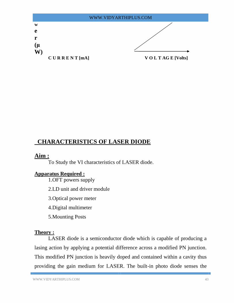
CHARACTERISTICS OF LASER DIODE
Aim : To Study the VI characteristics of LASER diode.
Apparatus Required :
1.OFT powers supply
2.LD unit and driver module
3.Optical power meter
4.Digital multimeter
5.Mounting Posts
Theory :
LASER diode is a semiconductor diode which is capable of producing a
lasing action by applying a potential difference across a modified PN junction.
This modified PN junction is heavily doped and contained within a cavity thus
providing the gain medium for LASER. The built-in photo diode senses the
WWW.VIDYARTHIPLUS.COM
WWW.VIDYARTHIPLUS.COM 44
light sent from the LD and the output of this PD can be used as feedback for
controlling the current through the LD. Light from LD is directional.
Precautions :
1.Before switching on the power supply ensure that the potentiometer[R2]
is in the minimum position[Left extreme].
2.After completing the experiment before switching of the power supply
to the LD module ensure that the potentiometer[R2] is in the minimum
position[Left extreme].
Tabulation :
V1 volts ILD mA VLD volts Power
[dBm]
Power in
μW

WWW.VIDYARTHIPLUS.COM
WWW.VIDYARTHIPLUS.COM 45
WWW.VIDYARTHIPLUS.COM
WWW.VIDYARTHIPLUS.COM 46
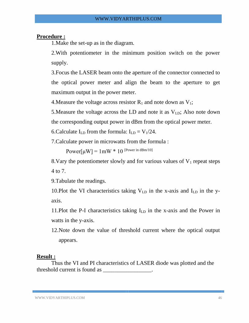
Procedure :
1.Make the set-up as in the diagram.
2.With potentiometer in the minimum position switch on the power
supply.
3.Focus the LASER beam onto the aperture of the connector connected to
the optical power meter and align the beam to the aperture to get
maximum output in the power meter.
4.Measure the voltage across resistor R1 and note down as V1;
5.Measure the voltage across the LD and note it as VLD; Also note down
the corresponding output power in dBm from the optical power meter.
6.Calculate ILD from the formula: ILD = V1/24.
7.Calculate power in microwatts from the formula :
Power[μW] = 1mW * 10 [Power in dBm/10]
8.Vary the potentiometer slowly and for various values of V1 repeat steps
4 to 7.
9.Tabulate the readings.
10.Plot the VI characteristics taking VLD in the x-axis and ILD in the y-
axis.
11.Plot the P-I characteristics taking ILD in the x-axis and the Power in
watts in the y-axis.
12. Note down the value of threshold current where the optical output
appears.
Result :
Thus the VI and PI characteristics of LASER diode was plotted and the
threshold current is found as _________________.
WWW.VIDYARTHIPLUS.COM
WWW.VIDYARTHIPLUS.COM 47
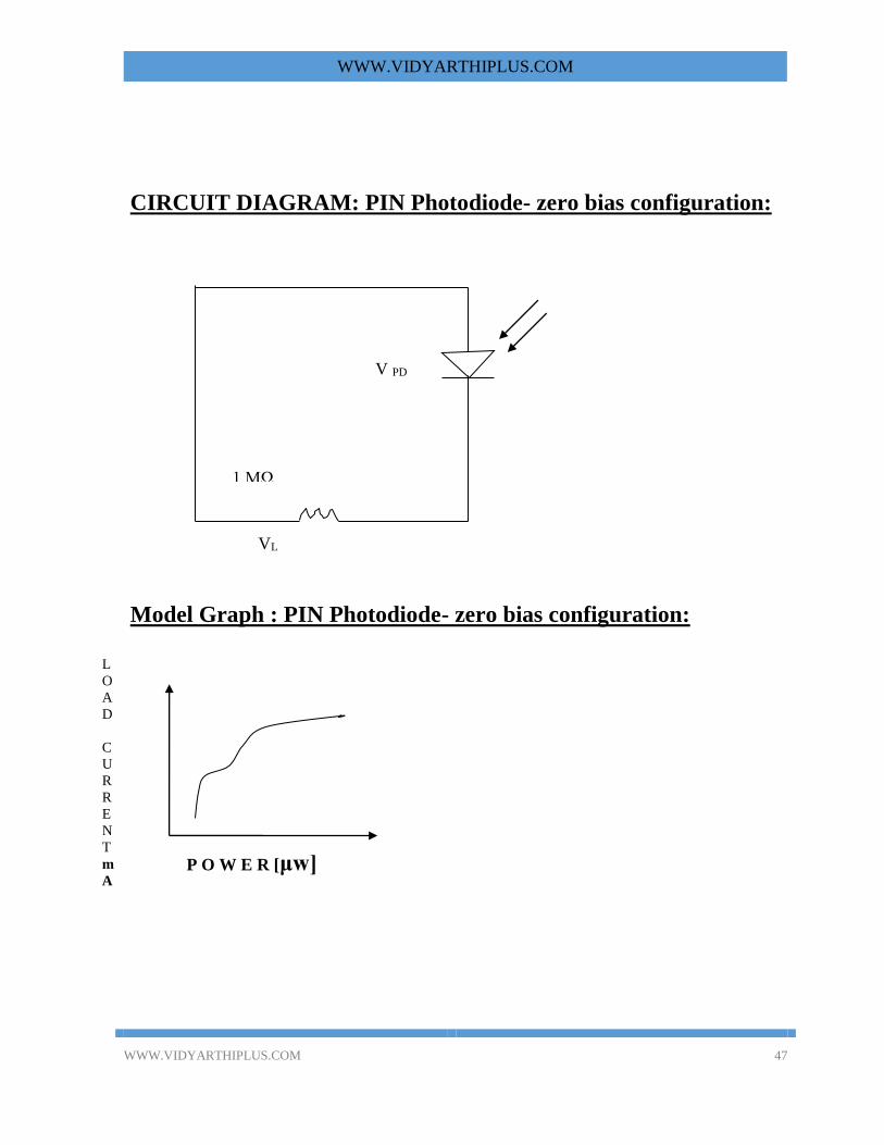
CIRCUIT DIAGRAM: PIN Photodiode- zero bias configuration:
Model Graph : PIN Photodiode- zero bias configuration:
P O W E R [μw]
V PD
1 MΩ
VL
L
O
A
D
C
U
R
R
E
N
T
m
A

WWW.VIDYARTHIPLUS.COM
WWW.VIDYARTHIPLUS.COM 48
WWW.VIDYARTHIPLUS.COM
WWW.VIDYARTHIPLUS.COM 49
DC CHARACTERISTICS OF PIN Photo diode
Aim : To study the zero bias, forward bias and reverse bias characteristics of
PIN photo diode and plot the VI and PI characteristics and to determine the
responsivity and quantum efficiency.
Apparatus Required :
8. OFT powers supply
9. PD module
10. Optical power meter
11. Optical power source
12. Bare Fiber adapter-Plastic
13. 1m patch cord
14. 1MΩ,10KΩ resistors
15. Digital multimeter
Theory :
If a photon having adequate energy[should be greater than the band gap]
is absorbed by a p-n junction, an electron will be transferred to the conduction
band, thereby forming a hole in the valence band. As a result, an open circuit
voltage is created and a current will flow, provided the circuit is closed through
a load resistor. In case of reverse bias p-n junction, the transit time can be made
small and it will produce current linearly proportional to the incident photon
energy. The frequency response can be improved if the p-n junction is separated
by an intrinsic region. The introduction of the intrinsic region decreases the
junction capacitance. This is called ‘Positive Intrinsic Negative’[PIN] photo
diode. For high frequency operation, the PIN diode can be made as small as
practical, to match the size of the spot of the optical beam.

WWW.VIDYARTHIPLUS.COM
WWW.VIDYARTHIPLUS.COM 50
Tabulation : PIN Photo Diode- zero bias configuration:
Power
[dBm]
VL volts PO [μW] Iz mA
CIRCUIT DIAGRAM: PIN Photo Diode- forward bias
configuration:
WWW.VIDYARTHIPLUS.COM
WWW.VIDYARTHIPLUS.COM 51
Procedure :
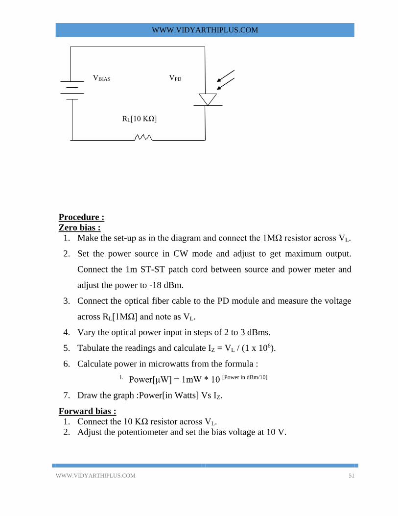
Zero bias :
1. Make the set-up as in the diagram and connect the 1MΩ resistor across VL.
2. Set the power source in CW mode and adjust to get maximum output.
Connect the 1m ST-ST patch cord between source and power meter and
adjust the power to -18 dBm.
3. Connect the optical fiber cable to the PD module and measure the voltage
across RL[1MΩ] and note as VL.
4. Vary the optical power input in steps of 2 to 3 dBms.
5. Tabulate the readings and calculate IZ = VL / (1 x 10⁶).
6. Calculate power in microwatts from the formula :
i. Power[μW] = 1mW * 10 [Power in dBm/10]
7. Draw the graph :Power[in Watts] Vs IZ.
Forward bias :
1. Connect the 10 KΩ resistor across VL.
2. Adjust the potentiometer and set the bias voltage at 10 V.
RL[10 KΩ]
VBIAS VPD
WWW.VIDYARTHIPLUS.COM
WWW.VIDYARTHIPLUS.COM 52
3. Set the power source in CW mode and adjust to get maximum output.
Connect the 1m ST-ST patch cord between source and power meter and
adjust the power to -18 dBm.
4. Connect the optical fiber cable to the PD module and measure the voltage
across RL[10 KΩ] and note as VL.
5. Vary the optical power in steps of 2 to 3 dBm and note down the
corresponding VL.
6. Calculate IF = VL / (1 x 10⁴).
7. Plot the graph : Power in Watts Vs IF.
8. Now, fix the optical power at some constant value say -10 dBm and vary
the VBIAS from 1V to 10 V in steps of 1 V and note down the
corresponding VL.
9. Plot VBIAS Vs IF.
Model Graph : PIN Photo Diode- forward bias configuration:
WWW.VIDYARTHIPLUS.COM
WWW.VIDYARTHIPLUS.COM 53
V BIAS [V]
F
O C
R U
W R
A R
R E
D N
T
[mA]
Power [μW]
F
O C
R U
W R
A R
R E
D N
T
[mA]
WWW.VIDYARTHIPLUS.COM
WWW.VIDYARTHIPLUS.COM 54
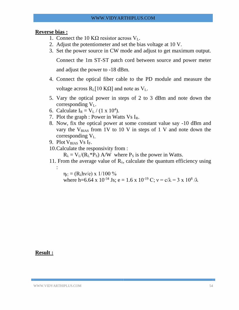
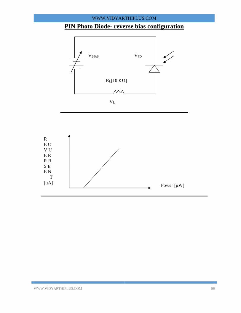
Reverse bias :
1. Connect the 10 KΩ resistor across VL.
2. Adjust the potentiometer and set the bias voltage at 10 V.
3. Set the power source in CW mode and adjust to get maximum output.
Connect the 1m ST-ST patch cord between source and power meter
and adjust the power to -18 dBm.
4. Connect the optical fiber cable to the PD module and measure the
voltage across RL[10 KΩ] and note as VL.
5. Vary the optical power in steps of 2 to 3 dBm and note down the
corresponding VL.
6. Calculate IR = VL / (1 x 10⁴).
7. Plot the graph : Power in Watts Vs IR.
8. Now, fix the optical power at some constant value say -10 dBm and
vary the VBIAS from 1V to 10 V in steps of 1 V and note down the
corresponding VL.
9. Plot VBIAS Vs IF.
10. Calculate the responsivity from :
Rλ = VL/(RL*PS) A/W where PS is the power in Watts.
11. From the average value of Rλ, calculate the quantum efficiency using
:
ηC = (Rλhν/e) x 1/100 %
where h=6.64 x 10⁻³⁴ Js; e = 1.6 x 10⁻¹⁹ C; ν = c/λ = 3 x 10⁸ /λ
Result :
WWW.VIDYARTHIPLUS.COM
WWW.VIDYARTHIPLUS.COM 55
Thus zero bias, forward bias and reverse bias characteristics of PIN Photo
diode were plotted and the responsivity and quantum efficiency were found to
be ___________________ and _____________________.
Tabulation : PIN Photo Diode- forward bias configuration:
VBIAS = ____V
P[dBm] PO[μW] VL[V] IF[mA]
P = -_____ dBm VBIAS[V] VL mV IF [mA]
WWW.VIDYARTHIPLUS.COM
WWW.VIDYARTHIPLUS.COM 56
PIN Photo Diode- reverse bias configuration
Power [μW]
R
E C
V U
E R
R R
S E
E N
T
[μA]
RL[10 KΩ]
VBIAS VPD
VL

WWW.VIDYARTHIPLUS.COM
WWW.VIDYARTHIPLUS.COM 57
Tabulation : PIN Photo Diode- reverse bias configuration:
VBIAS = ______ V
P[dBm] PO[μW] VL[V] IR[μA]
P[dBm] = ________ dBm VBIAS[V] VL mV IR [mA]
WWW.VIDYARTHIPLUS.COM
WWW.VIDYARTHIPLUS.COM 58
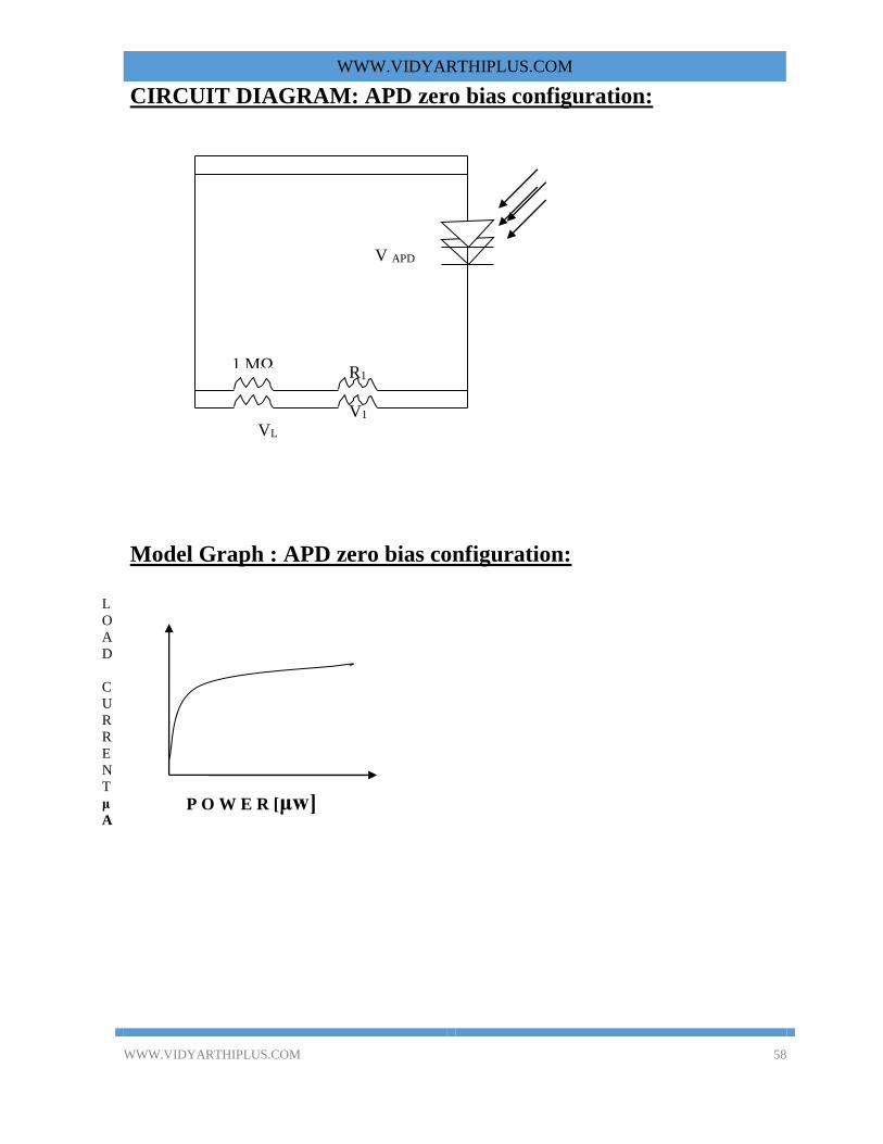
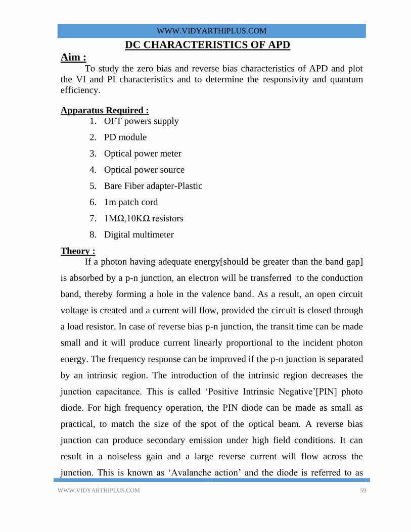
CIRCUIT DIAGRAM: APD zero bias configuration:
Model Graph : APD zero bias configuration:
P O W E R [μw]
V APD
V1
R1 1 MΩ
VL
L
O
A
D
C
U
R
R
E
N
T
μ
A
WWW.VIDYARTHIPLUS.COM
WWW.VIDYARTHIPLUS.COM 59
DC CHARACTERISTICS OF APD
Aim : To study the zero bias and reverse bias characteristics of APD and plot
the VI and PI characteristics and to determine the responsivity and quantum
efficiency.
Apparatus Required :
1. OFT powers supply
2. PD module
3. Optical power meter
4. Optical power source
5. Bare Fiber adapter-Plastic
6. 1m patch cord
7. 1MΩ,10KΩ resistors
8. Digital multimeter
Theory :
If a photon having adequate energy[should be greater than the band gap]
is absorbed by a p-n junction, an electron will be transferred to the conduction
band, thereby forming a hole in the valence band. As a result, an open circuit
voltage is created and a current will flow, provided the circuit is closed through
a load resistor. In case of reverse bias p-n junction, the transit time can be made
small and it will produce current linearly proportional to the incident photon
energy. The frequency response can be improved if the p-n junction is separated
by an intrinsic region. The introduction of the intrinsic region decreases the
junction capacitance. This is called ‘Positive Intrinsic Negative’[PIN] photo
diode. For high frequency operation, the PIN diode can be made as small as
practical, to match the size of the spot of the optical beam. A reverse bias
junction can produce secondary emission under high field conditions. It can
result in a noiseless gain and a large reverse current will flow across the
junction. This is known as ‘Avalanche action’ and the diode is referred to as

WWW.VIDYARTHIPLUS.COM
WWW.VIDYARTHIPLUS.COM 60
‘Avalanche Photo diode’[APD].It has internal gain and its responsivity is better
than that of PN or PIN photodiode. Its internal gain yields much better S/N
Tabulation : APD zero bias configuration:
Power
[dBm]
VL volts PO [μW] IL μA
CIRCUIT DIAGRAM: APD reverse bias configuration:
WWW.VIDYARTHIPLUS.COM
WWW.VIDYARTHIPLUS.COM 61
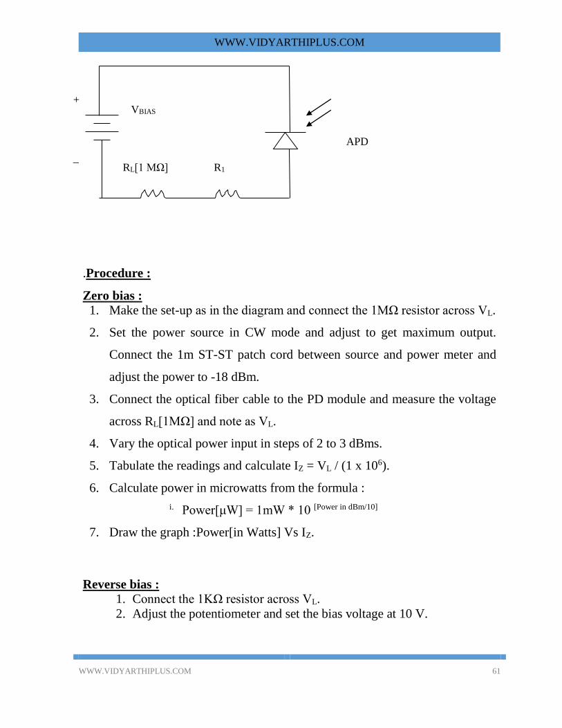
.Procedure :
Zero bias :
1. Make the set-up as in the diagram and connect the 1MΩ resistor across VL.
2. Set the power source in CW mode and adjust to get maximum output.
Connect the 1m ST-ST patch cord between source and power meter and
adjust the power to -18 dBm.
3. Connect the optical fiber cable to the PD module and measure the voltage
across RL[1MΩ] and note as VL.
4. Vary the optical power input in steps of 2 to 3 dBms.
5. Tabulate the readings and calculate IZ = VL / (1 x 10⁶).
6. Calculate power in microwatts from the formula :
i. Power[μW] = 1mW * 10 [Power in dBm/10]
7. Draw the graph :Power[in Watts] Vs IZ.
Reverse bias :
1. Connect the 1KΩ resistor across VL.
2. Adjust the potentiometer and set the bias voltage at 10 V.
RL[1 MΩ] R1
VBIAS
APD
+
_
WWW.VIDYARTHIPLUS.COM
WWW.VIDYARTHIPLUS.COM 62
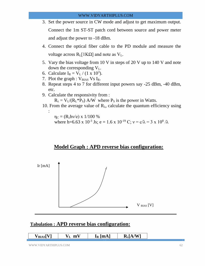
3. Set the power source in CW mode and adjust to get maximum output.
Connect the 1m ST-ST patch cord between source and power meter
and adjust the power to -18 dBm.
4. Connect the optical fiber cable to the PD module and measure the
voltage across RL[1KΩ] and note as VL.
5. Vary the bias voltage from 10 V in steps of 20 V up to 140 V and note
down the corresponding VL.
6. Calculate IR = VL / (1 x 10³).
7. Plot the graph : VBIAS Vs IR.
8. Repeat steps 4 to 7 for different input powers say -25 dBm, -40 dBm,
etc.
9. Calculate the responsivity from :
Rλ = VL/(RL*PS) A/W where PS is the power in Watts.
10. From the average value of Rλ, calculate the quantum efficiency using
:
ηC = (Rλhν/e) x 1/100 %
where h=6.63 x 10⁻³ Js; e = 1.6 x 10⁻¹⁹ C; ν = c/λ = 3 x 10⁸ /λ
Model Graph : APD reverse bias configuration:
Tabulation : APD reverse bias configuration:
VBIAS[V] VL mV IR [mA] Rλ[A/W]
V BIAS [V]
Ir [mA]

WWW.VIDYARTHIPLUS.COM
WWW.VIDYARTHIPLUS.COM 63

WWW.VIDYARTHIPLUS.COM
WWW.VIDYARTHIPLUS.COM 64
Result :
Thus zero bias and reverse bias characteristics of APD were plotted and
the quantum efficiency is found to be ___________________.
BLOCK DIAGRAM
WWW.VIDYARTHIPLUS.COM
WWW.VIDYARTHIPLUS.COM 65
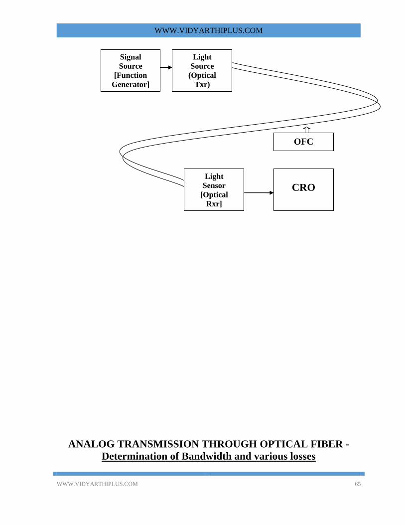
ANALOG TRANSMISSION THROUGH OPTICAL FIBER -
Determination of Bandwidth and various losses
Light
Source
(Optical
Txr)
Signal
Source
[Function
Generator]
OFC
Light
Sensor
[Optical
Rxr]
CRO
WWW.VIDYARTHIPLUS.COM
WWW.VIDYARTHIPLUS.COM 66
Aim : To establish a fiber optic analog link and determine the bandwidth,
attenuation loss, bending loss and coupling losses.
Apparatus/Components Required : 1. OFT Kit 2. CRO
3. Function Generator 4. 1m and 3m OF cables
5. 10 mm and 12 mm Mandrels 6. Jig for connecting 2 fibers
Theory :
Though optical fibers offer many advantages including very low EM
interference, the signal strength decreases as light travels longer distances. This
is because of the various losses including rayleigh scattering loss and increases
with length.
Unless proper splicing techniques are used for connecting 2 fibers there
exists considerable coupling losses due to various misalignments including
axial misalignment.
Similarly there exist two kinds of bending losses viz. micro bending loss
and constant radius bending losses. The former is because of the light absorbed
by the water/air molecules or any irregularities which could have occurred at
the time of manufacturing of the fibers. Constant radius bending losses occur
because of fiber bending during cable laying.
WWW.VIDYARTHIPLUS.COM
WWW.VIDYARTHIPLUS.COM 67
Tabulation : 1. For Bandwidth : Vin = __________ Volts
Frequency
[Hz]
Output
Voltage
[Volts]
Gain
[dB]
Tabulation : 2. For Atenuation Loss : Vin = __________ Volts
Cable Output voltage
[Volts]
1m V1=
3m V3=
Tabulation : 3. For Bending Loss :
Cable/Bend Output voltage
Voutbb[Volts]
Output voltage
Voutab[Volts]
1m / 10 mm
1m / 12 mm
3m / 10 mm
3m / 12 mm Voutbb = output voltage without any bending
Voutab = output voltage with bend
WWW.VIDYARTHIPLUS.COM
WWW.VIDYARTHIPLUS.COM 68
Procedure :
1.Make the connections as in the diagram. Connect the input signal from FG
to I/O-1. Short I/O-1,I/O-2 and P11 ________. Connect I/O-2 and the output
from P31 to the two channels of CRO. Set the switch SW8 to analog
position. Adjust the gain control knob to obtain proper shape of the output
signal.
2.[a] To measure the bandwidth of the fiber :
Note down the amplitude of input signal as Vin. Vary the frequency
of the input signal from a few Hz to MHz and note down the
corresponding output voltages. Tabulate the readings and calculate the
gain from the formula :
Gain[dB]= 20 * log[Vout/Vin].
Plot the gain Vs frequency graph. Note down the two points which
are 3 dB lower from the maximum gain on either side. Note down the
corresponding frequencies as f1 and f2; then the bandwidth of the fiber is
: [f2-f1]
[b] To measure the attenuation loss in the fiber :
Connect the 1m fiber between the Tx and Rx. Note down the input
voltage as Vin and the output voltage as V1.Replace the 1m fiber with 3m
fiber and for the same Vin note down the output as V3. Then the
attenuation loss in Np/m can be calculated from :
α[Np/m]= -[1/2]* ln[V3/V1] and α’[dB/m]= 4.343*α
WWW.VIDYARTHIPLUS.COM
WWW.VIDYARTHIPLUS.COM 69
Tabulation : 4. For coupling Loss :
Vin = __________ Volts
Coupling Output voltage
[Volts]
Without Gap
With 1 cm Gap
[c] To measure the Bending loss in the fiber :
1.Connect the 1m fiber between the Tx and Rx. Note down the
output voltage as Voutbb.Take the 10mm radius mandrel and make 1 or 2
turns of the fiber on the mandrel and note down the output as Voutab. Now
replace the 10mm mandrel with 12mm mandrel and note down the
output voltage.
2.Repeat step 1 for 3m cable.
3. Calculate the bending loss from the formula:
Bending Loss[dB]= 20*log[Voutbb/Voutab]
[d] To measure the Coupling loss in the fiber :
Connect one end of the 1m fiber to the Tx and one end of the 3m
fiber to the Rx. Connect the remaining 2 end together using the Jig
WWW.VIDYARTHIPLUS.COM
WWW.VIDYARTHIPLUS.COM 70
making the ends to touch each other. Note down the input and output
voltages.
With the same input voltage, introduce 1cm gap between the fiber
ends connected in the jig and note down the output voltage. Calculate the
coupling losses without gap and with 1cm gap using the formula:
η= 20*log [Vin / Vout] – α’[L1+L2] where α’= 4.343α and L1=
1m and L2= 3m
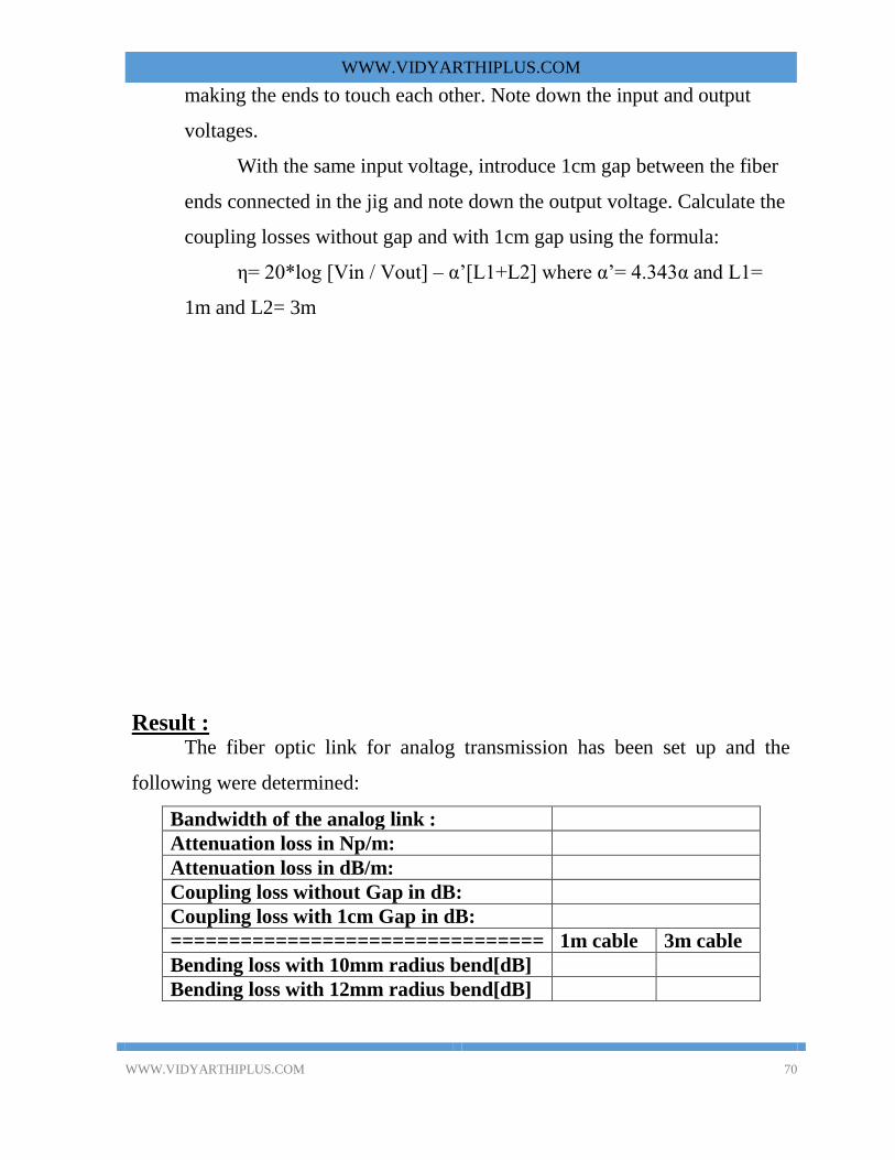
Result : The fiber optic link for analog transmission has been set up and the
following were determined:
Bandwidth of the analog link :
Attenuation loss in Np/m:
Attenuation loss in dB/m:
Coupling loss without Gap in dB:
Coupling loss with 1cm Gap in dB:
================================ 1m cable 3m cable
Bending loss with 10mm radius bend[dB]
Bending loss with 12mm radius bend[dB]
WWW.VIDYARTHIPLUS.COM
WWW.VIDYARTHIPLUS.COM 71
DETERMINATION OF NUMERICAL APERTURE
Aim : To establish a fiber optic data link and determine the numerical aperture
of the fiber and to demonstrate TDM.
Apparatus/Components Required : 1. OFT Kit 2. CRO
3. Function Generator 4. Patch cords
5. Optical fiber cable[1m,3m] 6. Jig for numerical aperture
measurement
Theory :
Large bandwidth, low attenuation are the important characteristics of
optical fibers which makes them suitable for long distance communication,
more particularly data communication. fiber systems for rates below 10 Kbps
are cheap and can be readily constructed from basic components. Data
WWW.VIDYARTHIPLUS.COM
WWW.VIDYARTHIPLUS.COM 72
rates from 100 Kbps to 10 Mbps are costly and difficult to implement.
However, with advancement in technology data rates more than 10 Mbps are
also possible.
Procedure :
To measure data rate:
Make the connections as in the diagram. Connect the data input signal
from FG to _____. Short I/O-1,I/O-2 and P11 ________. Connect I/O-2 and
the output from P31 to the two channels of CRO. Set the switch SW8 to
analog position. Adjust the gain control knob to obtain proper shape of the
output signal. Trace both input and output signals.
Tabulation : 1. For data transmission :
Input Output
Amplitude[V] Frequency[Hz] Amplitude[V] Frequency[Hz]

WWW.VIDYARTHIPLUS.COM
WWW.VIDYARTHIPLUS.COM 73
To measure the Numerical Aperture of the fiber :
1. Insert one end of the fiber into the numerical aperture measurement
2. Gently tighten the screw to hold the fiber firmly in place.
3. Connect the other end of the fiber to LED2. The fiber will project a circular
patch of the light on the screen. Let ‘d’ be the distance between the fiber tip and
the screen. Now measure the diameter of circular patch of red light in
perpendicular directions.
4.The mean radius of the circular patch is calculated from :

WWW.VIDYARTHIPLUS.COM
WWW.VIDYARTHIPLUS.COM 74
X = [DE + BC] /4
5.Calculate NA from : NA = sinθ = X /√[d2+X2]
6.Repeat the above steps fro different values of ‘d’.
7.Tabulate the readings and find the average value of NA.
Tabulation : 2. For Maximum Bit Rate :
Maximum
Bit Rate
Tabulation : 3. For Numerical Aperture :
X[cms] d[cms] NA
Average NA
Result : The fiber optic link for data transmission has been set up, TDM
demonstrated and the following were determined:
Numerical Aperture[Average] :
Data Rate :
WWW.VIDYARTHIPLUS.COM
WWW.VIDYARTHIPLUS.COM 75
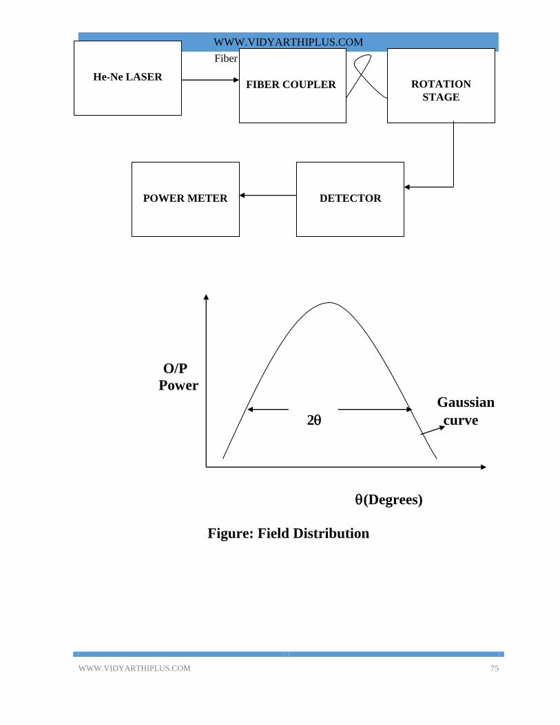
BLOCK DIAG Fiber
O/P
Power
Gaussian
2 curve
(Degrees)
Figure: Field Distribution
He-Ne LASER
FIBER COUPLER
ROTATION
STAGE
DETECTOR
POWER METER
WWW.VIDYARTHIPLUS.COM
WWW.VIDYARTHIPLUS.COM 76
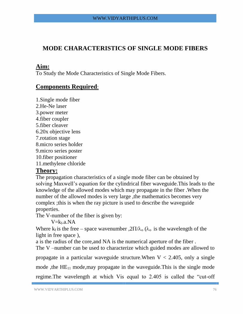
MODE CHARACTERISTICS OF SINGLE MODE FIBERS
Aim: To Study the Mode Characteristics of Single Mode Fibers.
Components Required:
1.Single mode fiber
2.He-Ne laser
3.power meter
4.fiber coupler
5.fiber cleaver
6.20x objective lens
7.rotation stage
8.micro series holder
9.micro series poster
10.fiber positioner
11.methylene chloride
Theory: The propagation characteristics of a single mode fiber can be obtained by
solving Maxwell’s equation for the cylindrical fiber waveguide.This leads to the
knowledge of the allowed modes which may propagate in the fiber .When the
number of the allowed modes is very large ,the mathematics becomes very
complex ;this is when the ray picture is used to describe the waveguide
properties.
The V-number of the fiber is given by:
V=kf.a.NA
Where kf is the free – space wavenumber ,2/o (o is the wavelength of the
light in free space ),
a is the radius of the core,and NA is the numerical aperture of the fiber .
The V –number can be used to characterize which guided modes are allowed to
propagate in a particular waveguide structure.When V < 2.405, only a single
mode ,the HE11 mode,may propagate in the waveguide.This is the single mode
regime.The wavelength at which Vis equal to 2.405 is called the “cut-off

WWW.VIDYARTHIPLUS.COM
WWW.VIDYARTHIPLUS.COM 77
wavelength”,(denoted by c) because that is the wavelength at which the next
higher order mode is cut off and no longer propagates.
TABULATION
Exponential Curve
CLOCKWISE ANTICLOCKWISE
Angle (Degrees) Power (m) Angle (Degrees) Power (m)
Gaussian Curve
CLOCKWISE ANTICLOCKWISE
Angle (Degrees) Power (m) Angle (Degrees) Power (m)
Result:
WWW.VIDYARTHIPLUS.COM
WWW.VIDYARTHIPLUS.COM 78
Thus the mode characteristics of the single mode fibers were studied.
FERRITE DEVICES
AIM:
To find the characteristics of ferrite device – circulator.
COMPONENTS REQUIRED:
1. Microwave source (klystron power supply)
2. Klystron Mount
3. Isolator
4. Variable Attenuator
5. Frequency meter
6. Circulator
7. Power Detector
8. Matched termination ----- 1 No
FORMULA:
1. The S – matrix of 3 – port circulator is
0 0 1
S = 1 0 0
0 1 0
WWW.VIDYARTHIPLUS.COM
WWW.VIDYARTHIPLUS.COM 79
Where
S11 = s22 = s33 = 0
S12 = s23 = s31 = 0
S21 = 20log (V2 / V1)
S13 = 20log (V1 / V3)
1. Insertion loss = 10 log (p1/p2)
2. Isolation = 10 log (p1/p3)
PROCEDURE:
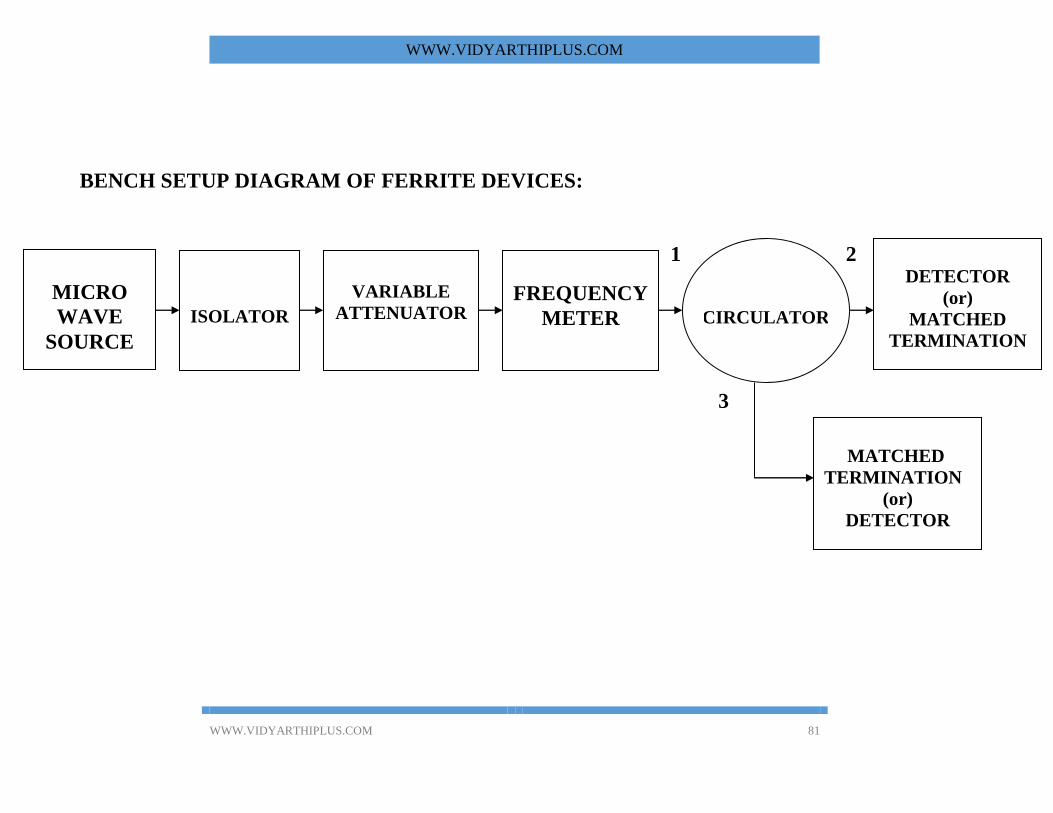
1. Arrange the bench setup with out connecting circulator
and measure the input power.
2. Now connect the circulator and note down the output
power at port 2 & port 3.
3. Substitute the values to estimate the S – matrix of
circulator.
RESULT:

WWW.VIDYARTHIPLUS.COM
WWW.VIDYARTHIPLUS.COM 80
Thus the characteristics of given 3 – port circulator was obtained and
verified.
WWW.VIDYARTHIPLUS.COM
WWW.VIDYARTHIPLUS.COM 81
BENCH SETUP DIAGRAM OF FERRITE DEVICES:
1 2
3
MICRO
WAVE
SOURCE
ISOLATOR
VARIABLE
ATTENUATOR
FREQUENCY
METER
DETECTOR
(or)
MATCHED
TERMINATION
CIRCULATOR
MATCHED
TERMINATION
(or)
DETECTOR
WWW.VIDYARTHIPLUS.COM
WWW.VIDYARTHIPLUS.COM 82
CHARACTERISTICS OF MAGIC TEE, E-PLANE AND H-PLANE TEE
AIM:
To find the characteristics of given Magic – Tee,E-plane and H-plane
COMPONENTS REQUIRED:
1. Micro wave source(klystron power supply)
2. Klystron Mount
3. Isolator
4. Variable Attenuator
5. Frequency meter
6. Magic – Tee
7. Power Detector
8. Matched termination ----- 2 No’s
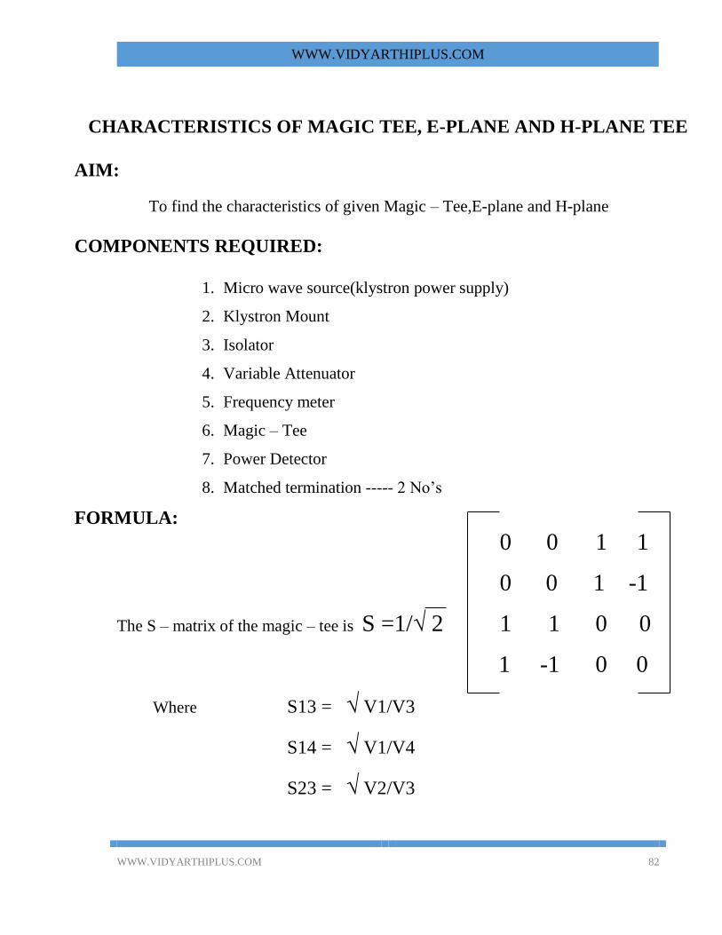
FORMULA:
0 0 1 1
0 0 1 -1
The S – matrix of the magic – tee is S =1/√ 2 1 1 0 0
1 -1 0 0
Where S13 = √ V1/V3
S14 = √ V1/V4
S23 = √ V2/V3
WWW.VIDYARTHIPLUS.COM
WWW.VIDYARTHIPLUS.COM 83
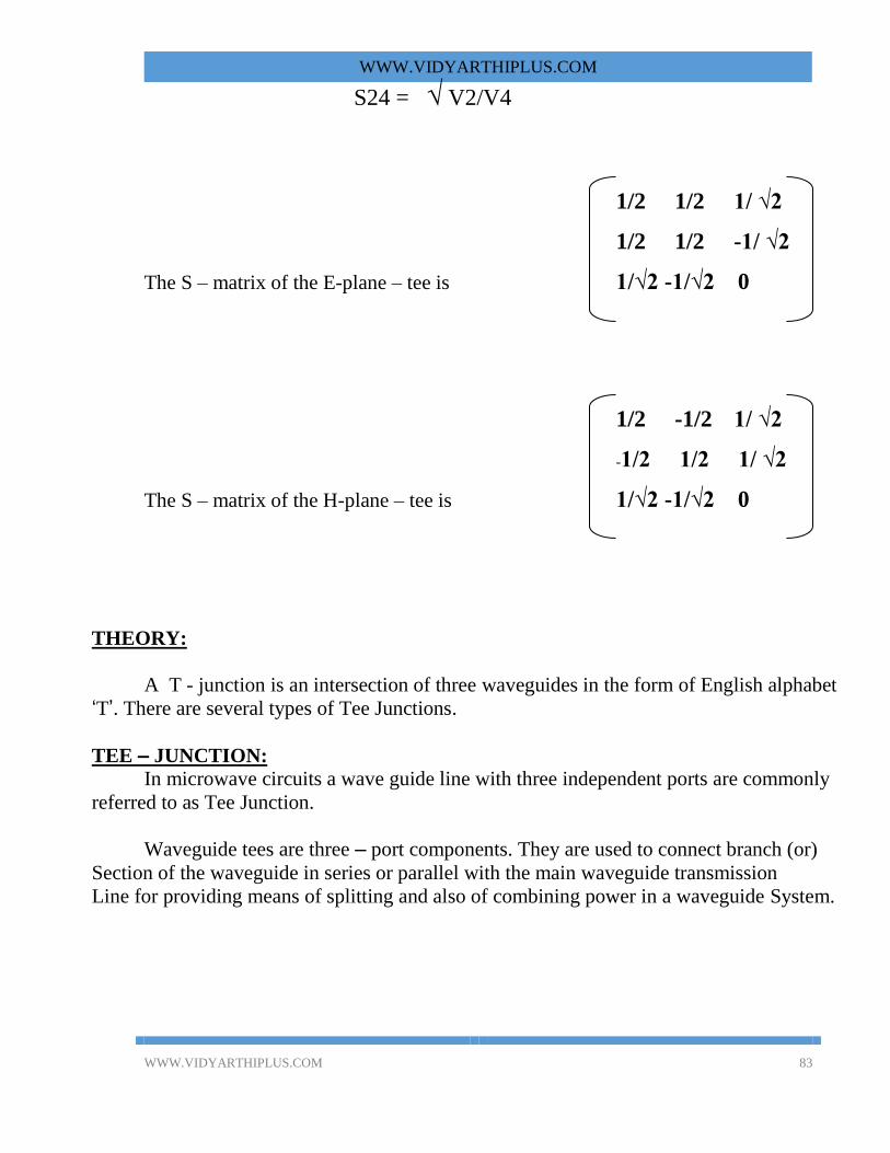
S24 = √ V2/V4
1/2 1/2 1/ √2
1/2 1/2 -1/ √2
The S – matrix of the E-plane – tee is 1/√2 -1/√2 0
1/2 -1/2 1/ √2
-1/2 1/2 1/ √2
The S – matrix of the H-plane – tee is 1/√2 -1/√2 0
THEORY:
A T - junction is an intersection of three waveguides in the form of English alphabet
‘T’. There are several types of Tee Junctions.
TEE – JUNCTION:
In microwave circuits a wave guide line with three independent ports are commonly
referred to as Tee Junction.
Waveguide tees are three – port components. They are used to connect branch (or)
Section of the waveguide in series or parallel with the main waveguide transmission
Line for providing means of splitting and also of combining power in a waveguide System.

WWW.VIDYARTHIPLUS.COM
WWW.VIDYARTHIPLUS.COM 84
H-PLANE TEE
E-PLANE TEE
WWW.VIDYARTHIPLUS.COM
WWW.VIDYARTHIPLUS.COM 85
MAGIC TEE (HYBRID OR E – H PLANE TEES)

WWW.VIDYARTHIPLUS.COM
WWW.VIDYARTHIPLUS.COM 86
The
basic types are
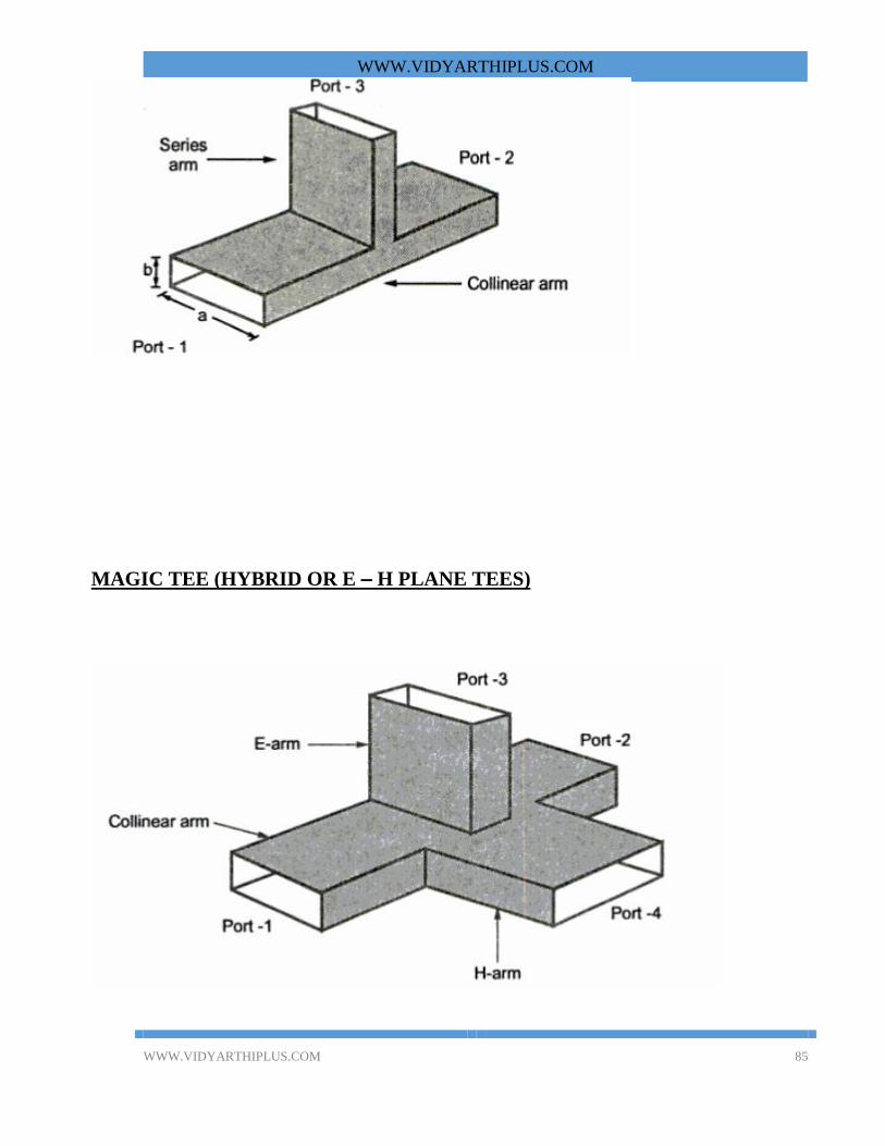
1. E – Plane Tee (series)
2. H - Plane Tee (shunt)
3. Magic Tees (Hybrid or E-H plane Tees).
E – PLANE TEE:
An E – plane tee is a waveguide tee in which the axis of its side arm is parallel to the E
– field of the main guide. A rectangular slot is cut along the broader dimension of a Long
waveguide and side arm is attached. Ports 1 and 2 are the collinear arms and port 3 is the E-
arm.
When the waves are fed into the side arm (port 3), the waves appearing at port 1 and
Port 2 of the collinear arm will be in opposite phase and in the same magnitude. If two input
waves are fed into port 1 and port 2 of the collinear arm, the output Wave at 3 will be opposite
in phase and subtractive. Hence it is called difference Arm
H – PLANE TEE:
An H –Plane Tee junction is formed by cutting a rectangular slot along width of a main
waveguide and attaching another waveguide, the side arm is called the H-arm. Ports 1 and 2
are the collinear arms and port 3 is the H- arm.
If two input waves are fed into port 1 and port 2 of the collinear arm, the output wave at
port 3 will be in phase and additive. Because of this, the third port is called the sum Arm. All
three arms of H – Plane tee lie in the plane of magnetic field, the magnetic field itself into the
arms. This is also called as current junction.
MAGIC TEES (HYBRID OR E – H PLANE TEES):
Here rectangular slots are cut both along the width and breadth of a long waveguide and
side arms are attached. Ports 1 and 2 are collinear arms, port 3 is the H- arm, and port 4 is the
E- arm. So Magic tee is the combinations of E and H Plane Tee.
A wave incident at port 3 (E –arm) divides equally between ports 1 and 2 but opposite
in phase with no coupling to port (H-ram).
A wave fed into collinear port 1 or 2 will not appear in the other collinear port 2 or 1.
Hence two collinear ports 1 and 2 are isolated from each other.

WWW.VIDYARTHIPLUS.COM
WWW.VIDYARTHIPLUS.COM 87
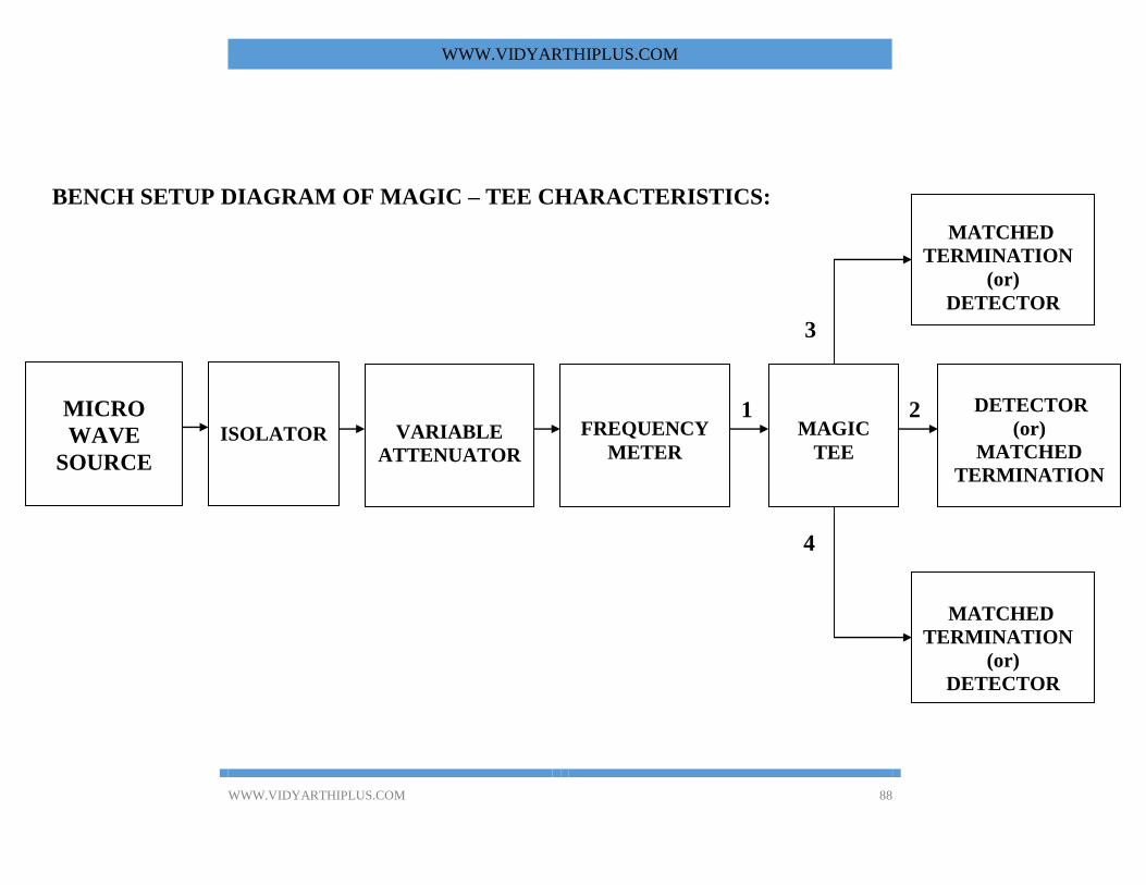
PROCEDURE:
1. Arrange the bench setup with out connecting magic – tee/E-plane/
H-Plane and measure the input power.
2. Now connect the Tee junctions and note down the output power
at port 2, port 3 & port 4.
3. Substitute the value of the port currents to obtain the scattering
parameters of given magic – tee.
3. For various values of input power find the scattering matrix.
RESULT:
Thus the characteristics of given Magic – Tee was found and verified.
WWW.VIDYARTHIPLUS.COM
WWW.VIDYARTHIPLUS.COM 88
BENCH SETUP DIAGRAM OF MAGIC – TEE CHARACTERISTICS:
3
1 2
4
MICRO
WAVE
SOURCE
ISOLATOR
VARIABLE
ATTENUATOR
MATCHED
TERMINATION
(or)
DETECTOR
DETECTOR
(or)
MATCHED
TERMINATION
MATCHED
TERMINATION
(or)
DETECTOR
FREQUENCY
METER
MAGIC
TEE
WWW.VIDYARTHIPLUS.COM
WWW.VIDYARTHIPLUS.COM 89
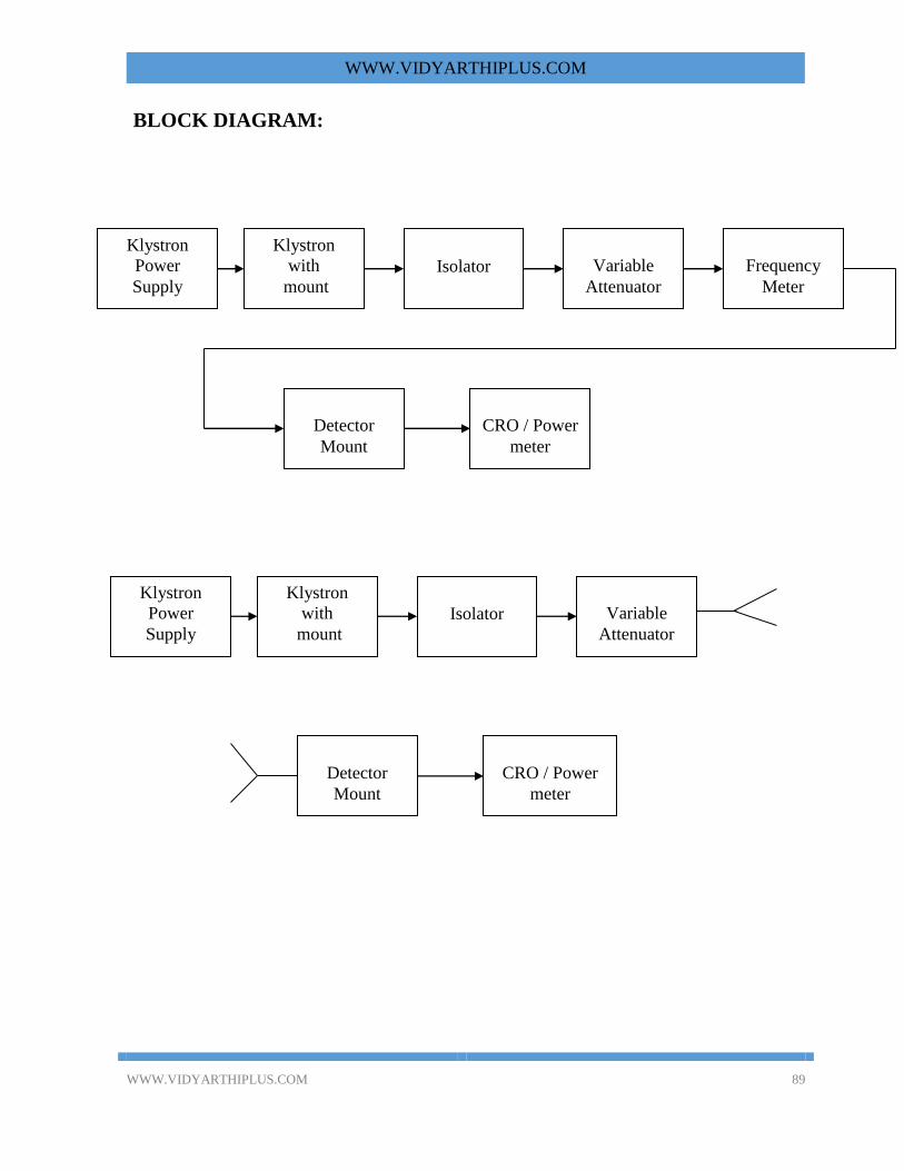
BLOCK DIAGRAM:
Klystron
Power
Supply
Klystron
with
mount
Isolator
Variable
Attenuator
Frequency
Meter
Detector
Mount
CRO / Power
meter
Klystron
Power
Supply
Klystron
with
mount
Isolator
Variable
Attenuator
Detector
Mount
CRO / Power
meter
WWW.VIDYARTHIPLUS.COM
WWW.VIDYARTHIPLUS.COM 90
ANTENNA GAIN MEASUREMENT
Aim : To find the antenna gain using two-antenna method.
Apparatus/Components Required :
1. Klystron Power supply 2. Klystron with mount
3. Isolator 4. Variable Attenuator
5. Horn Antenna[2 nos] 6. Detector Mount
7. CRO 8. Probes
9. Cooling Fan 10. Stands. 11. Power meter
Theory :
Gain as a parameter measures the directionality of a given antenna. An
antenna with a low gain emits radiation in all directions equally, whereas a
high-gain antenna will preferentially radiate in particular directions.
Specifically, the Gain or Power gain of an antenna is defined as the ratio of
the intensity (power per unit surface) radiated by the antenna in a given
direction at an arbitrary distance divided by the intensity radiated at the same
distance by an hypothetical isotropic antenna:
Precautions :
1. Before switching ON the Klystron power supply ensure that the beam
voltage knob is in the minimum position[Left extreme] and the repeller
voltage knob is in the maximum position[right extreme].
2.While doing the experiment ensure that the beam voltage and beam current
do not exceed 250 Volts and 20 mA respectively.
3.Before switching OFF the Klystron power supply ensure that the beam
voltage knob is in the minimum position[Left extreme] and the repeller
voltage knob is in the maximum position[right extreme].
WWW.VIDYARTHIPLUS.COM
WWW.VIDYARTHIPLUS.COM 91
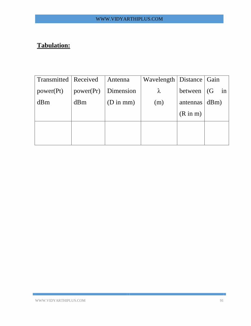
Tabulation:
Transmitted
power(Pt)
dBm
Received
power(Pr)
dBm
Antenna
Dimension
(D in mm)
Wavelength
λ
(m)
Distance
between
antennas
(R in m)
Gain
(G in
dBm)
WWW.VIDYARTHIPLUS.COM
WWW.VIDYARTHIPLUS.COM 92
Procedure :
1. Obtain square wave output without the antenna in the set-up and maximize
the output by adjusting beam voltage, repeller voltage, modulating
amplitude and note down the power(Pt)
2. Now connect the two horn antenna in the set-up and align the two antenna
both vertically and horizontally for maximum output. Ensure a minimum
distance(end to end) of (2D2/λ). Where D is the maximum dimension of
antenna.
3. Note the distance between two antennas(R).
4. Note the power received(Pr) in the power meter.
5. Calculate the gain using following formula
G=1/2(Pr-Pt-20log10(λ/4ΠR))
Result
Thus the gain of the antenna is found as ___________