+ CS 325: CS Hardware and Software Organization and Architecture Sequential Circuits 1.
22
+ CS 325: CS Hardware and Software Organization and Architecture Sequential Circuits 1
-
Upload
dayton-devereaux -
Category
Documents
-
view
221 -
download
0
Transcript of + CS 325: CS Hardware and Software Organization and Architecture Sequential Circuits 1.

+ CS 325: CS Hardware and SoftwareOrganization and Architecture
Sequential Circuits 1

+Outline
Sequential Circuits Overview
Clock Signals
Classification of Sequential Circuits
Latches/Flip Flops
S-R Latch
S-R Flip Flop
D Flip Flop
J-K Flip Flop

+Sequential Circuits
Unlike Combinational Circuits, Sequential Circuits have some form of inherent “Memory” as they are able to take into account their previous input state, as well as their current input state. Output of Sequential Circuits based on three states:
Present input state Previous input state And/Or previous output state

+Sequential Circuits
Sequential Circuits stay fixed in their current state until the next clock cycle signal changes in one of the states.

+Clock Signals
Clock: A circuit that emits a series of pulses with precise pulse
width (how long the pulse lasts) and interval (how long until the next pulse).
Number of pulses per second is the Clock Frequency, commonly between 1 and 4 billion pulses per second (1 – 4 GHz).
Clock frequency is controlled by a crystal oscillator. Time between edges of 2 consecutive pulses is the clock
cycle time. Clock frequency = 1 / clock cycle time

+Sequential Circuit Representation

+Sequential Circuits
“Sequential” means actions occur one after the other.
In sequential circuits, the clock signal determines when actions occur.
In the same way that gates are the building blocks of combinational circuits, latches and flip-flops are the building blocks of sequential circuits.
Latches and flip-flops are circuit elements whose output depends on current inputs and previous input and output states.

+Classification of Sequential Circuits

+Classification of Sequential Circuits
Event Driven: Asynchronous circuits that change state immediately when enabled. Ex: Latch
Clock Driven: Synchronous circuits that are synchronized to a specific clock signal. EX: Flip-Flop
Pulse Driven: Combination of Event and Clock driven sequential circuits that responds to triggering pulses.
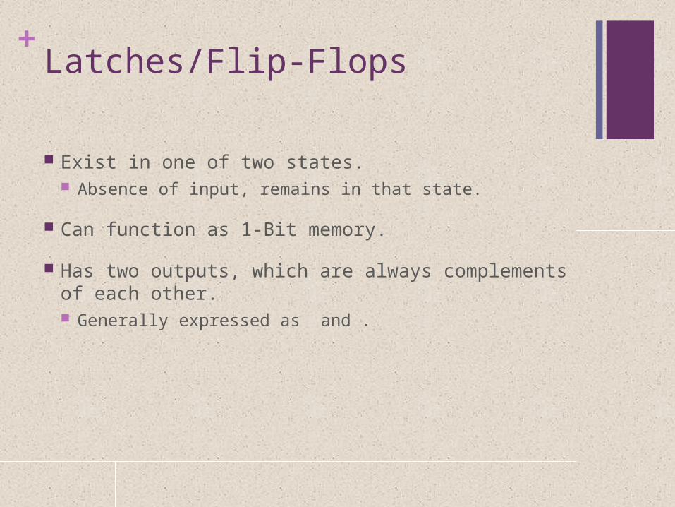
+Latches/Flip-Flops
Exist in one of two states. Absence of input, remains in that state.
Can function as 1-Bit memory.
Has two outputs, which are always complements of each other. Generally expressed as and .

+S–R Latch
Level triggered, asynchronous
Two inputs: Set, Reset
Has feedback so output Q not determined by just the 2 inputs.
Two stable states for R = S = 0. 0 or 1 depending on Q

+S–R Latch
Two stable states:
S momentarily set to 1 R momentarily set to 1
Q = 1 Q = 0

+S–R Latch Memory
Q is the value of the bit. Setting S = 1 (R remains 0) sets the value of Q to 1.
State is stable even if S is returned to 0. Setting R = 1 (S remains 0) sets the value of Q to 0.
State is stable even if R is returned to 0.
State Q = 1
State Q = 0

+S–R Latch Definition
State Table Simplified State Table
Current Inputs
Current State
Next State
S R Qn Qn+1
0 0 0 0
0 0 1 1
0 1 0 0
0 1 1 0
1 0 0 1
1 0 1 1
1 1 0 X
1 1 1 X
S R Qn+1
0 0 Qn
0 1 0
1 0 1
1 1 X
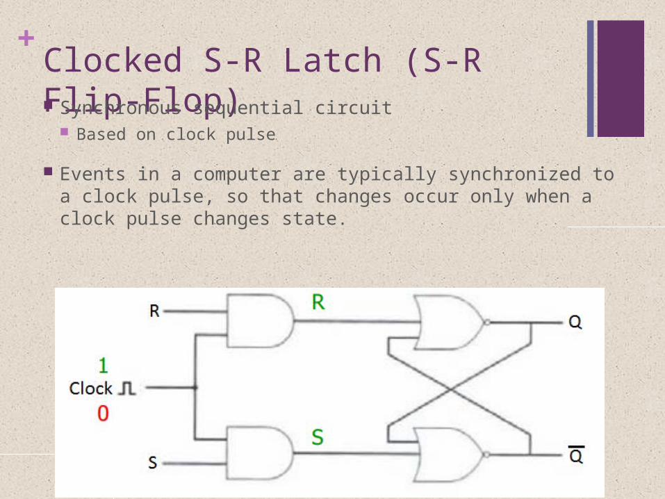
+Clocked S-R Latch (S-R Flip-Flop) Synchronous sequential circuit
Based on clock pulse
Events in a computer are typically synchronized to a clock pulse, so that changes occur only when a clock pulse changes state.
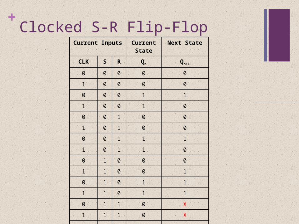
+Clocked S-R Flip-Flop
Current Inputs Current State
Next State
CLK S R Qn Qn+1
0 0 0 0 0
1 0 0 0 0
0 0 0 1 1
1 0 0 1 0
0 0 1 0 0
1 0 1 0 0
0 0 1 1 1
1 0 1 1 0
0 1 0 0 0
1 1 0 0 1
0 1 0 1 1
1 1 0 1 1
0 1 1 0 X
1 1 1 0 X
0 1 1 1 X
1 1 1 1 X

+S-R Flip-Flop Block Diagram

+D Flip-Flop Synchronous sequential circuit
Based on clock pulse
Disadvantage of S-R Flip-Flop: Set and Rest can both be set to logical “1”, resulting in (not allowed).
D Flip-Flop fixes this issue by requiring only one input D, which is connected to S, and is connected to R.

+D Flip-Flop Like clocked S-R Flip-Flop, but S = R = 1 is not possible.
Inputs S and R replaced with which will never be the same. When D is 1, Q is 1. When D is 0, Q is 0.
D Qn+1
0 0
1 1

+D Flip-Flop Block Diagram

+D Flip-Flop Uses One main use of a D Flip-Flop is as a Frequency Divider.
If the output on a D Flip-Flop is connected directly to the D input giving the device closed loop “feedback”, successive clock pulses will make the D Flip-Flop “toggle” once every two clock cycles.

+J-K Flip-Flop Synchronous sequential circuit
Based on clock pulse
The J-K Flip Flop is the most widely used of all flip-flop designs. The sequential operation is exactly the same as for the S-R Flip
Flop. The difference is the J-K Flip Flop has no invalid or forbidden input
states.J K Qn+1
0 0 Qn
0 1 0
1 0 1
1 1