Contentsweb.stanford.edu/class/ee152/resources/ee152_notes.pdf · Contents 1 Introduction: The...
230
Contents 1 Introduction: The World Needs Green Electronics 7 1.1 The Energy Crisis .......................... 7 1.2 Green Electronics: Part of the Solution .............. 8 1.2.1 Example 1: Photovoltaic Generation ............ 8 1.2.2 Example 2: An Electric Car ................. 10 1.3 The World Needs More Green Engineers .............. 11 1.3.1 Organization of this Book .................. 12 1.4 Bibliographic Notes .......................... 12 2 The Buck Converter 15 2.1 Converter Efficiency ......................... 15 2.2 Buck Topology ............................ 17 3 Analysis of the Buck Converter 21 3.1 Single-Cycle Analysis ......................... 21 3.2 Low-Frequency Analysis ....................... 23 3.3 Exercises ............................... 24 4 Simulation of the Buck Converter 25 4.1 High-Frequency Model ........................ 25 4.2 Low-Frequency Model ........................ 29 4.3 Exercises ............................... 29 5 Controlling the Buck Converter 31 5.1 Controller Derivation ......................... 31 5.2 Controller Simulation ........................ 34 5.3 Exercises ............................... 36 6 Boost and Buck-Boost Converters 37 6.1 Boost Converter ........................... 37 6.2 Buck-Boost Converter ........................ 39 6.3 Exercises ............................... 41 1
Transcript of Contentsweb.stanford.edu/class/ee152/resources/ee152_notes.pdf · Contents 1 Introduction: The...

Contents
1 Introduction: The World Needs Green Electronics 71.1 The Energy Crisis . . . . . . . . . . . . . . . . . . . . . . . . . . 71.2 Green Electronics: Part of the Solution . . . . . . . . . . . . . . 8
1.2.1 Example 1: Photovoltaic Generation . . . . . . . . . . . . 81.2.2 Example 2: An Electric Car . . . . . . . . . . . . . . . . . 10
1.3 The World Needs More Green Engineers . . . . . . . . . . . . . . 111.3.1 Organization of this Book . . . . . . . . . . . . . . . . . . 12
1.4 Bibliographic Notes . . . . . . . . . . . . . . . . . . . . . . . . . . 12
2 The Buck Converter 152.1 Converter Efficiency . . . . . . . . . . . . . . . . . . . . . . . . . 152.2 Buck Topology . . . . . . . . . . . . . . . . . . . . . . . . . . . . 17
3 Analysis of the Buck Converter 213.1 Single-Cycle Analysis . . . . . . . . . . . . . . . . . . . . . . . . . 213.2 Low-Frequency Analysis . . . . . . . . . . . . . . . . . . . . . . . 233.3 Exercises . . . . . . . . . . . . . . . . . . . . . . . . . . . . . . . 24
4 Simulation of the Buck Converter 254.1 High-Frequency Model . . . . . . . . . . . . . . . . . . . . . . . . 254.2 Low-Frequency Model . . . . . . . . . . . . . . . . . . . . . . . . 294.3 Exercises . . . . . . . . . . . . . . . . . . . . . . . . . . . . . . . 29
5 Controlling the Buck Converter 315.1 Controller Derivation . . . . . . . . . . . . . . . . . . . . . . . . . 315.2 Controller Simulation . . . . . . . . . . . . . . . . . . . . . . . . 345.3 Exercises . . . . . . . . . . . . . . . . . . . . . . . . . . . . . . . 36
6 Boost and Buck-Boost Converters 376.1 Boost Converter . . . . . . . . . . . . . . . . . . . . . . . . . . . 376.2 Buck-Boost Converter . . . . . . . . . . . . . . . . . . . . . . . . 396.3 Exercises . . . . . . . . . . . . . . . . . . . . . . . . . . . . . . . 41
1

2 Green Electronics
7 Analysis and Control of the Boost Converter 437.1 Analysis of the Boost Converter . . . . . . . . . . . . . . . . . . . 437.2 Layered Control of the Boost . . . . . . . . . . . . . . . . . . . . 457.3 Simulation . . . . . . . . . . . . . . . . . . . . . . . . . . . . . . . 477.4 Exercises . . . . . . . . . . . . . . . . . . . . . . . . . . . . . . . 47
8 Small-Signal Analysis of the Boost Converter 518.1 Impulse Response . . . . . . . . . . . . . . . . . . . . . . . . . . . 518.2 Small-Signal Model . . . . . . . . . . . . . . . . . . . . . . . . . . 538.3 Controller Design . . . . . . . . . . . . . . . . . . . . . . . . . . . 558.4 Exercises . . . . . . . . . . . . . . . . . . . . . . . . . . . . . . . 55
9 Analysis and Control of the Buck-Boost Converter 599.1 Analysis of the Buck-Boost Converter . . . . . . . . . . . . . . . 59
10 Isolated Converters 6110.1 The Ideal Transformer . . . . . . . . . . . . . . . . . . . . . . . . 6110.2 A Real Transformer . . . . . . . . . . . . . . . . . . . . . . . . . 6510.3 A Full-Bridge Converter . . . . . . . . . . . . . . . . . . . . . . . 6710.4 Effect of Leakage Inductance . . . . . . . . . . . . . . . . . . . . 7010.5 Final Comments . . . . . . . . . . . . . . . . . . . . . . . . . . . 7210.6 Exercises . . . . . . . . . . . . . . . . . . . . . . . . . . . . . . . 73
11 The Flyback Converter 7511.1 Flyback Topology and Operation . . . . . . . . . . . . . . . . . . 7511.2 Effect of Leakage Inductance . . . . . . . . . . . . . . . . . . . . 7811.3 Diagonal Flyback . . . . . . . . . . . . . . . . . . . . . . . . . . . 8011.4 Primary-Side Sensing . . . . . . . . . . . . . . . . . . . . . . . . . 8211.5 Exercises . . . . . . . . . . . . . . . . . . . . . . . . . . . . . . . 82
12 Other Isolated Converters 83
13 Discontinuous Conduction Mode 8513.1 The Buck Converter Operating in DCM . . . . . . . . . . . . . . 8613.2 Simulation . . . . . . . . . . . . . . . . . . . . . . . . . . . . . . . 8713.3 Control . . . . . . . . . . . . . . . . . . . . . . . . . . . . . . . . 8713.4 Exercises . . . . . . . . . . . . . . . . . . . . . . . . . . . . . . . 91
14 Capacitive Converters 9314.1 A Capacitive Voltage Doubler . . . . . . . . . . . . . . . . . . . . 9314.2 Analysis of the Capacitive Voltage Doubler . . . . . . . . . . . . 9414.3 Exercises . . . . . . . . . . . . . . . . . . . . . . . . . . . . . . . 96
15 Inverters 9715.1 Basic Inverter . . . . . . . . . . . . . . . . . . . . . . . . . . . . . 9715.2 Inverter Simulation . . . . . . . . . . . . . . . . . . . . . . . . . . 9815.3 Exercises . . . . . . . . . . . . . . . . . . . . . . . . . . . . . . . 102

Copyright (c) 2011-14 by W.J Dally, all rights reserved 3
16 Power Factor Correction 10316.1 Power Factor . . . . . . . . . . . . . . . . . . . . . . . . . . . . . 10316.2 Power Factor Correction . . . . . . . . . . . . . . . . . . . . . . . 10516.3 Simulation of a PFC Input Stage . . . . . . . . . . . . . . . . . . 10616.4 A Grid-Tied Inverter . . . . . . . . . . . . . . . . . . . . . . . . . 10616.5 Three-Phase Systems . . . . . . . . . . . . . . . . . . . . . . . . . 10616.6 Exercises . . . . . . . . . . . . . . . . . . . . . . . . . . . . . . . 106
17 Switches 10917.1 DC Characteristics of Real Switches . . . . . . . . . . . . . . . . 10917.2 AC Characteristics of FETs and IGBTs . . . . . . . . . . . . . . 111
18 Metal-Oxide Field Effect Transistors (MOSFETs) 11518.1 Simple Model . . . . . . . . . . . . . . . . . . . . . . . . . . . . . 11518.2 Structure . . . . . . . . . . . . . . . . . . . . . . . . . . . . . . . 11618.3 Dynamics . . . . . . . . . . . . . . . . . . . . . . . . . . . . . . . 11918.4 Parasitic Elements . . . . . . . . . . . . . . . . . . . . . . . . . . 11918.5 Avalanche Energy . . . . . . . . . . . . . . . . . . . . . . . . . . 12218.6 Typical MOSFETs . . . . . . . . . . . . . . . . . . . . . . . . . . 12218.7 Exercises . . . . . . . . . . . . . . . . . . . . . . . . . . . . . . . 122
19 Diodes 12319.1 Simple Model . . . . . . . . . . . . . . . . . . . . . . . . . . . . . 12419.2 Key Parameters . . . . . . . . . . . . . . . . . . . . . . . . . . . . 12619.3 Reverse Recovery . . . . . . . . . . . . . . . . . . . . . . . . . . . 12819.4 Forward Recovery . . . . . . . . . . . . . . . . . . . . . . . . . . 13319.5 Current Hogging . . . . . . . . . . . . . . . . . . . . . . . . . . . 13519.6 SPICE Models . . . . . . . . . . . . . . . . . . . . . . . . . . . . 13919.7 Measurements . . . . . . . . . . . . . . . . . . . . . . . . . . . . . 14019.8 Exercises . . . . . . . . . . . . . . . . . . . . . . . . . . . . . . . 140
20 Switch Pairs 143
21 Anatomy of a Switching Cycle 14521.1 An IGBT Half-Bridge . . . . . . . . . . . . . . . . . . . . . . . . 14521.2 A Switching Cycle . . . . . . . . . . . . . . . . . . . . . . . . . . 14721.3 High-Side Turn-On . . . . . . . . . . . . . . . . . . . . . . . . . . 14821.4 High-Side Turn Off . . . . . . . . . . . . . . . . . . . . . . . . . . 15021.5 Reverse Current . . . . . . . . . . . . . . . . . . . . . . . . . . . 150
22 Gate Drive 151
23 Magnetic Components 15323.1 Magnetic Circuits . . . . . . . . . . . . . . . . . . . . . . . . . . . 15323.2 Equivalent Magnetic Circuits . . . . . . . . . . . . . . . . . . . . 15623.3 Inductance . . . . . . . . . . . . . . . . . . . . . . . . . . . . . . 15923.4 Transformers . . . . . . . . . . . . . . . . . . . . . . . . . . . . . 160

4 Green Electronics
23.5 Exercises . . . . . . . . . . . . . . . . . . . . . . . . . . . . . . . 163
24 Magnetic Materials 16524.1 Magnetic Materials . . . . . . . . . . . . . . . . . . . . . . . . . . 165
24.1.1 Saturation . . . . . . . . . . . . . . . . . . . . . . . . . . . 16524.1.2 Hysteresis . . . . . . . . . . . . . . . . . . . . . . . . . . . 166
24.2 Exercises . . . . . . . . . . . . . . . . . . . . . . . . . . . . . . . 170
25 Wire for Magnetics 17125.1 Skin Effect . . . . . . . . . . . . . . . . . . . . . . . . . . . . . . 17125.2 Proximity Effect . . . . . . . . . . . . . . . . . . . . . . . . . . . 17225.3 Litz Wire . . . . . . . . . . . . . . . . . . . . . . . . . . . . . . . 17225.4 Winding Geometry . . . . . . . . . . . . . . . . . . . . . . . . . . 17225.5 Exercises . . . . . . . . . . . . . . . . . . . . . . . . . . . . . . . 173
26 Designing Magnetic Components 17526.1 Inductor Design . . . . . . . . . . . . . . . . . . . . . . . . . . . . 17526.2 Inductor Example . . . . . . . . . . . . . . . . . . . . . . . . . . 17626.3 Transformer Design . . . . . . . . . . . . . . . . . . . . . . . . . . 17626.4 Exercises . . . . . . . . . . . . . . . . . . . . . . . . . . . . . . . 176
27 Electric Motors 17927.1 Lorentz Force and Faraday Induction . . . . . . . . . . . . . . . . 17927.2 The Brushed Permanent Magnet Motor . . . . . . . . . . . . . . 18127.3 Motor Model . . . . . . . . . . . . . . . . . . . . . . . . . . . . . 18227.4 The Torque Curve . . . . . . . . . . . . . . . . . . . . . . . . . . 18327.5 Step Response . . . . . . . . . . . . . . . . . . . . . . . . . . . . 18527.6 Motor Drive . . . . . . . . . . . . . . . . . . . . . . . . . . . . . . 18727.7 Exercises . . . . . . . . . . . . . . . . . . . . . . . . . . . . . . . 189
28 Motor Control 19128.1 A Naive Controller . . . . . . . . . . . . . . . . . . . . . . . . . . 19128.2 PI Motor Control . . . . . . . . . . . . . . . . . . . . . . . . . . . 19328.3 Current-Limited Control . . . . . . . . . . . . . . . . . . . . . . . 19328.4 Exercises . . . . . . . . . . . . . . . . . . . . . . . . . . . . . . . 196
29 Brushless Permanent Magnet Motors 19729.1 Motor Geometry . . . . . . . . . . . . . . . . . . . . . . . . . . . 197
29.1.1 Back EMF . . . . . . . . . . . . . . . . . . . . . . . . . . 19929.1.2 Torque . . . . . . . . . . . . . . . . . . . . . . . . . . . . . 199
29.2 Equivalent Circuit . . . . . . . . . . . . . . . . . . . . . . . . . . 20129.3 Brushless Motor Drive . . . . . . . . . . . . . . . . . . . . . . . . 20129.4 Hard Electronic Commutation . . . . . . . . . . . . . . . . . . . . 20329.5 Excercises . . . . . . . . . . . . . . . . . . . . . . . . . . . . . . . 203

Copyright (c) 2011-14 by W.J Dally, all rights reserved 5
30 AC Induction Motors 20530.1 Motor Geometry . . . . . . . . . . . . . . . . . . . . . . . . . . . 20530.2 Induction Motor Operation . . . . . . . . . . . . . . . . . . . . . 20530.3 Equivalent Circuit . . . . . . . . . . . . . . . . . . . . . . . . . . 20930.4 Induction Motor Control . . . . . . . . . . . . . . . . . . . . . . . 21030.5 Exercises . . . . . . . . . . . . . . . . . . . . . . . . . . . . . . . 215
31 Soft Switching 21931.1 The Quasi-Square-Wave Converter . . . . . . . . . . . . . . . . . 21931.2 Control of the Quasi-Square-Wave Converter . . . . . . . . . . . 22531.3 Exercises . . . . . . . . . . . . . . . . . . . . . . . . . . . . . . . 228

6 Green Electronics

Chapter 1
Introduction: The WorldNeeds Green Electronics
1.1 The Energy Crisis
An increasing, industrialized world population is putting undue pressures onour planet’s delicate ecosystem and on our natural resources. In the UnitedStates, 85% of energy generated is from fossil fuels (DOE Annual Energy Out-look). While there are large reserves, that are increasing as people get betterat exploration and recovery, the supply is finite. We will ultimately run out offossil fuels.
Even if our supply of fossil fuels was infinite, burning fossil fuels generatesgreenhouse gasses like CO2 that accumulate in the atmosphere leading to climatechange. In recent years, atmospheric CO2 has been increasing at a rate of about20ppm/decade (5% per decade) (NOAA data). We need to burn less fossil fuels,or sequester the carbon generated by burning these fuels, or both — or sufferthe consequences of climate change.
To deal both with the limited supplies of fossil fuels and their environmentalimpact, we need to develop technologies for economic renewable energy sources.Wind and solar power are two of the most promising candidates — both dependstrongly on green electronics. Photovoltaic controllers, generator controllers,and inverters are important components in efficiently getting energy from solarcells and windmills to the grid — and ultimately to the end user.
Conservation plays a large role in reducing our consumption of fossil fuelsand our generation of greenhouse gasses. Replacing inefficient incandescentlamps with highly-efficient LED lamps and using intelligent control to havelamps only illuminate areas where people are looking can dramatically reducethe energy consumption due to lighting. Data centers, which consume about2% of the electric power in the US, use power supplies that are often only 70-80% efficient and processors that spend the bulk of their power on overhead.More efficient power supply and processor design would dramatically reduce
7

8 Green Electronics
electricity consumption. There are many more examples where efficient powerelectronics and intelligent control can greatly reduce consumption.
1.2 Green Electronics: Part of the Solution
A key technology for both sustainable energy generation and conservation isthe combination of intelligent control with power electronics — the brains andbrawn of energy systems. The power electronics provides the brawn — doingthe heavy work of converting energy from one form to another. This includeselectrical conversion — as in a photovoltaic system where the DC output voltagefrom a string of solar panels is converted to AC power at a different voltage todrive the grid — and mechanical conversion where the system includes a motoror generator — as in a wind farm or an electric vehicle.
Intelligent computer control provides the brains of the system, optimizingoperation to improve efficiency. A photovoltaic controller searches to find theoptimum operating point for each solar cell in a string — optimizing efficiency.A controller electrically switches the windings of a brushless generator on a windmill, achieving greater efficiency than with an alternator or a generator with acommutator. A lighting controller uses cameras to sense the location and gazeof people in a building to turn on lights only where they are needed.
1.2.1 Example 1: Photovoltaic Generation
As an example of a green-electronics system, consider the grid-connected photo-voltaic system of Figure 1.1. A photovoltaic (PV) array of solar panels convertssolar energy to electricity. With a typical configuration of 10 40V panels ineach series string, the output of this array is 400V DC. The power depends onthe number of strings and for a residential system is typically in the range of4-10kW. So the DC current out of the PV array is in the range of 10-25A.
A PV Controller and Inverter connects the PV array to a bank of batteries(that operate at 48V DC) and to the electric grid (240V AC). The PV controllerconverts electrical energy from one form to another. For a 4kW system, itconverts 10A at 400V DC to 16.7A at 240V AC to drive the grid, or to 83.3Aat 48V DC to charge the batteries.
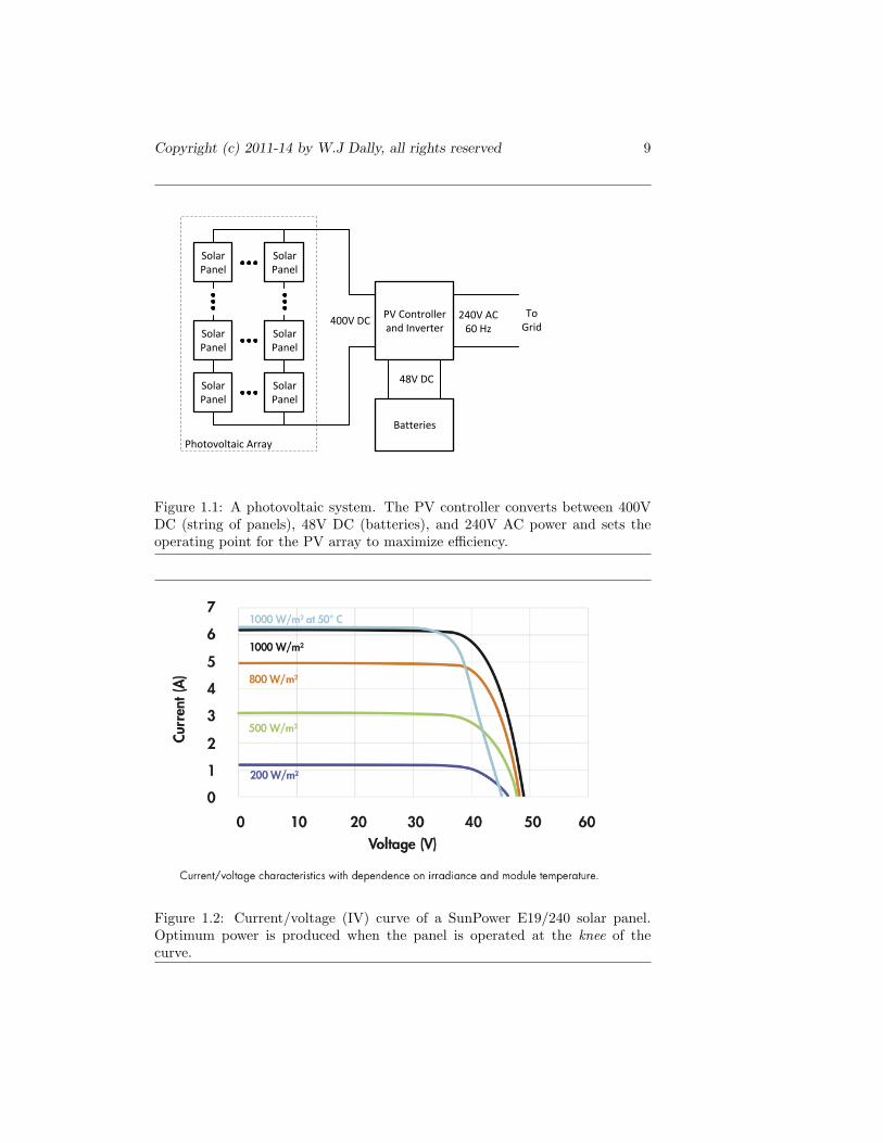
The controller also sets the operating point of the PV array to maximizethe energy produced. As shown in Figure 1.2, a solar panel acts as a currentsource — producing a nearly constant current up until a maximum voltagewhere the current falls quickly. To get maximum power out of the panel, itmust be operated at the knee of this curve — at the voltage where the currentjust begins to drop. The PV controller adjusts its output impedance to operatethe array at this point.
Because of non-uniformity of illumination and manufacturing not all panelsmay have the same opimal operating point. In a simple system like that shown inFigure 1.1 the controller must set a single operating point that is a compromise— it gives the highest power over all but may not be the best for each panel.
Copyright (c) 2011-14 by W.J Dally, all rights reserved 9
Solar Panel
Solar Panel
Solar Panel
Solar Panel
Solar Panel
Solar Panel
Photovoltaic Array
PV Controller and Inverter
Batteries
400V DC 240V AC60 Hz
48V DC
To Grid
Figure 1.1: A photovoltaic system. The PV controller converts between 400VDC (string of panels), 48V DC (batteries), and 240V AC power and sets theoperating point for the PV array to maximize efficiency.
Figure 1.2: Current/voltage (IV) curve of a SunPower E19/240 solar panel.Optimum power is produced when the panel is operated at the knee of thecurve.

10 Green Electronics
Charger120/240V AC60 Hz
From Grid
Battery
Battery
Battery
Battery Pack
400V DCMotor
Controller
AC Induction or Brushless PM Motor
400V DC
3-phase ACVariable Voltage
Variable Frequency
Resistive Load
User Interface
DC-DC Converter
12VDC to Aux Circuits
400V DC
Figure 1.3: Block diagram of an electric car. Energy is stored in a centralbattery pack that can be charged from the grid when the car is parked. Acontroller can transfer energy in either direction between the battery pack andan electric motor.
More sophisticated PV controllers monitor the voltage and current acrosseach panel independently and by bypassing current around some panels (usinga switched-inductor shunt) operate every panel at its peak power point.
In a grid-connected system that includes battery storage, an intelligent con-troller decides when to charge the batteries to make best use of time-of-daypower rates. It will charge the batteries during off-peak times when electricityis substantially cheaper than during peak times1. Not only does this optimizeeconomics, it also optimizes efficiency because the peaking plants used by theelectric utility to provide power at peak times are substantially less efficientthan the plants used to provide base capacity.
The controller will also tailor the charging profile to maximize efficiency andbattery life. A sophisticated controller will monitor the voltage of individualbattery cells and balance the cells to optimize operation.
1.2.2 Example 2: An Electric Car
A second example of a green electronics system is the electric car of Figure 1.3.The electronics here charge and manage the batteries and control the motorthat provides vehicle propulsion.
When the car is parked, a charger converts 120V or 240V AC power to 400VDC power to charge the battery pack. While individual battery cells range from2V (lead-acid) to 3.7V (Lithium ion), hundreds of these cells are connected inseries to give an efficient operating voltage of 400V DC. The charger mustcarefully manage voltage, current, and temperature during the charging processto maximize efficiency and battery life.
The motor controller converts the 400V DC voltage to a three-phase AC
1Under the California E-7 Tariff, the peak rate is nearly four times the off-peak rate.

Copyright (c) 2011-14 by W.J Dally, all rights reserved 11
voltage to drive the motor. The frequency of the motor drive depends on themotor speed. The effective voltage of the motor drive is varied using pulse-widthmodulation to control the motor current which determines the torque producedby the motor.
The motor controller employs a control law to decide how much current, andhence torque, to apply at any given time. The decision depends on throttleposition, vehicle speed, and battery state. The decision made is a compromisebetween drivability, energy efficiency, and battery longevity.
To recycle energy when slowing the car, the motor controller employs regen-erative braking by operating the motor as a generator. In this case, the kineticenergy of the vehicle is converted to electrical energy that is used to charge thebattery. During this process, the motor controller acts as a generator controller— sequencing the motor phases to optimize generator efficiency and controllingthe battery charging process. If regenerative braking occurs when the batteriesare fully charged the excess energy is disspated as thermal energy in a resistiveload.
In all modes of operation — whether accelerating or braking — the batterypack must be carefully managed to balance cell voltages, and avoid excessivecurrents and temperatures. Lithium Ion cells are particularly sensitive to properbattery management.
In a hybrid vehicle where a heat engine can be turned on to provide propul-sion and charge batteries the controller has an additional degree of freedom.The controller must decide when to turn on the heat engine, how to divide thetorque load between the heat engine and the electric motor, and how much en-ergy to divert to charging batteries when the heat engine is running. Makingoptimal power management decisions may involve predicting the future route ofthe car — for example, whether it is likely to arrive at a charging station soon,or whether it is likely to be doing up or down a large hill.
A user interface is provided to that the driver can understand how theircontrol actions result in energy movement within the system. A good userinterface can train the driver to drive more efficiently. Of course one must becareful with the user interface to avoid distracting the driver2
1.3 The World Needs More Green Engineers
To realize green electronic systems like efficient photovoltaic controllers, windmill controllers, energy converters, electric- and hybrid-vehicle drives, etc... re-quires engineers who understand power electronics and computer control. Thereis a shortage of such talented individuals.
The goal of this course is to teach the basics of these two critical disciplinesas an introductory engineering course. The course teaches engineering thinkingusing green electronic examples. In doing so, it conveys engineering fundamen-tals — learning the process of specification, design, and analysis and learning
2In the long run the computer will drive the car, resulting in more efficient operation.

12 Green Electronics
techniques like modeling and simulation. At the same time, it gives a workingknowledge of simple power electronics and microprocessor-based control.
1.3.1 Organization of this Book
This book is organized into four parts. Chapters 2 to 16 describes the toopology,analysis, and control of voltage converters. As evidenced by our photovoltaicand electric car examples above, such converters are central to all Green Elec-tronics systems. These converters are realized from semiconductor switches(MOSFETs, IGBTs, and diodes) and magnetic components. The propertiesand design of these components and their uses are discussed in Chapters ??to 26. The motors that are used to convert between electrical and mechanicalenergy are covered in Chapters 27 to ??. The control systems that are used tocontrol both voltage converters and motors are described in Chapters ?? to ??.
1.4 Bibliographic Notes
DOE Annual Energy Outlook NOAA data

Copyright (c) 2011-14 by W.J Dally, all rights reserved 13
Part I. Voltage ConvertersBuck converterBuck AnalysisBuck SimulationBuck ControlNon-Isolated ConvertersIsolated convertersFlybackDiscontinuous mode Capacitive convertersInvertersPower Factor and PFC

14 Green Electronics

Chapter 2
The Buck Converter
Efficient voltage conversion is at the core of most green-electronic systems. Con-verting power from a photovoltaic array to drive the AC line, controlling a mo-tor, and providing an efficient power supply to a computer are at their coreproblems of efficient voltage conversion. In this chapter we introduce the buckconverter which is one of the simplest and most widely used voltage converters.A simple buck regulator, for example, is used in most computer power suppliesto convert an intermediate 12V DC voltage to a 1V DC supply voltage to powerthe processor.
2.1 Converter Efficiency
As shown in Figure 2.1, a voltage converter takes an input supply with voltage V1
and supplies a load across its output with a different voltage, V2. The convertershown in Figure 2.1 is a non-isolated converter because the source and loadshare a common terminal. In Chapter 10 we will consider the design of isolatedconverters in which the input and output voltages need not be referenced to acommon point.
If the load in Figure 2.1 draws current I2, then the power delivered to theload is P2 = I2V2. If the input current is I1, then the input power is P1 = I1V1.With no energy storage or generation in our converter we must have P1 >= P2.We define the loss as
PL = P1 − P2. (2.1)
and the efficiency of the converter is given by
ν =P2
P1. (2.2)
A simple way to convert voltage levels is to drop the input voltage across aresistor as shown in Figure 2.2(a). Resistor R must be set so that R = V1−V2
I2
15

16 Green Electronics
Converter
V1 V2 Load
+
-
+
-
Figure 2.1: A voltage converter. A voltage converter accepts input voltage V1
from a voltage source and converts the source power to output voltage V2 thatis supplied to a load.
R
V1 V2 Load
+
-
+
-
Converter
V1 V2 Load
+
-
+
-
Converter
VRef
(a) (b)
Figure 2.2: A dissipative voltage converter. (a) The input voltage is reduced bydropping the difference voltage across a resistor. (b) In practice the resistor isrealized by a PFET and a feedback loop adjusts the resistance of the PFET togive the desired output voltage.
Copyright (c) 2011-14 by W.J Dally, all rights reserved 17
L
iL
VS
+
-
a
bvC Load
+
-
C iLoad
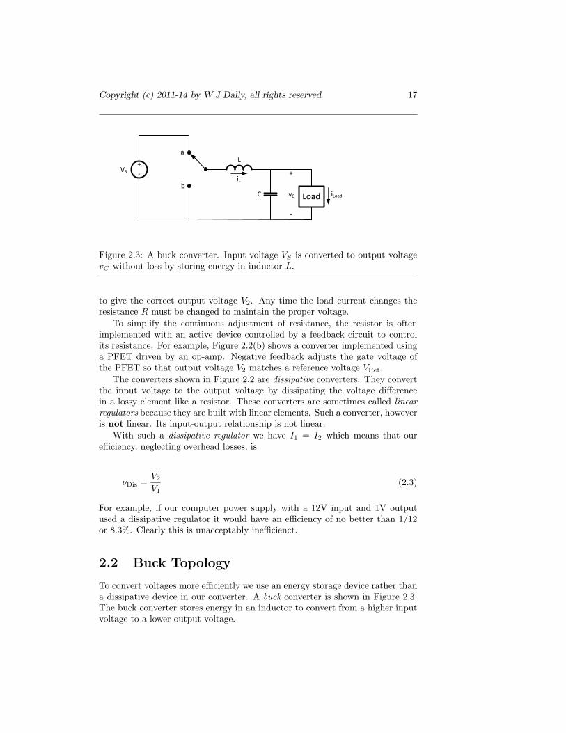
Figure 2.3: A buck converter. Input voltage VS is converted to output voltagevC without loss by storing energy in inductor L.
to give the correct output voltage V2. Any time the load current changes theresistance R must be changed to maintain the proper voltage.
To simplify the continuous adjustment of resistance, the resistor is oftenimplemented with an active device controlled by a feedback circuit to controlits resistance. For example, Figure 2.2(b) shows a converter implemented usinga PFET driven by an op-amp. Negative feedback adjusts the gate voltage ofthe PFET so that output voltage V2 matches a reference voltage VRef .
The converters shown in Figure 2.2 are dissipative converters. They convertthe input voltage to the output voltage by dissipating the voltage differencein a lossy element like a resistor. These converters are sometimes called linearregulators because they are built with linear elements. Such a converter, howeveris not linear. Its input-output relationship is not linear.
With such a dissipative regulator we have I1 = I2 which means that ourefficiency, neglecting overhead losses, is
νDis =V2
V1(2.3)
For example, if our computer power supply with a 12V input and 1V outputused a dissipative regulator it would have an efficiency of no better than 1/12or 8.3%. Clearly this is unacceptably inefficienct.
2.2 Buck Topology
To convert voltages more efficiently we use an energy storage device rather thana dissipative device in our converter. A buck converter is shown in Figure 2.3.The buck converter stores energy in an inductor to convert from a higher inputvoltage to a lower output voltage.
18 Green Electronics
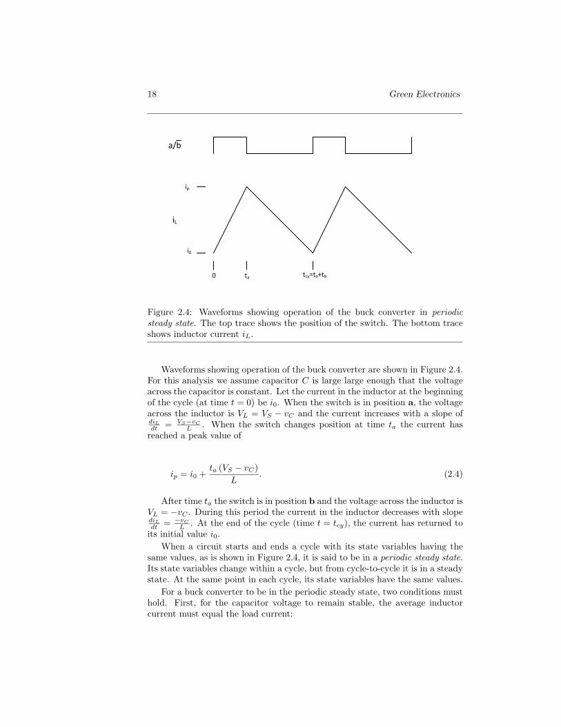
ip
i0
0 ta tcy=ta+tb
iL
a/b
Figure 2.4: Waveforms showing operation of the buck converter in periodicsteady state. The top trace shows the position of the switch. The bottom traceshows inductor current iL.
Waveforms showing operation of the buck converter are shown in Figure 2.4.For this analysis we assume capacitor C is large large enough that the voltageacross the capacitor is constant. Let the current in the inductor at the beginningof the cycle (at time t = 0) be i0. When the switch is in position a, the voltageacross the inductor is VL = VS − vC and the current increases with a slope ofdiL
dt = VS−vC
L . When the switch changes position at time ta the current hasreached a peak value of
ip = i0 +ta (VS − vC)
L. (2.4)
After time ta the switch is in position b and the voltage across the inductor isVL = −vC . During this period the current in the inductor decreases with slopediL
dt = −vC
L . At the end of the cycle (time t = tcy), the current has returned toits initial value i0.
When a circuit starts and ends a cycle with its state variables having thesame values, as is shown in Figure 2.4, it is said to be in a periodic steady state.Its state variables change within a cycle, but from cycle-to-cycle it is in a steadystate. At the same point in each cycle, its state variables have the same values.
For a buck converter to be in the periodic steady state, two conditions musthold. First, for the capacitor voltage to remain stable, the average inductorcurrent must equal the load current:

Copyright (c) 2011-14 by W.J Dally, all rights reserved 19
|iL| =i0 + ip
2= ILoad. (2.5)
Second, for the inductor current to return to i0 at the end of the cycle we musthave the volt-seconds applied to the inductor sum to zero over the cycle:
ta (VS − vC)− (tcy − ta) (vC) = 0. (2.6)
Which we can rewrite as
taVS = tcyvC (2.7)tatcy
=vC
VS
D =vC
VS(2.8)
From (2.8) we see that in the periodic steady state the voltage ratio of theconverter vC/VS is equal to the duty factor of the switch D = ta/tcy. Analysisof the converter when it is not in the periodic steady state will be covered inChapter 3.
The principle of superposition is useful in analyzing switching power circuits.A simple way to directy write (2.7) is to consider each voltage source in turn.If we zero vC and consider only VS we see that a voltage of VS is applied acrossthe inductor for duration ta. Then we zero VS and consider only vC and seethat −vC is applied across the inductor during the entire cycle tcy. Hence, thetotal volt-seconds seen by the inductor is VSta − vCtcy.
The buck converter can also be understood by considering it to be a pulsewidth modulator followed by a low-pass filter. The switch produces a voltageVx at the left terminal of the inductor with a duty factor D = ta/tcy and anamplitude of VS . Thus, the average voltage at this point is |Vx| = DVS . Theinductor and capacitor act as a low-pass filter to produce this average voltageat the output so that vC = |Vx| = DVS .
If the switch and the inductor in Figure 2.3 are ideal the converter is lossless:P2 = P1 and νBuck = 1. Unfortunately real switches have finite switching timesleading to switching losses. Also, real switches and inductors have non-zeroresistance leading to conduction losses. We will consider ideal elements for nowand revisit real losses in Chapter ??.

20 Green Electronics

Chapter 3
Analysis of the BuckConverter
Suppose the buck converter is not in periodic steady state. How do its statevariables iL and vC evolve over time as a function of duty factor D and loadcurrent iLoad? We can most easily address this question by considering twodifferent time scales. First we consider how the state variables evolve over asingle switching cycle. Then, using this relationship to determine the changein state variables over each cycle, we analyze the dynamics of the circuit atfrequencies lower than the switching frequency.
3.1 Single-Cycle Analysis
Figure 3.1 shows the inductor current for a buck converter that is not in periodicsteady state. The converter starts cycle 0 with current i0 and ramps up tocurrent ip0 as given by (2.4). However, at the end of the cycle, the current isleft at i1 6= i0, the starting current for cycle 1.
We can compute the difference current during cycle i ∆ii by considering theimbalance in volt-seconds applied to the inductor each cycle
∆ii =VSta − vitcy
L
=tcy (DVS − vi)
L. (3.1)
Here VS is the source voltage applied to the input of the circuit and vi is thevoltage across the capacitor at the start of cycle i. We continue to assume it isapproximately constant across the cycle to simplify our analysis.
The starting current for each cycle is simply this difference current added tothe starting current from the previous cycle:
21

22 Green Electronics
ip0
i0
0 ta tcy=ta+tb
iL
a/b
i1
i2
tcy+ta 2tcy
ip1
Figure 3.1: Waveforms showing operation of the buck converter when it is notin periodic steady state. The top trace shows the position of the switch. Thebottom trace shows inductor current iL.
ii+1 = ii + ∆ii. (3.2)
The peak current each cycle is given by adding the inital ramp to the startingcurrent for that cycle:
ipi = ii +ta (VS − vi)
L. (3.3)
The average current over cycle i is given by
ii =(ta
2tcy
)ii +
(12
)ipi +
(tcy − ta
2tcy
)ii+1. (3.4)
ii =12
(Dii + ipi + (1−D)ii+1) . (3.5)
To simplify analysis we will make the approximation
ii ≈12
(ii + ipi) . (3.6)
= ii +ta (VS − vi)
2L. (3.7)

Copyright (c) 2011-14 by W.J Dally, all rights reserved 23
From this average current we can calculate the change in capacitor voltage eachcycle
∆vi =tcy
(ii − iLoad
)C
(3.8)
This analysis has assumed that the voltage across the capacitor is constant,even though it is changing each cycle. For large capacitors, and hence smallvoltage changes, this approximation is valid. The full analysis, consideringthe effects of capacitor volage changes within each cycle, is considerably morecomplex. The current waveforms are not piecewise linear but rather segmentsof sine waves with frequency ω = (LC)−1/2.
The increasing current in a buck converter not in steady state shown in Fig-ure 3.1 highlights the importance of a controller that regulates the operation ofthe converter. Without a controller the current can quickly ramp to destructivelevels.
3.2 Low-Frequency Analysis
At frequencies lower than the switching frequency we are not concerned with thedetailed waveforms within each cycle, but rather only with the evolution of statevariables from cycle to cycle. Equations (3.1) and (3.8) describe the evolution ofiL and vC as a discrete-time system. We approximate these difference equationswith differential equations to give a continuous time system to simplify analysis.
di
dt=DVS − vi
L(3.9)
dv
dt=ii − iLoad
C. (3.10)
Taking the Laplace transform of (3.9) and (3.10) gives:
I(s) =D(s)VS − V (s)
Ls(3.11)
V (s) =I(s)− ILoad(s)
Cs(3.12)
Combining these gives
I(s) =D(s)VS
Ls− I(s) + ILoad(s)
LCs2
LCs2I(s) = CVSD(s)s− I(s) + ILoad(s)
I(s)(1 + LCs2) = CVsD(s)s+ ILoad(s)
I(s) =D(s)CVss+ ILoad(s)
1 + LCs2(3.13)

24 Green Electronics
Substituting (3.13) into (3.12) gives:
V (s) =D(s)Vs
1 + LCs2+ILoad(s)(1 + 1/Cs)
1 + LCs2(3.14)
If we are concerned with the transfer function from D(s) to V (s) we can (fornow) ignore ILoad and write:
V (s)D(s)
=Vs
1 + LCs2(3.15)
Equations (3.13) through (3.15) show that the response of the buck converterto a transient in D, VS , or iLoad is an undamped oscillation with frequencyω = (LC)−1/2. The denominator of I(s) has a damping factor of ζ = 0. Adissipative element, such as a resistor in series with the source, is needed todamp these oscillations, or a controller is needed to prevent them.
Even if the oscillations are damped, an overshoot of more than a few percentcan lead to destruction of the load. Consider our computer power supply. Whenthe converter turns on, a transient in D from 0 to 0.083, the output voltage willoscillate between 0 and 2V before eventually settling to 1V. The first excursionabove 1.2V is likely to do permanent damage to the load (the computer). Anytransient in load current will excite similar oscillations. A controller is requiredto prevent destructive overshoot.
In a real buck converter there are some additional components that affectthe dynamics of the system. In particular, the parasitic series resistance (ESR)of the output capacitor introduces a zero in the transfer function of (3.15). Thiszero must be taken into account when designing controllers for the buck.
3.3 Exercises
relax constant capacitor voltage approximationadd series resistor to voltage sourceadd resistive loadadd ESR to capacitorresponse to change in input voltage

Chapter 4
Simulation of the BuckConverter
We can understand the dynamics of our buck converter by building a modelthat simulates these dynamics by evolving the state variables over small timesteps. Using the simulation model we can see the open-loop response of thesystem to an input stimulus. We can also implement a control law and examinethe closed-loop response of the system with a controller.
4.1 High-Frequency Model
To simulate our system we divide time into small steps of magnitude dt andcompute the change to our state variables over each time step. We need tochoose the time step small enough to make our simulation stable and to avoidinaccuracies due to discretization of time. In practice dividing each switch-ing cycle into 100 time steps provides sufficient accuracy and gives reasonablesimulation run times.
Figure 4.1 shows Matlab code that computes the evolution of the state vari-ables iL and vC for one time step. The if statement computes the change ininductor current di l depending on the position of the switch a. This is justapplying the constituent equation of the inductor
iL =∫vL
Ldt.
Which we can rewrite as
diL =vL
Ldt.
The next line computes the change in voltage over the time step applyingthe equation
25

26 Green Electronics
% simulate one time stepif(a==1) % if switch is in position adi_l = (v_s-v_c)*dt/l ;
else % switch is in position bdi_l = -v_c*dt/l ;
enddv_c = (i_l - i_load)*dt/c ;i_l = i_l + di_l ; % integrate inductor currentv_c = v_c + dv_c ; % integrate capacitor voltage
Figure 4.1: Matlab simulation model to advance the state of the buck converterby one timestep, dt.
asteps = steps*(t_a/t_c) ;for i2=1:stepsa = (i2 <= asteps) ;step ;
end
Figure 4.2: Matlab code to simulate one switching cycle tc of the buck converter.Each call to step invokes the code shown in Figure 4.1.
dvC =iCCdt.
The remaining two lines of code perform the integration by adding the changein the state variables to their state at the last time step to compute their stateat the new time step. It is important that we compute all of the changes tothe state variables before updating any of the state variables so that all of thechanges are computed using the state variables from the same (previous) timestep.
Figure 4.2 shows Matlab code to simulate the buck converter for one switch-ing cycle tc. The variable steps is the number of steps per switching cycle,in this case 100. The code first computes the number of steps for which theswitch should be in position a, asteps. It then uses this number to set variablea before calling step, the code from Figure 4.1.
Figure 4.3 shows the results of simulating three switching cycles of buckconverter operation using the code of Figures 4.2 and 4.1 with a load current ofiLoad = 10A and initial conditions vC0 = .9995V and iL0 = 9.6A. The top traceshows the inductor current ramping up with slope (VS − vC)/L during the firsthalf of the cycle and ramping down with slope −vC/L during the second halfof the cycle. The current curve is actually a portion of a sine wave - since thevoltage is changing during the cycle - but is very close to a straight line.
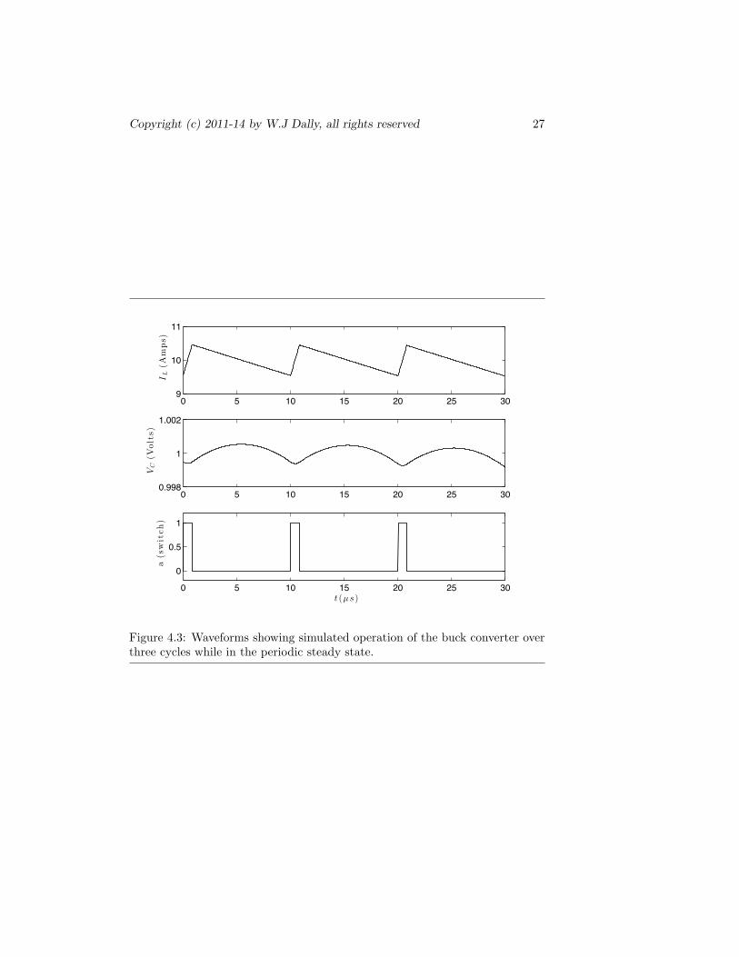
Copyright (c) 2011-14 by W.J Dally, all rights reserved 27
0 5 10 15 20 25 309
10
11
IL(A
mps)
0 5 10 15 20 25 300.998
1
1.002
VC(V
olts)
0 5 10 15 20 25 30
0
0.5
1
a(switch)
t (µ s)
Figure 4.3: Waveforms showing simulated operation of the buck converter overthree cycles while in the periodic steady state.

28 Green Electronics
0 100 200 300 400 500 600 700 800 900 1000−10
−5
0
5
10
IL(A
mps)
0 100 200 300 400 500 600 700 800 900 1000−0.5
0
0.5
1
1.5
2
2.5
VC(V
olts)
t (µ s)
Figure 4.4: Waveforms showing simulated operation of the buck converter over1ms during a turn-on transient with zero load current. The output voltageovershoots by a factor of two and oscillates with a period of 628 µs.
The second trace shows a very small ripple on vC . Which varies by ±0.5mVabout the target voltage of vref = 1V. Again the actual curve is part of a sinewave - since its generated by a tank circuit. However, it is closely approxi-mated by a parabola because it is the integral of the current which is closelyapproximated by a line.
The bottom trace of the figure shows the position of the switch. The dutyfactor is set to 1/12 to give the steady state condition for the 12:1 step downratio of our example converter.
Figure 4.4 shows a simulation of the buck converter for 1ms of simulated time.The simulation shows a startup transient with initial conditions of il0 = vc0 = 0.This simulation uses our high-frequency model to simulate the low-frequencybehavior of the converter.
As expected from Equation (3.14), without a controller the converter os-cillates in response to the transient with frequency ω = (LC)−1/2 and henceperiod T = 2π
√LC. In this case T = 628µs.
If an actual converter oscillated in this manner it would most likely destroythe downstream circuit. A circuit designed for a 1V supply typically cannotwithstand a 100% overshoot to 2V.

Copyright (c) 2011-14 by W.J Dally, all rights reserved 29
% simulate one time step - low frequency modeldi_l = (d*v_s-v_c)*dt/l ;dv_c = (i_l - i_load)*dt/c ;i_l = i_l + di_l ;v_c = v_c + dv_c ;
Figure 4.5: Matlab simulation model to advance the state of the buck converterby one timestep, dt, using a low-frequency approximation.
4.2 Low-Frequency Model
Figure 4.4 shows that we can use our high-frequency model to simulate the low-frequency behavior of the converter. However, it is inefficient to do so. We canreduce our simulation time by an order of magnitude or more by using a modelthat directly reflects the low-frequency behvavior of the converter as capturedin Equations (3.9) and (3.10) directly.
Figure 4.5 shows a low-frequency simulation model for the buck converter.The first line computes the change in inductor current averaged over the cycle.We are not concerned with the position of the switch, but rather abstract theswitching into the duty factor variable d. Otherwise the model is identical tothat of Figure 4.1. With this small change, however, we can get by with a muchlarger step size dt resulting in fewer steps per switching cycle and a much fastersimulation.
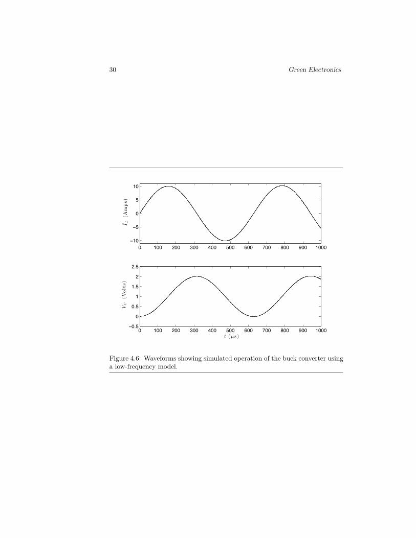
Figure 4.6 shows waveforms generated using the Matlab model of Figure 4.5with initial conditions of vC = iL = 0 and 20 steps per switching cycle (dt=0.5µs. The step size here must be kept small enough to avoid excessive errors inour rectangular integration formula. Using a better integration formula wouldenable a smaller step size.
Except for the missing ripple, which is not modeled by the low-frequencymodel, the response is identical to that produced by our high-frequency model.
4.3 Exercises
simulate buck with different initial conditionsbetter integration formula
30 Green Electronics
0 100 200 300 400 500 600 700 800 900 1000−10
−5
0
5
10
IL
(Amps)
0 100 200 300 400 500 600 700 800 900 1000−0.5
0
0.5
1
1.5
2
2.5
VC
(Volts)
t (µ s)
Figure 4.6: Waveforms showing simulated operation of the buck converter usinga low-frequency model.
Chapter 5
Controlling the BuckConverter
In Chapters 3 and 4 we saw through both analysis and simulation that the buckconverter, by itself, is unstable. A transient in either duty factor or load leadsto an undamped oscillation in both output voltage vC and inductor current iL.In many cases such oscillations would destroy the load.
A good controller modifies the dynamics of the system to make it stable,avoid overshoot, and give fast response to transients. There are many strategiesfor controlling a buck converter which we will visit in future chapters. In thischapter we illustrate the principles of control using a simple PD (proportional-derivative) feedback controller.
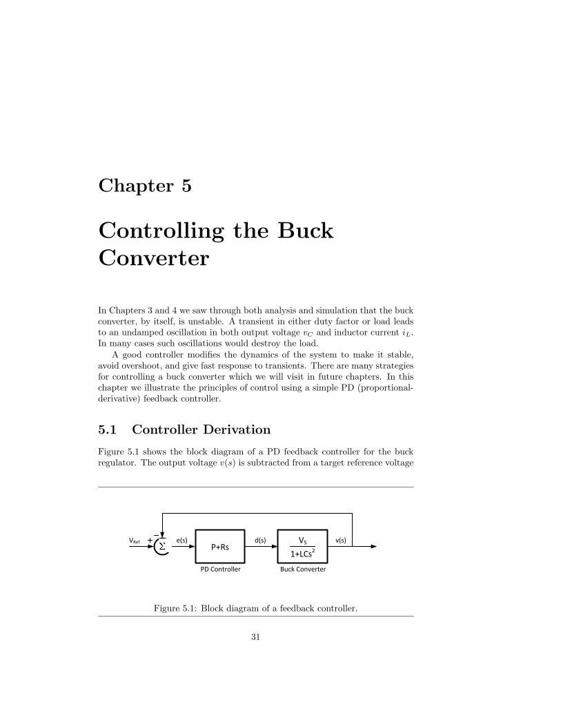
5.1 Controller Derivation
Figure 5.1 shows the block diagram of a PD feedback controller for the buckregulator. The output voltage v(s) is subtracted from a target reference voltage
VS
1+LCs2
Buck Converter
P+Rs
PD Controller
d(s) v(s)e(s)VRef
Figure 5.1: Block diagram of a feedback controller.
31

32 Green Electronics
VRef(s) to generate an error signal e(s). A PD controller applies a proportionalgain P and a derivative gain Rs to the error signal to generate a control signald(s) = (P + Rs)e(s). Here the duty factor is the control input to the buckconverter.
The open-loop transfer function of this system is
H(s) =v(s)e(s)
=VS(P +Rs)1 + LCs2
=(KP +KRs)s2 + 1
LC
(5.1)
Where K = VS/LC. Closing the feedback loop gives a closed-loop transferfunction of
G(s) =v(s)
VRef(s)
=H(s)
1 +H(s)
=(KP+KRs)
s2+ 1LC
1 + (KP+KRs)
s2+ 1LC
=KP +KRs
s2 +KRs+KP + 1LC
(5.2)
The denominator of equation (5.2) determines the frequency ω and dampingfactor ζ of our closed-loop system. Its natural frequency is the square root ofthe constant term
ω =
√KP +
1LC
(5.3)
Its damping factor is given by the linear term
ζ =KR
2ω(5.4)
We can rewrite (5.3) to give an expression for P
P =ω2 − 1
LC
K=LCω2 − 1KLC
(5.5)
and we can rearrange (5.4) to give an expression for R:

Copyright (c) 2011-14 by W.J Dally, all rights reserved 33
v(t)
VRef
e
dedt
RP
e+ RP
dedt
ti ti+RP
Figure 5.2: PD control is equivalent to looking ahead and providing proportionalfeedback at the value projected R
P in the future.
R =2ζωK
(5.6)
If we choose ω = 2.2 × 10⁴ and ζ = 1 (critically damped) we get P = 1/3and R = 3.7 × 10⁻⁵. We need to choose ω to keep f = ω/2π well below (atleast a factor of 10 below) the switching frequency to preserve our continuoustime approximation. It should also be chosen to minimize non-linear behaviorby avoiding saturating the control variable. Too high a gain will lead to dutyfactors being commanded outside the legal range.
The intuition behind proportional feedback, the P term, is simple. If we havean error in a certain direction, we apply an input proportional to the error. Ifour output voltage is below the reference voltage we apply a positive input todrive it higher. The larger the error, the larger the input.
Unfortunately, proportional feedback is not sufficient to control a second-order system like the buck converter. The inductor current gives the systemmomentum. Once the output voltage is rising, the inductor current will causeit to continue to rise - even if we set the duty factor to zero. To control sucha system we need to compute a control input based not only on the error butalso on the derivative of the error.
Derivative feedback has the effect of compensating for the momentum in thesystem by looking ahead and providing feedback based on the projected futurevalue of the system output. This is illustrated in Figure 5.2. The figure showsa system where e(t) has a positive value e and a negative slope de/dt at time ti.A PD controller effectively looks ahead to time ti + R/P assuming a constant

34 Green Electronics
% control law - runs once per cycleer = v_ref - v_c ;der = (er - old_er)/t_c ;old_er = er ;d = er*P + der*R + d0;d = max(0,min(d_max,d)) ;
Figure 5.3: Matlab code for PD controller for buck converter.
slope and applies a control input based on that predicted value. By settingthe derivative gain appropriately the look ahead interval can be set to criticallydamp the response - so that the error smoothly goes to zero without overshoot.
We will disuss control methods in more detail in future sections.
5.2 Controller Simulation
We can verify our controller, and the validity of the assumptions on which it isbased, through simulation. Figure 5.3 shows Matlab code implementing our PDcontroller. This code runs once each switching cycle. It computes the error er,approximates the derivative of the error using forward differencing to calculateder. It then applies the control law to compute the duty factor d.
We add the duty factor needed to maintain the correct steady state outputvoltage d0 = 1/12 to the control law to give the correct output voltage whenthe error is zero. Finally, we limit the pulse width to its legal range. Thislimit is important because many PWM generators will wrap out of limit values.This can result in a small negative value of d resulting in a large pulse width— leading to catastrophic effects. The limit causes our controller to saturaterather than wrap when the control variable goes out of range.
In an optimized controller we would avoid the divide by folding 1/tc into theconstant multiplied by der. With this optimization the control law is four adds,two multiplies (by constants), and a limit operation. Even a slow microcontrollercan perform the 7 operations needed to implement this loop fast enough to keepup with a 100kHz converter.
Figure 5.4 shows the response of the buck converter with PD controller tothe startup transient. The conditions are identical to those shown in Figure 4.4except for the addition of the controller. We see that the addition of feedbackcontrol, with appropriately selected parameters P and R, eliminates the oscil-latory behavior. The output voltage vC (middle panel) quicly converges to thetarget value with no overshoot.
The bottom panel shows the pulse width ta and illustrates the non-linearnature of this controller. After four cycles, the inductor current is pumped up toabout 9A and the slope of vc becomes so steep that the PD control law computesa negative duty factor. The last line of Figure 5.3 clamps this value to zero. The

Copyright (c) 2011-14 by W.J Dally, all rights reserved 35
0 50 100 150 200 250 300 350 400 450 500
0
5
10
i L(A
mps)
0 50 100 150 200 250 300 350 400 450 500
0
0.5
1
vC(V
olts)
0 50 100 150 200 250 300 350 400 450 5000
2
4
t a(µ
s)
t (µ s)
Figure 5.4: Response of the buck converter with a PD controller to the start uptransient.

36 Green Electronics
0 100 200 300 400 500 600 700−202468
i L(A
mps)
0 100 200 300 400 500 600 7000.8
1
vC(V
olts)
0 100 200 300 400 500 600 7000
2
4
t a(µ
s)
t (µ s)
Figure 5.5: Response of the buck converter with a PD controller to a 5A currentstep at 100µs and a -3A current step at 400µs.
pulse width remains at zero for 11 cycles. Fortunately this non-linear behaviordoes not result in any overshoot. This is not always the case. Linear controltheory does not completely predict the behavior of control systems where thecontrol variables saturate.
Figure 5.5 shows the response of the controller to load current transients.Load currently steps from 0 to 5A at 100µs and then down to 2A at 400 µs.In each case the transient causes an initial disturbance in vc. The controllerthen acts to drive the system back to vc = 1 with no overshoot. The controllergoes sligtly non-linear on the negative transient when a negative duty factor iscomputed and clamped to zero.
5.3 Exercises
Compute P and R for various values of L, C, V SWhat if V S changes?What is upper limit on PAdd integral control term - deal with windup
Chapter 6
Boost and Buck-BoostConverters
Now that we understand the operation and control of the buck converter, we willexplore its two close relatives: the boost converter, and the buck-boost converter.All three of these converters, the buck, boost, and buck-boost, are called non-isolated converters because their input and output share one terminal. We willvisit isolated converters, where the input and output share no terminals and canfloat with respect to one another in Chapter 10.
These three types of converters are used to provide output voltages in differ-ent ranges. A buck converter is used to convert an input voltage VS to a lowervoltage vC ≤ VS of the same polarity. A boost converter, which is just a buckconverter connected backwards, does the opposite. It boosts an input voltageVS to a higher output voltage vC ≥ VS of the same polarity. A buck-boostconverter is used to convert an input voltage VS to an output voltage vC ofopposite polarity.
All three of the basic non-isolated converters (buck, boost, and buck-boost)use the same basic cell consisting of an inductor with one end connected to a twoposition switch. All three converters also have three terminals: input, output,and ground. The type of converter is determined by how the cell is connectedto the terminals, specifically by which terminal is connected to the free end ofthe inductor. There are three possibilities: When the free end of the inductoris connected to the output we have a buck converter. When the free end of theinductor is connected to the input we have a boost converter (a buck connectedbackwards). Finally, when the free end of the inductor is connected to groundwe have a buck-boost converter.
6.1 Boost Converter
Figure 6.1 shows a boost converter which is used to boost input voltage VS to ahigher output voltage vC ≥ VS . A boost converter is just a buck converter with
37

38 Green Electronics
VS
+
-
vC Load
+
C
L
iL
a
b
iLoad
Figure 6.1: A boost converter. Input voltage VS is boosted to output voltagevc ≥ VS . A boost converter is simply a buck converter connected backwards —i.e., with input and output swapped.
its input and output swapped. Comparing Figure 6.1 with Figure 2.3 sourceVS is swapped with the capacitor C (and the load) and the polarity of inductorcurrent iL is reversed. If a buck or boost is realized using switches that cancarry current in either direction then power can flow in either direction and thetwo circuits are identical.
Boost converters are widely used any time an output voltage higher thanthe input voltage is required. They are used, for example, in power-factorcorrection input stages (Chapter 16) where they boost the rectified AC inputvoltage, which varies from 0V to 170V, to a higher intermediate DC voltage,often 200-400V, while keeping the input current proportional to the AC inputvoltage.
Figure 6.2 illustrates operation of the boost converter over two switchingcycles in a periodic steady state. By convention we consider the cycle to startwith the switch down, in position b. During the time tb that the switch is down,the right end of the inductor is tied to ground, input voltage VS is applied acrossthe inductor, and the inductor current ramps with slope diL
dt = VS
L . Startingfrom an initial value of i0, at time tb the current has reached
ip = i0 +tbVS
L. (6.1)
During the second half of the cycle the switch is up, in position a, and theright side of the inductor is connected to vC . The voltage across the inductor isVS − vC , which has a negative value in the periodic steady state since vC > VS .During this part of the cycle, the inductor current decreases with slope diL
dt =VS−vC
L .For the converter to be in the periodic steady state we must have the volt-
seconds across the inductor sum to zero over the cycle:
tbVS + ta (VS − vC) = 0. (6.2)

Copyright (c) 2011-14 by W.J Dally, all rights reserved 39
ip
i0
t0 tb tcy
iL
b/a
tb ta
Figure 6.2: Waveforms showing operation of the boost converter.
If we denote the duty factor of the switch in position a as D = ta
ta+tb= ta
tcy, we
can rewrite this as:
(1−D)VS +D (VS − vC) = 0.VS −DvC = 0
DvC = VS
vC =VS
D. (6.3)
Which is just a rederivation of (2.8) with vC and VS reversed, VS = DvC .Many books describe the boost converter in terms of the duty factor of the
switch in position b. If we define Db = tb
tcy= 1−D we can rewrite (6.3) as
vC =VS
1−Db. (6.4)
Which is the more common form of (6.3) but one which makes it harder to seethe relationship to the buck converter.
6.2 Buck-Boost Converter
Figure 6.3 shows a buck-boost converter which is used to produce a negativeoutput voltage vC from a positive input voltage VS . When the switch is in
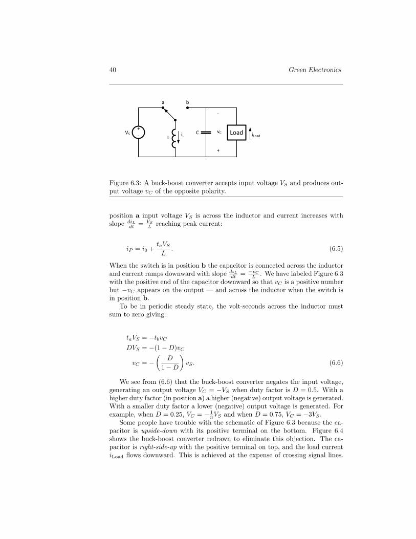
40 Green Electronics
VS
+
- vC Load
+
C
a b
iLoadLiL
Figure 6.3: A buck-boost converter accepts input voltage VS and produces out-put voltage vC of the opposite polarity.
position a input voltage VS is across the inductor and current increases withslope diL
dt = VS
L reaching peak current:
iP = i0 +taVS
L. (6.5)
When the switch is in position b the capacitor is connected across the inductorand current ramps downward with slope diL
dt = −vC
L . We have labeled Figure 6.3with the positive end of the capacitor downward so that vC is a positive numberbut −vC appears on the output — and across the inductor when the switch isin position b.
To be in periodic steady state, the volt-seconds across the inductor mustsum to zero giving:
taVS = −tbvC
DVS = −(1−D)vC
vC = −(
D
1−D
)vS . (6.6)
We see from (6.6) that the buck-boost converter negates the input voltage,generating an output voltage VC = −VS when duty factor is D = 0.5. With ahigher duty factor (in position a) a higher (negative) output voltage is generated.With a smaller duty factor a lower (negative) output voltage is generated. Forexample, when D = 0.25, VC = − 1
3VS and when D = 0.75, VC = −3VS .Some people have trouble with the schematic of Figure 6.3 because the ca-
pacitor is upside-down with its positive terminal on the bottom. Figure 6.4shows the buck-boost converter redrawn to eliminate this objection. The ca-pacitor is right-side-up with the positive terminal on top, and the load currentiLoad flows downward. This is achieved at the expense of crossing signal lines.

Copyright (c) 2011-14 by W.J Dally, all rights reserved 41
VS
+
-
vC Load
+
C
a b
iLoad
LiL
Figure 6.4: The buck-boost converter of Figure 6.3 redrawn so that the outputcapacitor has its positive terminal on top.
The circuit of Figure 6.4 is identical to that of Figure 6.3 however, some peoplefind this version easier to understand.
6.3 Exercises
Cuk

42 Green Electronics
Chapter 7
Analysis and Control of theBoost Converter
The boost converter, while it is just a buck converter connected backwards, hassignificantly different dynamics than the buck converter. A decrease inDa of theboost gives a small immediate decrease and a long-term increase in the outputvoltage VC . This short term decrease in VC manifests itself as a right-half-planezero in the transfer functino of the boost which makes the boost significantlyharder to control than the buck — which lacks this zero.
In this chapter we develop a dynamic model of the boost converter. Wesee that this model is non-linear and hence does not admit the easy controlsolution we applied to the buck. We use this non-linearity as an opportunity tointroduce layered control and develop a layered controller for the boost converter.In Chapter 8 we solve the same problem in a different manner by building alinearized small signal model of the boost converter and designing a conventionalPD controller based on this model.
7.1 Analysis of the Boost Converter
When the boost converter is not in periodic steady state the change in inductorcurrent over one cycle is given by dividing the volt-seconds imbalance by L:
∆ii =tcy ((1−D)VS +D (VS − vi))
L
∆ii =tcy (VS −Dvi)
L(7.1)
The change in capacitor voltage over one cycle is given by the current imbalance:
43

44 Green Electronics
∆vi =tcy
(Dii − iLoad
)C
. (7.2)
The inductor only supplies current to the output capacitor when the switch isin position a. Thus i is muliplied by D in (7.2) to give the average inductorcurrent seen by the output capacitor.
If we convert difference equations (7.1) and (7.2) to differential equationsand take their Laplace transforms we get
i(s) =VS −D(s)v(s)
Ls(7.3)
v(s) =D(s)i(s)− iLoad(s)
Cs(7.4)
Combining gives
i(s) =VS
Ls− D2(s)i(s)−D(s)iLoad(s)
LCs2
LCi(s)s2 = CVss−D2(s)i(s) +D(s)iLoad(s)
LCi(s)s2 +D2(s)i(s) = CVss+D(s)iLoad(s)
i(s) =CVss+D(s)iLoad(s)
LCs2 +D2(s)(7.5)
Substituting into (7.4) gives
v(s) =CVsD(s)s+D2(s)iLoad(s)
LCs2+D2(s)
Cs
v(s) =CVsD(s)s2 +D2(s)iLoad(s)s
LC2s2 + CD2(s)(7.6)
Ignoring the contribution from ILoad this simplifies to
v(s) =VsD(s)s2
LCs2 +D2(s)(7.7)
From (7.7) we see that even though a boost is just a buck connected back-wards it has significantly different dynamics. We cannot easily write a transferfunction v(s)/d(s) for the boost. The response from d to v is non-linear - thereis a d2 term in the (7.7). Also, the response from d to v acts in both directionsas indicated by d appearing in both the numerator and denominator of (7.7).In the short term increasing d increases v because the increased duty factorprovides a larger fraction of the inductor current to the capacitor. However,over time a larger d decreases i and hence decreases v.
Copyright (c) 2011-14 by W.J Dally, all rights reserved 45
D
Cs
Voltage Stage
VS-DvC
Ls
ieitV
Cont
Dve i
Current Stage
vVref I
Cont
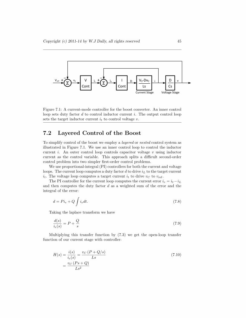
Figure 7.1: A current-mode controller for the boost converter. An inner controlloop sets duty factor d to control inductor current i. The output control loopsets the target inductor current it to control voltage v.
7.2 Layered Control of the Boost
To simplify control of the boost we employ a layered or nested control system asillustrated in Figure 7.1. We use an inner control loop to control the inductorcurrent i. An outer control loop controls capacitor voltage v using inductorcurrent as the control variable. This approach splits a difficult second-ordercontrol problem into two simpler first-order control problems.
We use proportional-integral (PI) controllers for both the current and voltageloops. The current loop computes a duty factor d to drive iL to the target currentit. The voltage loop computes a target current it to drive vC to vref .
The PI controller for the current loop computes the current error ie = it−iLand then computes the duty factor d as a weighted sum of the error and theintegral of the error:
d = Pie +Q
∫iedt. (7.8)
Taking the laplace transform we have
d(s)ie(s)
= P +Q
s(7.9)
Multiplying this transfer function by (7.3) we get the open-loop transferfunction of our current stage with controller:
H(s) =i(s)ie(s)
=vC (P +Q/s)
Ls(7.10)
=vC (Ps+Q)
Ls2

46 Green Electronics
Closing the loop gives:
G(s) =vC (Ps+Q)
Ls2 + vCPs+ vCQ(7.11)
=vCP
L s+ vCQL
s2 + vCPL s+ vCQ
L
From the denominator of (7.12) we calculate:
ω =
√vCQ
L(7.12)
ζ =vCP
2Lω(7.13)
Q =ω2L
vC(7.14)
P =2LζωvC
(7.15)
For the current loop we choose ω = 6.28 × 10⁴ (f=10kHz) and ζ = 1. Forour example converter with vC = 250V and L = 500µH we derive P = 0.251and Q = 7.88× 10³.
For the voltage loop, combining the PI controller with (7.4), ignoring theload current, and considering D to be a constant we get the open-loop transferfunction:
v(s)ve(s)
=D(P + Q
s
)Cs
=D(Ps+Q)
Cs2(7.16)
This gives a closed-loop transfer function of
H(s) =DPC s+ DQ
C
ss + DPC s+ DQ
C
(7.17)
So we have
ω =√DQ/C (7.18)
ζ =DP
2Cω(7.19)
Q =ω2C
D(7.20)
P =2CζωD
(7.21)

Copyright (c) 2011-14 by W.J Dally, all rights reserved 47
% control law - execute once per t_c% PI voltage controllerer = v_ref - v_c ;ier = ier + er*t_c ;i_t = er*P + ier*Q ;
% current controllerer2 = i_t - i_l ;ier2 = ier2 + er2*t_c ;d2 = er2*P2+ier2*Q2+D ;t_a = d2*t_c ;t_a = max(0,min(t_amax,t_a)) ;
Figure 7.2: Matlab code implementing the layered controller given by (??) and(??).
Note that the parameters in (??) are different than the parameters with thesame symbols in (7.15). We choose not to subscript them to avoid clutteringthe equations.
For stability we must operate the voltage control loop with a lower naturalfrequency than the current control loop, so that transients to the current loophave settled out before the voltage loop advances. We choose ω = 5 × 10³
(f = 800Hz). With ζ = 1 and C = 10µF we have P = 0.25 and Q = 7.88× 10³.
7.3 Simulation
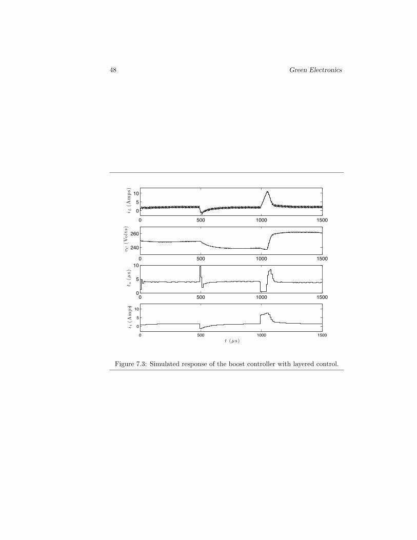
To validate our layered controller, we simulate it using Matlab. Matlab codefor our controller is shown in Figure 7.2. Figure 7.3 shows the response of thesystem to two steps on Vref . Vref starts at 250 V and is set to 240 V at 500µsand to 260V at 1ms.
The waveform for the target current in the bottom panel of Figure 7.3 showsthe effect of controller non-linearity. At 1ms the voltage controller commands asteep increase in it. In an attempt to comply the current loop runs out of rangeon ta (third panel of Figure 7.3). The waveform for iL tracks that of it veryclosely except in cases like this where the control actuator saturates. In somecases control saturation can result in undesired overshoot as the response of thenon-linear system deviates from the linear response. In such cases the controlparameters should be adjusted to avoid saturation.
7.4 Exercises
controller with voltage loop at 1kHz - saturates variables and overshootsapply current mode control to a buck
48 Green Electronics
0 500 1000 1500
0510
i L(A
mps)
0 500 1000 1500
240
260
vC(V
olts)
0 500 1000 15000
5
10
t a(µ
s)
0 500 1000 1500
0
5
10
i t(A
mps)
t (µ s)
Figure 7.3: Simulated response of the boost controller with layered control.

Copyright (c) 2011-14 by W.J Dally, all rights reserved 49
apply current mode control to a buck-boostadd ESR to capacitorderive equation with load resistancedraw bode plots

50 Green Electronics

Chapter 8
Small-Signal Analysis of theBoost Converter
In Chapter 7 we derived the dynamics of the boost converter. Because theconverter was non-linear, we could not apply the direct approach to controlthat we used on the buck converter in Chapter 5. Instead we used a layeredcontroller consisting of two PI control loops: an inner loop controlling inductorcurrent and an outer loop controlling voltage.
In this chapter we take a different approach to controlling the boost regu-lator. We develop a linear transfer function for the boost converter by makinga small-signal approximation. For small deviations about its steady-state oper-ating point the boost converter will behave nearly linearly. We derive its lineartransfer function for small perturbations about the operating point and in turnderive a control law based on this transfer function. We need to understand,however, that the resulting control law will only be valid in a small region aroundthe original operating point.
8.1 Impulse Response
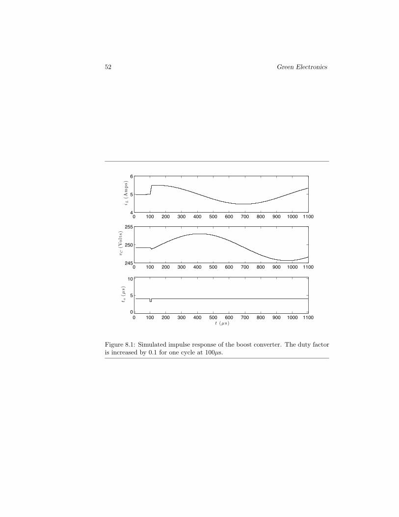
We can visualize the linearized transfer function of the boost converter by sim-ulating its impulse response. Suppose the converter is operating in the steadystate with current iL = I, voltage vC = V , and duty factor d = D. From thisstate we purturb it by applying a duty factor of d = D + d for one cycle. Theresulting response is the scaled impulse response of the converter.
Figure 8.1 shows the simulated impulse response of our example boost con-verter. The converter is operating in periodic steady state until t=100µs whenthe duty factor is decreased by 0.1 for one cycle (i.e., d = −0.1). The result is awaveform on vC that first dips slightly and then oscillates with a 1.1ms periodand an amplitude of 3.6V.
51
52 Green Electronics
0 100 200 300 400 500 600 700 800 900 1000 11004
5
6
i L(A
mps)
0 100 200 300 400 500 600 700 800 900 1000 1100245
250
255
vC(V
olts)
0 100 200 300 400 500 600 700 800 900 1000 11000
5
10
t a(µ
s)
t (µ s)
Figure 8.1: Simulated impulse response of the boost converter. The duty factoris increased by 0.1 for one cycle at 100µs.

Copyright (c) 2011-14 by W.J Dally, all rights reserved 53
8.2 Small-Signal Model
To derive a small signal model of the boost converter we start with the differenceequations (7.1) and (7.2) and perturb them. For each of the variables d, i,and v we replace the variable by its steady state component (D, I, and V )plus its small-signal component (d,i, and v). We then make the small-signalapproximation by discarding the cross terms, e.g., id, since the product of twosmall things is too small to consider. We also discard strictly steady-state terms.
Applying the small-signal approximation to (7.1) and (7.2) gives
∆itcy
= − 1L
(dV +Dv
)(8.1)
∆vtcy
=1C
(dI +Di
)(8.2)
Approximating the left hand sides as derivatives and taking Laplace transformsgives
i(s) = − 1Ls
(V d(s) +Dv(s)
)(8.3)
v(s) =1Cs
(Id(s) +Di(s)
)(8.4)
Substituting (8.3) into (8.4) gives
v(s) =(I
Cs− DV
LCs2
)d(s)− D2
LCs2v(s)
v(s)(
1 +− D2
LCs2
)=(I
Cs− DV
LCs2
)d(s)
v(s) =
(I
Cs −DV
LCs2
)d(s)
1 + D2
LCs2
v(s)
d(s)=
ILs−DV
LCs2 +D2(8.5)
We can write (8.5) in a form that makes the parameters of the transfer functionmore explicit as:
v(s)
d(s)= Kb
sω1− 1
s2
ω20
+ 1(8.6)
where
54 Green Electronics
−50
0
50
100
Mag
nitu
de (d
B)
103 104 105 10690
135
180
225
270
315
360
Phas
e (d
eg)
Bode Diagram
Frequency (rad/s)
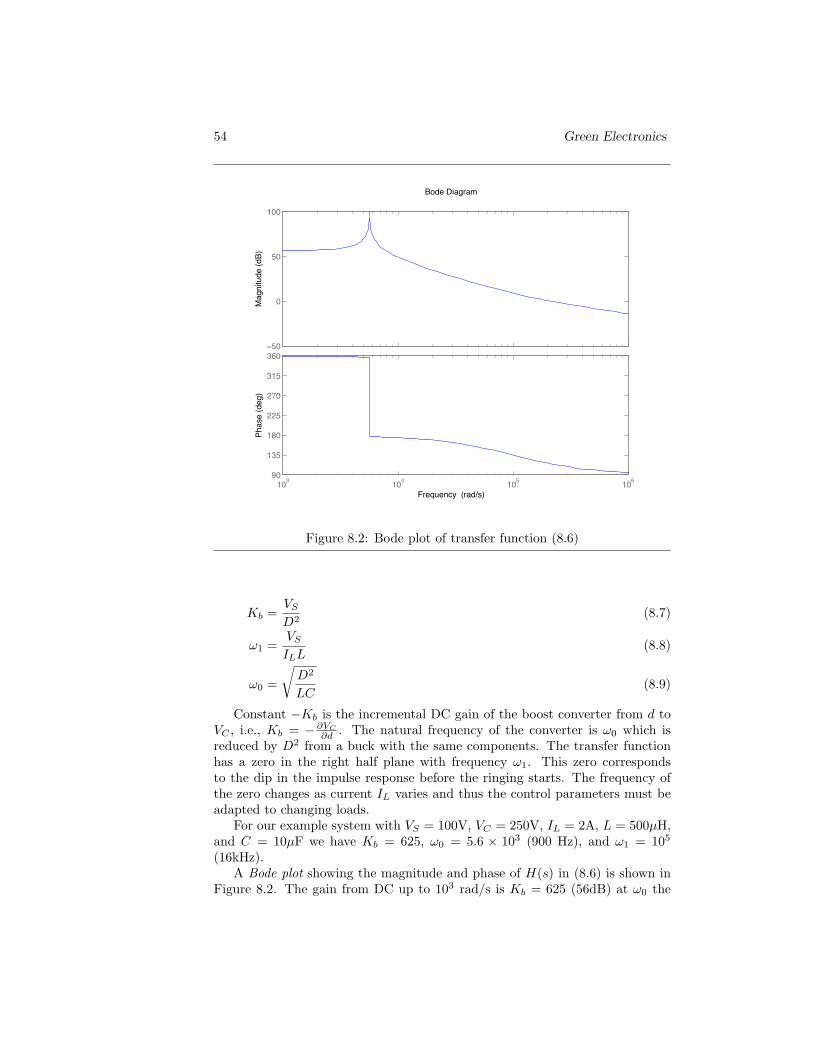
Figure 8.2: Bode plot of transfer function (8.6)
Kb =VS
D2(8.7)
ω1 =VS
ILL(8.8)
ω0 =
√D2
LC(8.9)
Constant −Kb is the incremental DC gain of the boost converter from d toVC , i.e., Kb = −∂VC
∂d . The natural frequency of the converter is ω0 which isreduced by D2 from a buck with the same components. The transfer functionhas a zero in the right half plane with frequency ω1. This zero correspondsto the dip in the impulse response before the ringing starts. The frequency ofthe zero changes as current IL varies and thus the control parameters must beadapted to changing loads.
For our example system with VS = 100V, VC = 250V, IL = 2A, L = 500µH,and C = 10µF we have Kb = 625, ω0 = 5.6 × 10³ (900 Hz), and ω1 = 105
(16kHz).A Bode plot showing the magnitude and phase of H(s) in (8.6) is shown in
Figure 8.2. The gain from DC up to 103 rad/s is Kb = 625 (56dB) at ω0 the

Copyright (c) 2011-14 by W.J Dally, all rights reserved 55
phase abruptly shifts to 180 degrees and the magnitude starts rolling off at 20dBper decade. At 3 × 10⁴ rad/s the phase starts shifting by another 90 degreesdue to the zero at ω1 = 105 rad/s. The unity-gain frequency is 2.2× 10⁵ rad/s.
8.3 Controller Design
To stabilize the system we will use a PD controller P + Rs to accomplish twomodifications to the Bode plot of Figure 8.2. First, we use a small proportionalgain P < 1 to reduce the DC gain. This reduces the unity-gain frequency of thesystem — moving it well below the zero at 105 rad/s. Second, we add a zeroat ωc = P/R to advance the phase at the new unity gain point well above 180degrees.
For stability we would like a phase margin of at least 60 at the unity gainfrequency. To achieve this we choose P = 5 × 10⁻³ to reduce the unity-gainfrequency, and ωc = 6×10³ rad/s to add phase margin. This gives R = P/ωc =8.3× 10⁻⁷.
Adding a PD controller to (8.6) gives an open-loop transfer function of
H(s) = Kb
(P +Rs)(
sω1− 1)
s2
ω20
+ 1
=
(KbRω1
)s2 +
(KbPω1
−Kb
)s−KbP
s2
ω20
+ 1(8.10)
A Bode plot of this transfer function with our choice of P and R is shown inFigure 8.3. We have reduced the unity-gain frequency to 2×10⁴ rad/s and havea 62 phase margin.
Figure 8.4 shows simulated waveforms from the boost regulator with thisPD controller. The figures shows the response to a step in Vref from 250V to240V at 400µs and from 240V to 260V at 800µs. In both cases the convertertakes about 200µs (20 PWM cycles) to respond without overshoot.
8.4 Exercises

56 Green Electronics
−20
−10
0
10
20
30
40
50
Mag
nitu
de (d
B)
103 104 105 106180
225
270
315
360
405
450
Phas
e (d
eg)
Bode DiagramGm = 15.6 dB (at Inf rad/s) , Pm = 61.8 deg (at 1.94e+04 rad/s)
Frequency (rad/s)
Figure 8.3: Bode plot of transfer function (8.10)

Copyright (c) 2011-14 by W.J Dally, all rights reserved 57
0 200 400 600 800 1000 1200
0
2
4
6
i L(A
mps)
0 200 400 600 800 1000 1200240
250
260
vC(V
olts)
0 200 400 600 800 1000 12000
5
10
t a(µ
s)
t (µ s)
Figure 8.4: Simulated response of boost converter with PD controller.

58 Green Electronics

Chapter 9
Analysis and Control of theBuck-Boost Converter
9.1 Analysis of the Buck-Boost Converter
The change in inductor current over one cycle for the buck-boost converter ofFigure 6.3 is given by
∆ii =(taVS − tbvi)
L
∆ii =tcy (DVS − (1−D)vi)
L(9.1)
Where D is the duty factor of the switch in position a. Much like the boostconverter, the change in capacitor voltage over one cycle is given by
∆vi =tcy
(Dbii − iLoad
)C
∆vi =tcy
((1−D)ii − iLoad
)C
(9.2)
Converting to Laplace transforms gives
i(s) =VSD(s)− (1−D(s))vi(s)
Ls(9.3)
v(s) =(1−D(s))i(s)− iLoad(s)
Cs(9.4)
59

60 Green Electronics
Chapter 10
Isolated Converters
The buck, boost, and buck-boost converters discussed in previous chapters arethe widely used in applications when the input and output can share a supplyterminal and where the step-up or step-down ratio is small. Whenever either ofthese conditions is not true, an isolated converter is required. Isolated convert-ers, as the name imply isolate the input and output ports so that they may floatrelative to one another. In some cases the absolute input and output voltagesmay differ by thousands of volts. Most isolated converters use a transformer attheir core to provide isolation.
Transformer-based converters are also used when the step-up or step-downratio is large — particulary when large amounts of power are being converted.The use of a transformer in these cases enables a more economical and efficientconverter. The switch of a buck converter must handle both the high inputvoltage of the converter and its high output current. With a transformer wecan design a converter where a switch that handles the high input voltage onlysees the low input current and a switch that handles the high output currentonly sees the low output voltage. For a converter with a N : 1 step-down ratiothis can reduce the cost of the switches by a factor of N2.
In this chapter we start our discussion of isolated converters by introducingthe ideal transformer. We go on to discuss the limitiations of real transformers— that include magnetizing and leakage inductance. Finally we show a full-bridge converter that employs a transformer in an isolated analog of the buckconverter.
10.1 The Ideal Transformer
Most isolated converters use transformers. A schematic symbol for a transformerwith two windings1 is shown in Figure 10.1. The symbol is two back-to-back coilsor windings. While the same winding symbol is used for an inductor, there is no
1While a transformer may have any number of windings we will most commonly deal withtwo-winding transformers.
61
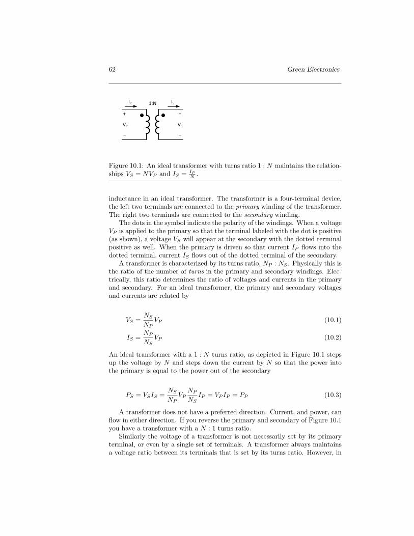
62 Green Electronics
1:NIP
VP
IS
VS
+ +
Figure 10.1: An ideal transformer with turns ratio 1 : N maintains the relation-ships VS = NVP and IS = IP
N .
inductance in an ideal transformer. The transformer is a four-terminal device,the left two terminals are connected to the primary winding of the transformer.The right two terminals are connected to the secondary winding.
The dots in the symbol indicate the polarity of the windings. When a voltageVP is applied to the primary so that the terminal labeled with the dot is positive(as shown), a voltage VS will appear at the secondary with the dotted terminalpositive as well. When the primary is driven so that current IP flows into thedotted terminal, current IS flows out of the dotted terminal of the secondary.
A transformer is characterized by its turns ratio, NP : NS . Physically this isthe ratio of the number of turns in the primary and secondary windings. Elec-trically, this ratio determines the ratio of voltages and currents in the primaryand secondary. For an ideal transformer, the primary and secondary voltagesand currents are related by
VS =NS
NPVP (10.1)
IS =NP
NSVP (10.2)
An ideal transformer with a 1 : N turns ratio, as depicted in Figure 10.1 stepsup the voltage by N and steps down the current by N so that the power intothe primary is equal to the power out of the secondary
PS = VSIS =NS
NPVP
NP
NSIP = VP IP = PP (10.3)
A transformer does not have a preferred direction. Current, and power, canflow in either direction. If you reverse the primary and secondary of Figure 10.1you have a transformer with a N : 1 turns ratio.
Similarly the voltage of a transformer is not necessarily set by its primaryterminal, or even by a single set of terminals. A transformer always maintainsa voltage ratio between its terminals that is set by its turns ratio. However, in
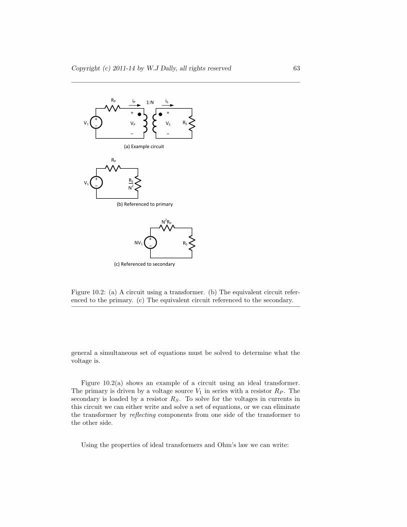
Copyright (c) 2011-14 by W.J Dally, all rights reserved 63
1:NiP
VP
iS
VS
+ +
V1
+
RP
RS
V1
+
RP
RS
(a) Example circuit
N2
(b) Referenced to primary
NV1
+
N2RP
RS
(c) Referenced to secondary
Figure 10.2: (a) A circuit using a transformer. (b) The equivalent circuit refer-enced to the primary. (c) The equivalent circuit referenced to the secondary.
general a simultaneous set of equations must be solved to determine what thevoltage is.
Figure 10.2(a) shows an example of a circuit using an ideal transformer.The primary is driven by a voltage source V1 in series with a resistor RP . Thesecondary is loaded by a resistor RS . To solve for the voltages in currents inthis circuit we can either write and solve a set of equations, or we can eliminatethe transformer by reflecting components from one side of the transformer tothe other side.
Using the properties of ideal transformers and Ohm’s law we can write:

64 Green Electronics
IP =V1 − VP
RP(10.4)
VP =1NVS (10.5)
IP = NIS (10.6)
IS =VS
RS(10.7)
We can solve these four equations in four unknowns for VP , VS , IP , and IS .An alternate approach is to reflect the secondary resistor RS to the primary
as shown in Figure 10.2(b). If we reflect an impedance Z from winding A of atransformer to winding B, the reflected impedance value becomes
ZR =(NB
NA
)2
Z (10.8)
In this case we reflect RS from a seconeary with NS = N to a primary withNP = 1 and have RSR = RS
N2 . Intuitively impedance is transformed as thesquare of the turns ratio N because voltage is proportional to N , current isproportional to 1/N , and impedance is V/I which varies as N2.
We can get the same result by combining (10.6), (10.7) to write
IP =N2VP
RS(10.9)
This reflection applies all impedances whether they are resistances Z = Rinductances Z = Ls, or capacitances Z = 1
Cs . Thus reflected inductances andresistances increase when reflected to a winding with more turns and capaci-tances decrease.
Applying the same technique we can reflect the primary circuit to the sec-ondary as shown in Figure 10.2(c). Here, in addition to applying (10.8) we mustalso apply a source reflection rule
VR =(NB
NA
)V (10.10)
IR =(NA
NB
)I (10.11)
Using any of these methods we can solve the original circuit and observethat

Copyright (c) 2011-14 by W.J Dally, all rights reserved 65
1:NiP
VP
iS
VS
+ +
LMiM
LL
VPR
+
ideal xfmr
iPR
Figure 10.3: A real transformer includes a magnetizing inductance LM thatprevents it from handling DC voltage and a leakage inductance LL that limitsthe upper end of its frequency range.
VS =NV1RS
RS +N2RP(10.12)
IS =NV1
RS +N2RP(10.13)
VP =V1RS
RS +N2RP(10.14)
IP =N2V1
RS +N2RP(10.15)
=V1
RS
N2 +RP
(10.16)
An ideal transform is itself a perfect isolated voltage converter. If we applyan input voltage VP across the primary and set the turns ratio NP : NS ap-propriately, we can get any desired voltage VS out of the secondary. If it werepossible to economically fabricate ideal transformers there would be little needfor any other voltage converter.
10.2 A Real Transformer
Unfortunately it is not possible to fabricate ideal transformers. As shown inFigure 10.3, all real transformers have a magnetizing inductance that preventsthem from passing DC voltage. They also have leakage inductances that addparasitic elements to the circuit that in practice limits the upper frequency atwhich the transformer can operate.
Figure 10.3 shows both inductances in the primary circuit. When convenientthe magnetizing can be reflected to the secondary using (10.8). However, thereis only one LM per transformer. There is not a separate magnetizing inductanceper winding.

66 Green Electronics
There is a separate leakage inductance for each winding, and if the secondaryleakage inductance is reflected to the primary, it appears to the right of the mag-netizing inductance. However, because the leakage inductance is typically smallcompared to the magnetizing inductance, we typically combine the reflectedleakage inductance of the secondary with the leakage inductance of the primaryand treat them as a single element as shown in Figure 10.3.
Considering just the magnetizing inductance, we see that if we apply a DCvoltage to the real transformer the magnetizing current IM will increase withoutbounds. If we assume the current is initially zero, it will be given by:
IM (t) =VP t
LM(10.17)
For most transformers, which have a core made from a ferromagnetic material,at some time ts the magnetizing current will saturate the core2. At this pointthe inductance will drop dramatically and the current will increase even moresteeply. Unless there is some means to limit the current some circuit componentis likely to be destroyed.
The saturation magnetizing current IMS limits any real transformer to han-dle a maximum number of volt-seconds XV S of input before the input polaritymust be reversed to reduce the magnetizing current.
XV S < IMSLM (10.18)
If the magnetizing current oscillates (with a triangle waveform) about zero, thetransformer can actually handle twice this number of volt-seconds: half to getback to zero and half to reach the maximum current in the new direction. Thus,the minimum frequency a transformer can operate at is given by
fmin =VP
2XV S
=VP
2IMSL(10.19)
The higher the applied voltage, the higher the frequency the transformer mustoperate at to avoid saturation.
In addition to operating at f > fmin it is important to keep the volt-secondsacross any transformer exactly balanced to avoid saturation. If, over time, morevolt seconds are applied in one direction than the other the magnetizing currentwill slowly creep up and eventually saturate the transformer.
The leakage inductance governs how quickly current in the transformer canswitch directions and hence sets an upper limit on operating frequency for many
2While air-core transformers don’t saturate, they still have an upper current limit set bythermal constraints and by the maximum current that can be handled by the circuit.

Copyright (c) 2011-14 by W.J Dally, all rights reserved 67
applications. Consider a transformer operating with a square-wave primaryvoltage with magnitude ±VP and carrying current ±IP .
When the primary voltage switches polarity, from VPR to −VPR (to avoidsaturating the magnetizing inductance), the amount of time taken for the cur-rent to reverse from IP to −IP is given by.
tr =2LLIPVPR
(10.20)
During this period the transformer is not doing useful work — i.e., transferringpower from the input to the output. Thus, it is not practical to operate rightat the minimum period given by 2tr. Some additional time is required for thetransformer to transfer power.
The time taken to reverse current limits the upper operating frequency ofthe transformer to
fmax =1
2tr
=VPR
4LLIP(10.21)
From (10.19) and (10.21) we see that the operating frequency range of a realtransformer is bounded below by magnetizing inductance and above by leakageinductance.
VP
2IMSLM≤ f ≤ VPR
4LLIP(10.22)
When characterizing a real transformer the magnetizing inductance can bemeasured by measuring the inductance of one winding while the other windingis left open. The magnetizing inductance is just the inductance of one windingif it were wound on the same core by itself. The leakage inductance can bemeasured by measuring the inductance of one winding while the other windingis shorted. Shorting the secondary also shorts the primary (and the magnetiz-ing inductance) causing all of the applied voltage to drop across the leakageinductance.
10.3 A Full-Bridge Converter
Figure 10.4 shows a full-bridge converter that converts an input voltage V1 to anisolated output voltage V2 using a transformer. The converter can be thoughtof as four separate components as labeled across the bottom of the figure. DCinput voltage source V1 is first converted to an AC square-wave voltage on VP
by an inverter composed of switches a and b. The relative phase of the squarewaves controlling switches a and b determines the duty factor of the square
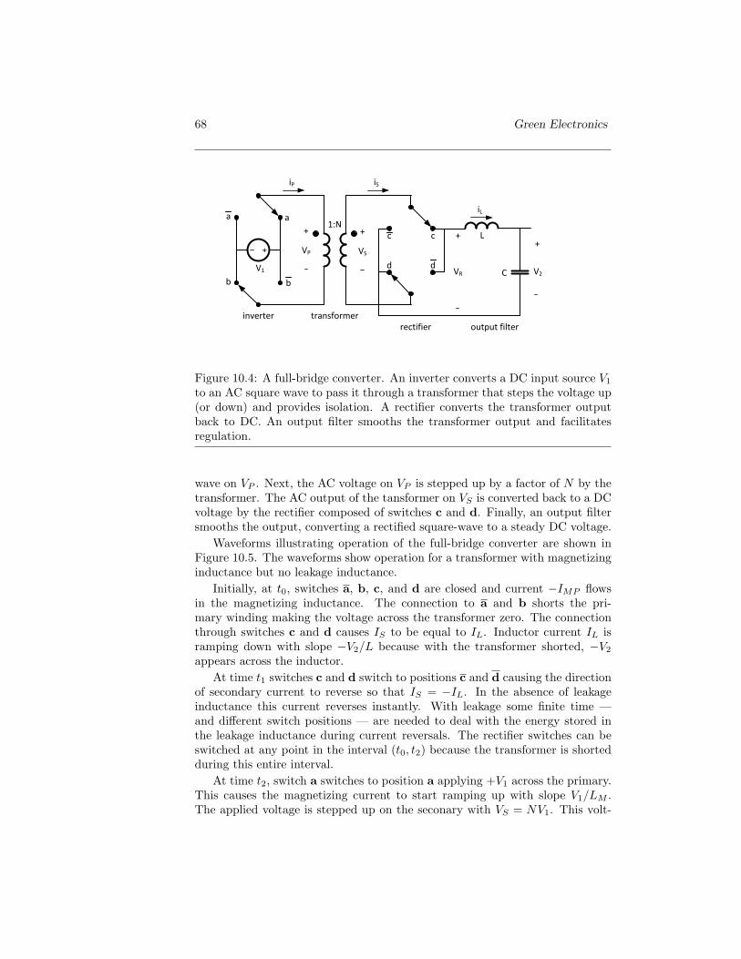
68 Green Electronics
1:N
iP
VP
+
inverter
V1+
b b
aa
transformer
d d
c c
V2
+L
iS
iL
rectifier output filter
C
VS
+
VR
+
Figure 10.4: A full-bridge converter. An inverter converts a DC input source V1
to an AC square wave to pass it through a transformer that steps the voltage up(or down) and provides isolation. A rectifier converts the transformer outputback to DC. An output filter smooths the transformer output and facilitatesregulation.
wave on VP . Next, the AC voltage on VP is stepped up by a factor of N by thetransformer. The AC output of the tansformer on VS is converted back to a DCvoltage by the rectifier composed of switches c and d. Finally, an output filtersmooths the output, converting a rectified square-wave to a steady DC voltage.
Waveforms illustrating operation of the full-bridge converter are shown inFigure 10.5. The waveforms show operation for a transformer with magnetizinginductance but no leakage inductance.
Initially, at t0, switches a, b, c, and d are closed and current −IMP flowsin the magnetizing inductance. The connection to a and b shorts the pri-mary winding making the voltage across the transformer zero. The connectionthrough switches c and d causes IS to be equal to IL. Inductor current IL isramping down with slope −V2/L because with the transformer shorted, −V2
appears across the inductor.At time t1 switches c and d switch to positions c and d causing the direction
of secondary current to reverse so that IS = −IL. In the absence of leakageinductance this current reverses instantly. With leakage some finite time —and different switch positions — are needed to deal with the energy stored inthe leakage inductance during current reversals. The rectifier switches can beswitched at any point in the interval (t0, t2) because the transformer is shortedduring this entire interval.
At time t2, switch a switches to position a applying +V1 across the primary.This causes the magnetizing current to start ramping up with slope V1/LM .The applied voltage is stepped up on the seconary with VS = NV1. This volt-

Copyright (c) 2011-14 by W.J Dally, all rights reserved 69
ba a b
V1
-V1
0VP
IM 0
IL0
Iavg
IS 0
Iavg
-Iavg
c ccswitch
t1 t2 t3t0 t4 t5 t6 t7
IMP
-IMP
NV1
0VR
Figure 10.5: Waveforms showing operation of the full-bridge converter of Fig-ure 10.4.

70 Green Electronics
age causes the current in the output inductor to start ramping up with slope(NV1 − V2) /L.
At time t3, switch b switches to position b again shorting the primary wind-ing. With no applied primary voltage the magnetizing current levels off at IMP .Shorting the primary also causes the secondary to be shorted causing the outputcurrent to ramp down with slope −V2/L — the same as at time t0.
The transitions at t4, t5, and t6 are identical to the transitions at t1, t2,and t3 but with the transformer polarity reversed. A negative voltage is appliedacross the primary. This gives a negative voltage across the secondary, and therectifier is switched in the opposite direction to give a positive voltage VR acrossthe output filter. The rectified volage VR across the output filter is the same att4, t5, and t6 as at t1, t2, and t3.
The output filter acts just like the inductor and capacitor in a buck converter.The rectified secondary voltage VR is a square wave with magnitude NV1 andduty factor D = (π − φab) /π, where φab is the phase difference between theoperation of switches a and b. Thus, as with a buck converter, the outputvoltage in periodic steady state is given by
V2 = DNV1 (10.23)
The transformer steps up the voltage by a factor of N and the output filteracts like a buck converter and steps it down by the duty factor D.
10.4 Effect of Leakage Inductance
Figure 10.6 shows waveforms illustrating the operation of the full-bridge con-verter of Figure 10.4 including the effects of leakage inductance. This operationrequires operating switches c and d so that both sides of each switch are closedsimultaneously, shorting both the transformer secondary and providing a cur-rent path for the output filter. This state is denoted by part of the c waveformwhere the signal is shown both high and low — indicating that both the c andc switches are closed at the same time (and similarly for switch d).
Consider the sequency of events starting at t1 when switch a turns on andboth sides of switches c and d are turned on. The input voltage V1 is appliedacross the primary by switches a and b and the secondary is shorted by switchesc and d. This applies the full input voltage V1 across the leakage inductance LL
and the transformer current ramps upward from its original negative state. Thisis reflected in the rise of IS with slope V1/NLL. The slope of IP (not shown)is V1/LL and the secondary current is stepped down by 1/N . With switches cand d also closed, a voltage of −V2 is across the output inductor and its currentramps down with slope −V2/L.
With all four rectifier switches closed, the transformer current is momentarilydecoupled from the output inductor current. This decoupling is necessary toallow time for the current in the leakage inductance to reverse. During thiscommutation period the transformer current rises through zero until at t2 IS =

Copyright (c) 2011-14 by W.J Dally, all rights reserved 71
b
a
V1
-V1
0VP
IM 0
IL0
Iavg
IS 0
Iavg
-Iavg
c
t1 t3t0 t4 t5 t6 t7
IMP
-IMP
NV1
0VR
t2
Figure 10.6: Waveforms showing operation of the full-bridge converter of Fig-ure 10.4 including the effects of leakage inductance.
72 Green Electronics
IL. At this point switches c and d open and the transformer current and outputinductor current are coupled with both positive. The delay due to leakageinductance tL from t1 to t2 is given by
tL =NLLILV1
(10.24)
where IL is the average output inductor current during this period.At t2 only a small fraction of the input voltage is being dropped across LL, so
most of the voltage appears across the transformer causing VS ,and hence VR toapproach NV1. This causes the output current, and secondary current becausethey are coupled, to ramp up with slope (NV1 − V2) /L. Also at t2 the trans-former voltage appears across the magnetizing inductance and the magnetizingcurrent IM ramps upward with slope V1/LM .
At time t3 switch b moves to position b and the transformer primary isshorted. This is reflected instantly across the transformer, since there is no delaydue to LL and VS and VR fall to zero at the same time. With no transformervoltage the magnetizing current levels at IMP and the output inductor currentIL starts ramping downward with slope −V2/L.
At time t4 the process repeats in the opposite direction. All four rectifierswitches are closed — shorting the secondary and decoupling the secondary andoutput currents. At the same time switch a switches to position a applying −V1
across the leakage inductance. After the leakage current ramps down to match−IL switches c and d open unclamping the secondary and re-coupling −IS withIL.
Each half-cycle, a voltage pulse with width tP = t3−t1 = t6−t4 is applied tothe primary. The first tL of each pulse is used to turn the current in the leakageinductance around. The remaining tS = tP − tL = t3 − t2 transfers energy tothe output inductor. It is the duty factor of the secondary DS = 2tS/tcy thatdetermines the output voltage according to (10.23).
10.5 Final Comments
Because the full-bridge converter is really just a buck converter with an isolatedstep-up (or down) input stage, controlling the full-bridge converter is essentiallythe same as controlling the buck. With a few adjustments to account for thetransformer ratio and for the leakage delay tL, the methods of Chapter 5 canbe applied to the full-bridge converter. We leave the details as an exercise.
In a practical full-bridge converter isolation of the control circuit is an issue.The controller is typically referenced to the secondary because it senses thesecondary voltage. The signals controlling the primary-side switches are passedthrough isolators to cross the unknown input-output voltage shift.
At first glance it might appear that timing of the switches would be difficultsince the secondary switches need to change state exactly at the point when thecurrent in the leakage inductor matches the current in the output inductor. In

Copyright (c) 2011-14 by W.J Dally, all rights reserved 73
practice this critical timing is performed automatically by diodes. Even in low-voltage systems that use MOSFETs for the secondary switches (synchronousrectification Section ??) diodes associated with the MOSFETs perform the ini-tial switching. The MOSFET then turns on to reduce the voltage drop.
10.6 Exercises
transformer with more than two windingssolve Figure 10.2 using equationssolve some other xfmr examplesmatlab sim of bridge convertercontrol of bridge converter

74 Green Electronics

Chapter 11
The Flyback Converter
The flyback converter is interesting because it uses the magnetizing inductanceof the transformer for energy storage. This is fundamentally different than theother isolated converters for which the magnetizing inductance is a parasiticelement. The productive use of the magnetizing inductance allows a flybackconverter to be built with a single magnetic component that serves both as anisolating transformer and as the energy storage element. In contrast most otherisolated converters require a separate storage inductor (like the output filterinductor in Figure 10.4) in addition to the transformer.
11.1 Flyback Topology and Operation
Figure 11.1 shows a schematic diagram of a flyback converter. The converteris quite simple consisting just of a transformer, two switches, and an outputcapacitor. Because of its importance we draw the magnetizing LM inductanceexplicitly. This is not a separate component but rather part of the transformer.
Operation of the flyback converter is controlled by the two switches whichclose alternately. When switch a is closed input supply V1 is connected acrossLM and current iM ramps up. In this phase of operation iM flows around aloop that includes switch a and the input supply. Because switch b is open nocurrent flows through the ideal transformer.
When switch a opens and switch b closes current iM flows in a loop betweenLM and the primary winding. This induces a current in the secondary windingthat charges output capacitor C. During this period voltage V2 is applied acrossthe secondary, −V2/N is reflected to the primary, and iM ramps down.
Figure 11.2 shows waveforms for the flyback converter illustrating how themagnetizing current iM alternates between the primary and secondary circuits.When switch a is closed, primary current iP is equal to magnetizing current iMboth of which ramp upward with slope V1
L because the input supply is appliedacross LM .
When switch b is closed (and a is open) iP is zero and iM flows through
75

76 Green Electronics
1:N
VS
+
LM
a
+
C V2
b
V1
+
iM VP
+
iP
iS
Figure 11.1: A flyback converter stores energy in the magnetizing inductance ofthe transformer LM .
the secondary circuit. During this phase iS = iM
N . The reflected and invertedsecondary voltage −V2
N appears across LM causing iM to ramp downward withslope − V2
NL . Secondary current, being scaled by 1/N ramps with slope − V2N2L .
In the periodic steady state the volt-seconds across LM must balance andwe have:
DV1 = (1−D)V2
N(11.1)
Where D is the duty factor of switch a. Rewriting this gives the relation:
V2 =ND
1−DV1 (11.2)
This is similar to the relationship for the buck-boost converter (6.6) but multi-plied by the transformer turns ratio.
When the converter is not in the periodic steady state, the change in mag-netizing current and capacitor voltage each cycle are given by:
∆ii =tcy (DNV1 − (1−D)vi)
NL(11.3)
∆vi =tcy (1−D) ii −NiLoad
NC(11.4)
Converting to Laplace transforms gives:

Copyright (c) 2011-14 by W.J Dally, all rights reserved 77
a
b
iM
VP 0
V1
-V2
N
iP
iS
Figure 11.2: Waveforms showing operation of the flyback converter of Fig-ure 11.1. When switch a is closed input supply V1 is across LM and mag-netizing current iM ramps up. When a opens and b closes LM discharges itsenergy through the transformer into capacitor C and iM ramps down.
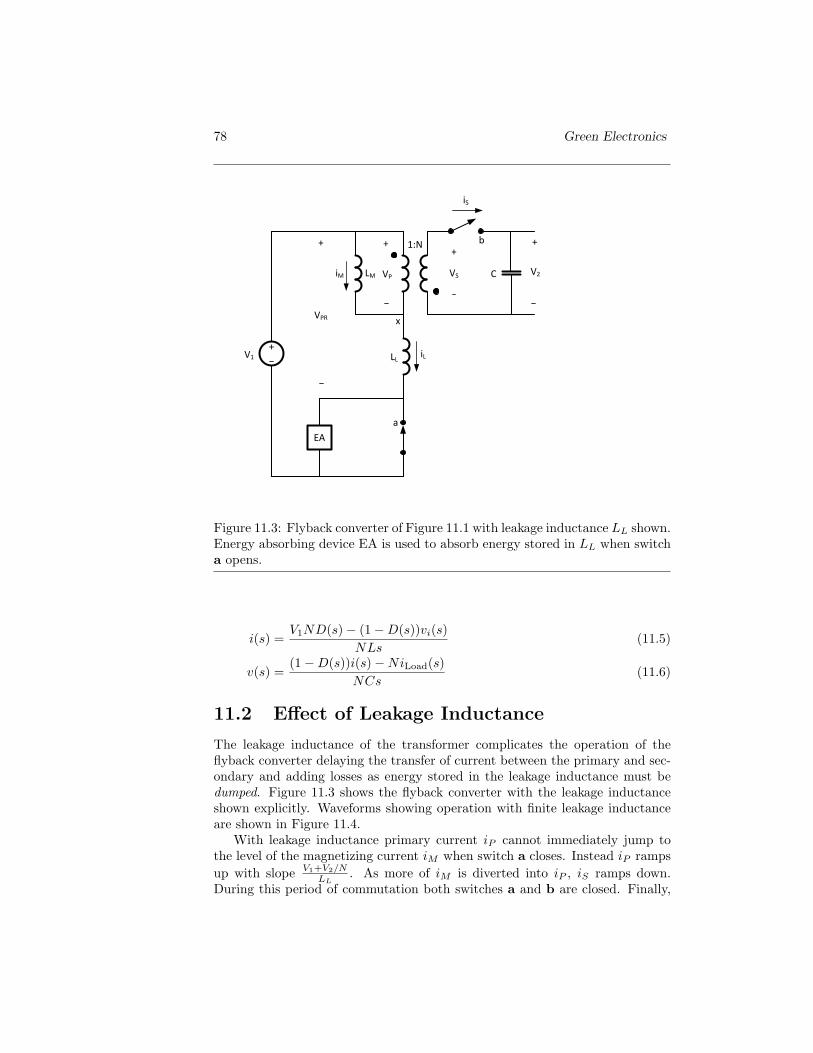
78 Green Electronics
1:N
VS
+
LM
a
+
C V2
b
V1
+
iM VP
+
LL iL
x
EA
iS
VPR
+
Figure 11.3: Flyback converter of Figure 11.1 with leakage inductance LL shown.Energy absorbing device EA is used to absorb energy stored in LL when switcha opens.
i(s) =V1ND(s)− (1−D(s))vi(s)
NLs(11.5)
v(s) =(1−D(s))i(s)−NiLoad(s)
NCs(11.6)
11.2 Effect of Leakage Inductance
The leakage inductance of the transformer complicates the operation of theflyback converter delaying the transfer of current between the primary and sec-ondary and adding losses as energy stored in the leakage inductance must bedumped. Figure 11.3 shows the flyback converter with the leakage inductanceshown explicitly. Waveforms showing operation with finite leakage inductanceare shown in Figure 11.4.
With leakage inductance primary current iP cannot immediately jump tothe level of the magnetizing current iM when switch a closes. Instead iP rampsup with slope V1+V2/N
LL. As more of iM is diverted into iP , iS ramps down.
During this period of commutation both switches a and b are closed. Finally,
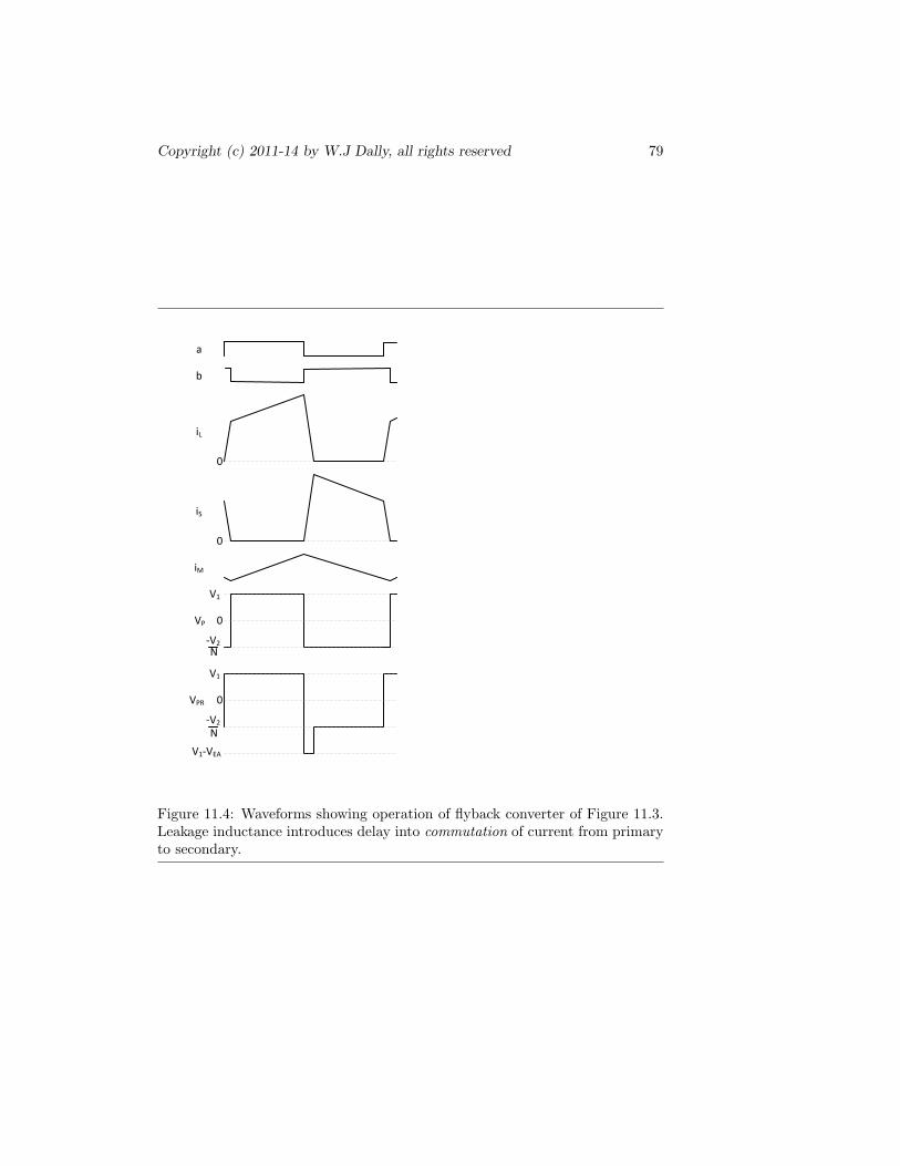
Copyright (c) 2011-14 by W.J Dally, all rights reserved 79
a
b
iM
VP 0
V1
-V2
N
iL
0
iS
0
VPR 0
V1
-V2
N
V1-VEA
Figure 11.4: Waveforms showing operation of flyback converter of Figure 11.3.Leakage inductance introduces delay into commutation of current from primaryto secondary.

80 Green Electronics
when iS reaches zero, switch b opens and the flyback operates as in Figure 11.2until switch a opens. Because the input voltage V1 is not applied across themagnetizing inductance until iL reaches iM the effective pulse width is reducedby the delay of the ramp.
When switch a opens the leakage current is directed into an energy absorber(EA). The voltage across EA must be greater than V1 +V2/N to decrease iL. Inpractice the energy absorber is often the MOSFET used for switch a operatingin its avalanche breakdown region (Section ??). The energy lost by dumping iLinto EA is at least the leakage energy EL = i2LLL/2 itself and may be greater.Some flyback converters use methods to recover this leakage energy. One suchmethod is described in Section 11.3.
As iL ramps down — dumping its energy into EA — the balance of iM(scaled by 1/N) flows into iS . When iL reaches zero, iS reaches iM/N .
The bottom two traces of Figure 11.4 show the ideal primary voltage VP
and the real primary voltage VPR, which includes the drop across the leakageinductance. These two traces differ during the periods where iL is rampingrapidly to commutate the current between primary and secondary. When switcha first turns on VP is −V2/N while VPR is V1. This applies V1 + V2/N acrossLL to ramp iL upward. When switch a turns off VP is again −V2/N while VPR
is V1 − VEA applying VEA − V1 − V2/N in the opposite direction across LL toramp iL downward.
11.3 Diagonal Flyback
The energy stored in the leakage inductance can be recycled to the input supplyby adding three switches to the flyback converter as shown in Figure 11.5. Asecond a switch is added to isolate the top of the primary from the input supplywhen a turns off. Two c switches are added to connect the primary backwardsacross the input supply to recover leakage energy.
During the middle of the waveforms in Figure 11.4 when switch a turns offand b turns on, switch c also turns on just long enough for the leakage energyto be returned to the input supply. During this period, with switch b closed,V2 appears across VS and is reflected as −V2/N across VP . With the bottomc switch closed this places point x at V2/N . For the leakage current to reducewe must have V1 > V2/N . Then the voltage across the leakage inductanceis V1 − V2/N and iL ramps down with slope NV1−V2
NLL. When iL reaches zero
switches c turn off.
The c switches are typically implemented as a pair of diodes with the cath-odes up. This makes their timing automatic. When switches a open the flowof leakage current forward biases diodes c turning them on. When the leakagecurrent reaches zero (i.e., when all of the magnetizing current is flowing to thesecondary) the diodes turn off.

Copyright (c) 2011-14 by W.J Dally, all rights reserved 81
1:N
VS
+
LM
a+
C V2
b
V1
+
iM VP
+
LL iL
x
iS
a
c
c
VPR
+
Figure 11.5: A diagonal flyback converter recycles energy in the leakage induc-tance to the input supply.

82 Green Electronics
11.4 Primary-Side Sensing
One advantage of the flyback converter is that the output voltage can be sensedon the primary side. This allows the converter to be controlled entirely from theprimary side — without the need for an optocoupler, or other isolation device,to communicate control signals across the transformer.
When switch b is closed, output voltage V2 appears directly across the sec-ondary and is reflected so that −V2/N appears across the primary. This scaledversion of the output voltage can be sensed after the leakage current has stoppedflowing. Alternately an auxiliarly winding can be added to the transformer al-lowing the secondary voltage to be sensed any time switch b is closed.
11.5 Exercises
give some component values calculate slopes and give waveformsmatlab simulationcontroller

Chapter 12
Other Isolated Converters
There are many types of isolated converters. We can remove half of the primaryside switches giving a half-bridge converter. Moving the inductor to the pri-mary gives a current-fed bridge converter — and isolated version of the boostconverter. We can operate on only one half-cycle giving a forward converter.We can center-tap the input or output winding of the transformer. The listgoes on. We leave the treatment of most of these topologies to a later sectionbecause they are small variations
83

84 Green Electronics
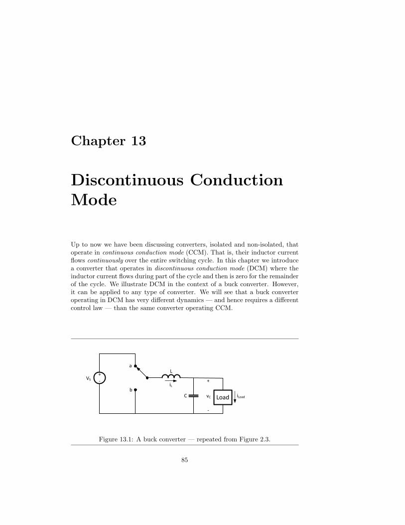
Chapter 13
Discontinuous ConductionMode
Up to now we have been discussing converters, isolated and non-isolated, thatoperate in continuous conduction mode (CCM). That is, their inductor currentflows continuously over the entire switching cycle. In this chapter we introducea converter that operates in discontinuous conduction mode (DCM) where theinductor current flows during part of the cycle and then is zero for the remainderof the cycle. We illustrate DCM in the context of a buck converter. However,it can be applied to any type of converter. We will see that a buck converteroperating in DCM has very different dynamics — and hence requires a differentcontrol law — than the same converter operating CCM.
L
iL
VS
+
-
a
bvC Load
+
-
C iLoad
Figure 13.1: A buck converter — repeated from Figure 2.3.
85
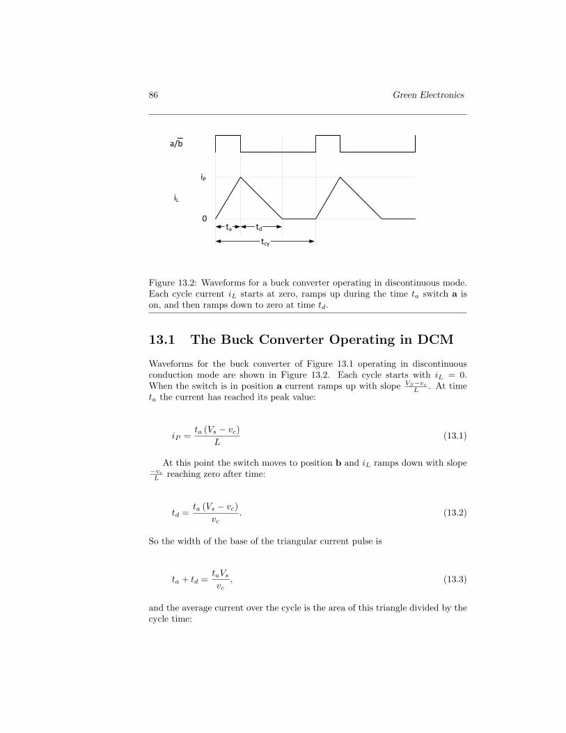
86 Green Electronics
a/b
iL
0
iP
td
tcy
ta
Figure 13.2: Waveforms for a buck converter operating in discontinuous mode.Each cycle current iL starts at zero, ramps up during the time ta switch a ison, and then ramps down to zero at time td.
13.1 The Buck Converter Operating in DCM
Waveforms for the buck converter of Figure 13.1 operating in discontinuousconduction mode are shown in Figure 13.2. Each cycle starts with iL = 0.When the switch is in position a current ramps up with slope VS−vc
L . At timeta the current has reached its peak value:
iP =ta (Vs − vc)
L(13.1)
At this point the switch moves to position b and iL ramps down with slope−vc
L reaching zero after time:
td =ta (Vs − vc)
vc. (13.2)
So the width of the base of the triangular current pulse is
ta + td =taVs
vc, (13.3)
and the average current over the cycle is the area of this triangle divided by thecycle time:

Copyright (c) 2011-14 by W.J Dally, all rights reserved 87
if(i_l < 0) % in discontinuous mode no negative currenti_l = 0 ;
end
Figure 13.3: To simulate a buck converter in discontinuous mode we add thisif statement to the code of Figure 4.1 to prevent iL from going negative.
iL =t2aVS (Vs − vc)
2Ltcyvc, (13.4)
=tcyD
2VS (Vs − vc)2Lvc
. (13.5)
In contrast to the buck operating in continuous condition mode (CCM) (Fig-ure 3.1), in DCM iL starts each cycle at zero. (13.5) shows that the averagecurrent over a cycle iL varies directly with D2, the square of duty factor. Incontrast, in CCM, the derivative of the current varies linearly with D.
Discontinuous mode results when switch b is realized as a diode (or a MOS-FET controlled to act like a diode) at low currents and low pulse widths.
13.2 Simulation
To simulate the buck converter in discontinuous mode, we simply add the ifstatement shown in Figure 13.3.
[More]
13.3 Control
To develop a control law for the buck operating in DCM we linearize (13.5) bydefining a control variable x = D2 giving:
iL =tcyxVS (Vs − vc)
2Lvc. (13.6)
If we assume vc is a constant VC for the purposes of control, this is just asimple linear dependance of iL = Kx . The voltage just integrates this:
v(s) =iL(s)Cs
(13.7)
=x(s)Ks
(13.8)
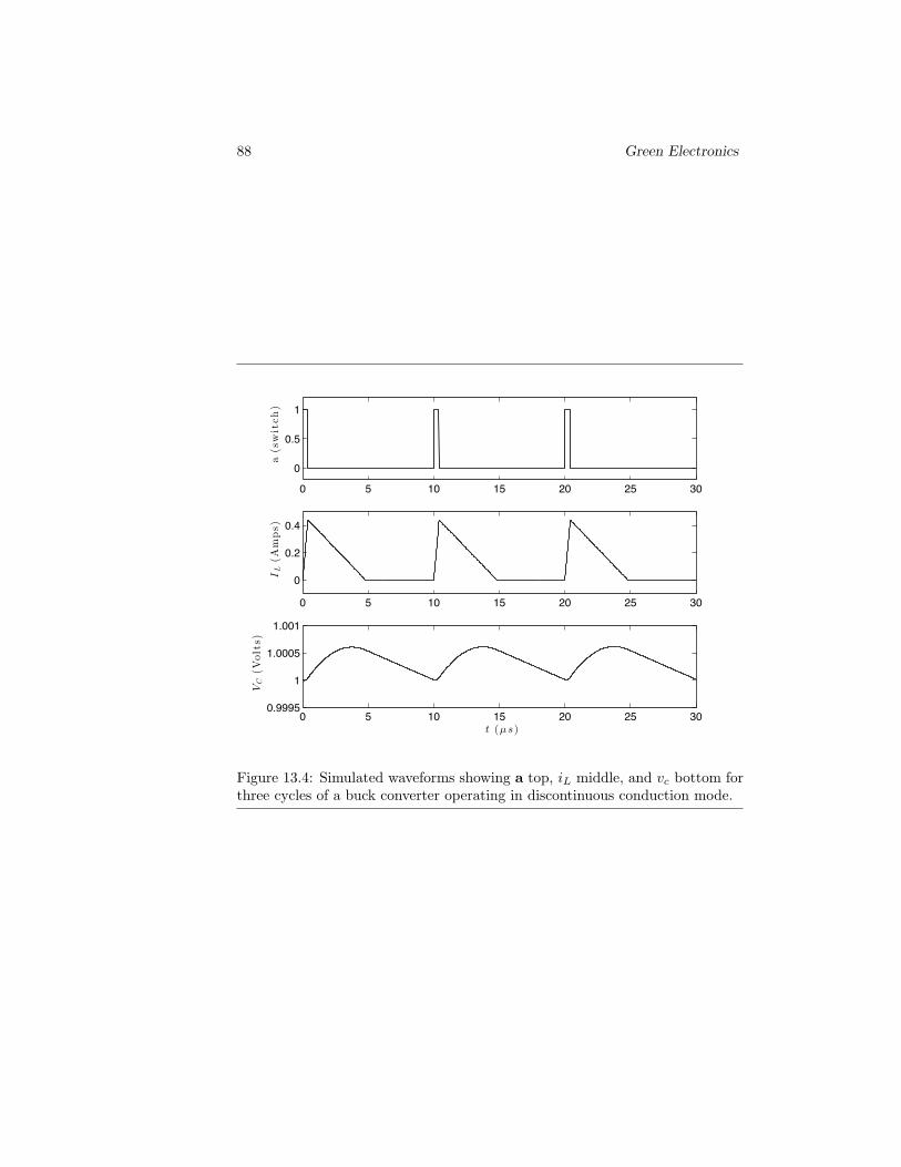
88 Green Electronics
0 5 10 15 20 25 30
0
0.5
1
a(switch)
0 5 10 15 20 25 30
0
0.2
0.4
IL(A
mps)
0 5 10 15 20 25 300.9995
1
1.0005
1.001
VC(V
olts)
t (µ s)
Figure 13.4: Simulated waveforms showing a top, iL middle, and vc bottom forthree cycles of a buck converter operating in discontinuous conduction mode.

Copyright (c) 2011-14 by W.J Dally, all rights reserved 89
Where gain constant K is given by
K =tcyVS (Vs − Vc)
2LCVc. (13.9)
Note that because gain K depends strongly on Vc we may need to change ourcontrol parameters as Vc changes.
To control this simple first-order system we can use a PI controller wherethe control law is
x(s) =(P +
Q
s
)e(s) (13.10)
The open-loop response is
H(s) =KPs+KQ
s2, (13.11)
and the closed loop response is
G(s) =H(s)
1 +H(s)(13.12)
=KPs+KQ
s2 +KPs+KQ(13.13)
So the natural frequency and damping factor are given by
ω =√KQ (13.14)
ζ =KP
2ω(13.15)
We can solve these equations for our controller gains:
Q =ω2
K(13.16)
P =2 ∗ zeta ∗ omega
K(13.17)
Using the parameters from Chapter 5 and choosing ω = 3 × 10⁴ and ζ = 1we get P = 0.91 and Q = 1.36× 10⁴.
The Matlab code for our linearized PI controller is shown in Figure 13.5.This code determines the voltage error er and integrates this error to give anintegral error ier. These two error terms are combined using the proportionaland integral gains P and Q to generate linear control variable x. After limitingx we take its square root to give duty factor and multiply by t c to give pulsewidth.
The simulated response of the controller is showin in Figure 13.6.[More]

90 Green Electronics
% linearized PI control law - run once per cycleer = v_ref - v_c ;ier = ier + er*t_c ;x = (er*P + ier*Q) ;x = max(0, min(x_max, x)) ;t_a = t_c*sqrt(x) ;
Figure 13.5: Matlab implementation of linearized PI controller for a discontin-uous mode buck converter.
0 100 200 300 400 500 600 700 800 9000
0.20.40.6
i L(A
mps)
0 100 200 300 400 500 600 700 800 900
0.998
1
1.002
vC(V
olts)
0 100 200 300 400 500 600 700 800 9000
0.20.40.6
t a(µ
s)
t (µ s)
Figure 13.6: Simulated waveforms showing control of a buck converter in discon-tinuous mode. Waveforms show iL (top), vC (middle), and ta (bottom). iLoad
is initially 0.1A, steps up to 0.2A at 30µs, and steps down to 0.05A at 60µs.

Copyright (c) 2011-14 by W.J Dally, all rights reserved 91
13.4 Exercises
boost dcmflyback dcm

92 Green Electronics

Chapter 14
Capacitive Converters
Most switched voltage converters use inductors as their primary energy storageelement. This is because the voltage at the terminals of an inductor can beswitched quickly. An inductor holds its current constant but can have its voltageswitched to transfer energy from one voltage to another.
We can also use capacitors to build voltage converters by charging a capacitorat one voltage and then switching its terminals to change a parallel connection toa series connection or vice-versa. With this approach we are limited to rationalratios of input to output voltage. Also, even with ideal switches capacitiveconverters have losses.
14.1 A Capacitive Voltage Doubler
The circuit shown in Figure 14.1 is a capacitive voltage doubler. Each cyclecapacitor C1 is charged to the input voltage and then lifted up so that its topterminal is at twice the input voltage. This doubled voltage is stored on outputcapacitor C2 where it is drained off by the load before being replenished duringthe next cycle.
When the two switches are in position a input source VS is connected acrosscapacitor C1 and capacitor C1 is charged to VS . Because real switches havefinite resistance RS this takes a finite amount of time (given by a τ = RSC1
time constant) and even if ta is many τ the voltage on C1 doesn’t quite reachVS .
When the switches move to position b C1 which is now charged to VS has itsnegative terminal connected to the positive terminal of the supply. That putsC1 and VS in series. The voltage across the series combination of VS and C1 ismomentarily 2VS .
The upper switch in position b connects the series combination of VS and C1
in parallel with output capacitor C2 and current will flow to redistribute chargeuntil VS + VC1 = VC2.
93
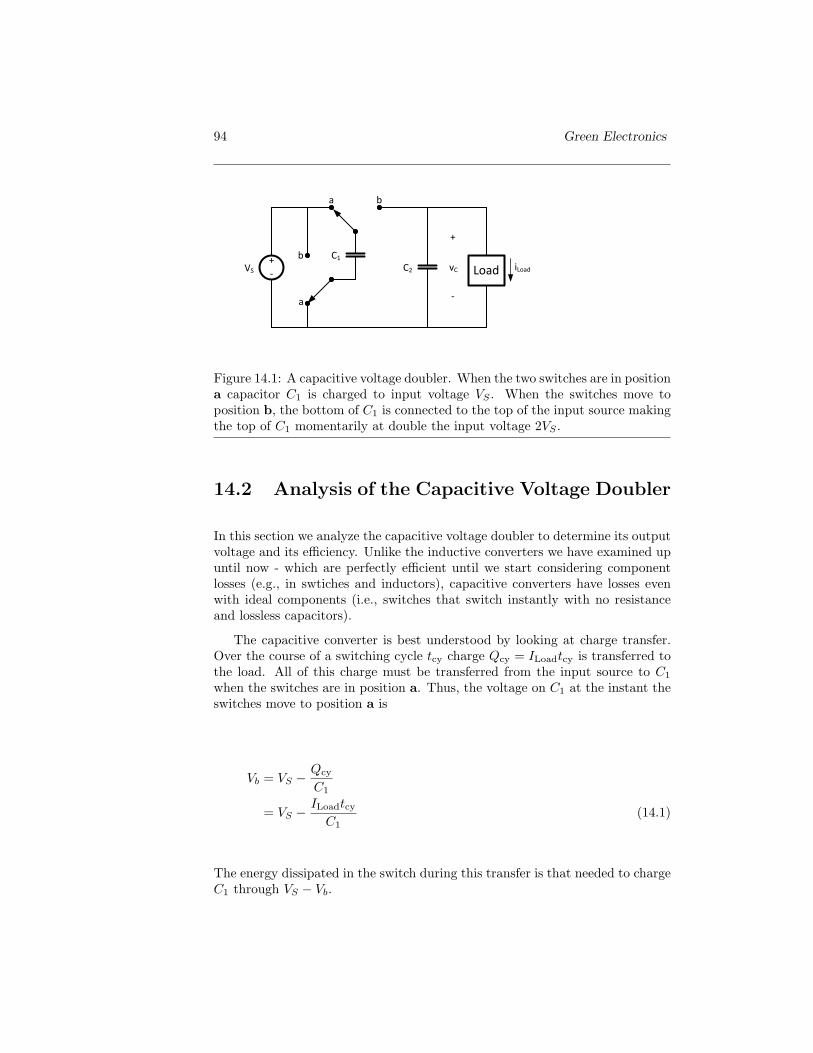
94 Green Electronics
VS
+
-
C1C2
a b
a
bvC Load
+
-
iLoad
Figure 14.1: A capacitive voltage doubler. When the two switches are in positiona capacitor C1 is charged to input voltage VS . When the switches move toposition b, the bottom of C1 is connected to the top of the input source makingthe top of C1 momentarily at double the input voltage 2VS .
14.2 Analysis of the Capacitive Voltage Doubler
In this section we analyze the capacitive voltage doubler to determine its outputvoltage and its efficiency. Unlike the inductive converters we have examined upuntil now - which are perfectly efficient until we start considering componentlosses (e.g., in swtiches and inductors), capacitive converters have losses evenwith ideal components (i.e., switches that switch instantly with no resistanceand lossless capacitors).
The capacitive converter is best understood by looking at charge transfer.Over the course of a switching cycle tcy charge Qcy = ILoadtcy is transferred tothe load. All of this charge must be transferred from the input source to C1
when the switches are in position a. Thus, the voltage on C1 at the instant theswitches move to position a is
Vb = VS −Qcy
C1
= VS −ILoadtcyC1
(14.1)
The energy dissipated in the switch during this transfer is that needed to chargeC1 through VS − Vb.

Copyright (c) 2011-14 by W.J Dally, all rights reserved 95
Eb =12C1 (VS − Vb)
2
=Q2
cy
C1
=(ILoadtcy)
2
C1(14.2)
While the switch is in position a the load continues to discharge C2. At theend of the cycle, just before switching to position b the voltage on C2 is
Vc = Vb −ILoadtaC2
(14.3)
Where ta is the time in switch position a.When the switch moves to position b capacitor C2 which is charged to Vc
shares charge with C1 which is charged to VS . The resulting voltage Va is givenby adding the voltage drop during tb to Vb.
Va = Vb +ILoadtbC1 + C2
(14.4)
Which is also equal to the voltage given by the charge sharing
Va =C1VS + C2Vc
C1 + C2(14.5)
During this charge sharing the energy dissipated in the switch is given by
Ea =C1C2 (VS − Vc)
2
C1 + C2
=C1C2
(ILoadtcy
C1+ ILoadta
C2
)2
C1 + C2
=I2Load (C2tcy + C1ta)2
C1C2 (C1 + C2)(14.6)
So the total energy lost each cycle is
Ecy = Eb + Ea
=(ILoadtcy)
2
C1+I2Load (C2tcy + C1ta)2
C1C2 (C1 + C2)
= I2Load
(t2cyC1
+(C2tcy + C1ta)2
C1C2 (C1 + C2)
)(14.7)

96 Green Electronics
So we see that the inherent energy loss of the capacitive converter increasesquadratically with load current ILoad and is inversely proportional to the ca-pacitance. The energy increases quadratically with cycle time tcy; so powerincreases linearly with tcy.
One way to think about this power loss is that its just the load currenttimes the instantaneous voltage drop between VS and V2. With ideal circuitelements, if we pick C1 and C2 so that average voltage drop is about 10%,the converter will be about 90% efficient1 This is in contrast to an inductiveconverter which, with ideal elements, is 100% efficient. Because of this inherentefficiency disadvantage, capacitive converters are rarely used when efficiencymatters unless inductors are not available.
14.3 Exercises
Capacitive voltage halverCapacitive voltage negaterMultiply by 3/2
1A real converter, however will have many other losses and will not be anywhere near thisefficient.
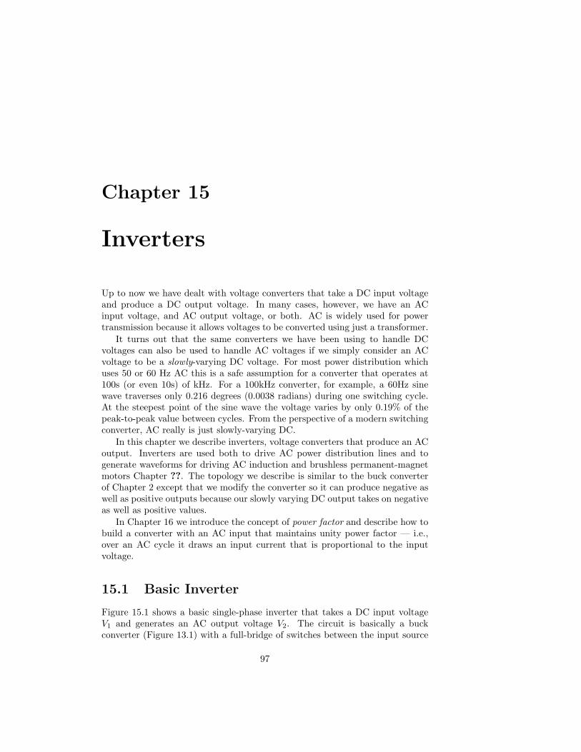
Chapter 15
Inverters
Up to now we have dealt with voltage converters that take a DC input voltageand produce a DC output voltage. In many cases, however, we have an ACinput voltage, and AC output voltage, or both. AC is widely used for powertransmission because it allows voltages to be converted using just a transformer.
It turns out that the same converters we have been using to handle DCvoltages can also be used to handle AC voltages if we simply consider an ACvoltage to be a slowly-varying DC voltage. For most power distribution whichuses 50 or 60 Hz AC this is a safe assumption for a converter that operates at100s (or even 10s) of kHz. For a 100kHz converter, for example, a 60Hz sinewave traverses only 0.216 degrees (0.0038 radians) during one switching cycle.At the steepest point of the sine wave the voltage varies by only 0.19% of thepeak-to-peak value between cycles. From the perspective of a modern switchingconverter, AC really is just slowly-varying DC.
In this chapter we describe inverters, voltage converters that produce an ACoutput. Inverters are used both to drive AC power distribution lines and togenerate waveforms for driving AC induction and brushless permanent-magnetmotors Chapter ??. The topology we describe is similar to the buck converterof Chapter 2 except that we modify the converter so it can produce negative aswell as positive outputs because our slowly varying DC output takes on negativeas well as positive values.
In Chapter 16 we introduce the concept of power factor and describe how tobuild a converter with an AC input that maintains unity power factor — i.e.,over an AC cycle it draws an input current that is proportional to the inputvoltage.
15.1 Basic Inverter
Figure 15.1 shows a basic single-phase inverter that takes a DC input voltageV1 and generates an AC output voltage V2. The circuit is basically a buckconverter (Figure 13.1) with a full-bridge of switches between the input source
97
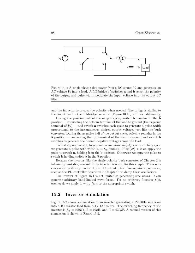
98 Green Electronics
V1
+
b
b
a
a
L
iL
V2 Load
+
-
C
Figure 15.1: A single-phase takes power from a DC source V1 and generates anAC voltage V2 into a load. A full-bridge of switches a and b select the polarityof the output and pulse-width-modulate the input voltage into the output LCfilter.
and the inductor to reverse the polarity when needed. The bridge is similar tothe circuit used in the full-bridge converter (Figure 10.4) just drawn differently.
During the positive half of the output cycle, switch b remains in the bposition — connecting the bottom terminal of the load to ground (the negativeterminal of V1) — and switch a switches each cycle to generate a pulse widthproportional to the instantaneous desired output voltage, just like the buckconverter. During the negative half of the output cycle, switch a remains in thea position — connecting the top terminal of the load to ground and switch bswitches to generate the desired negative voltage across the load.
To first approximation, to generate a sine wave sin(ωt), each switching cyclewe generate a pulse with width tp = tcy| sin(ωt)|. If sin(ωt) > 0 we apply thepulse to switch a, holding b in the b position. Otherwise we appy the pulse toswitch b holding switch a in the a postion.
Because the inverter, like the single-polarity buck converter of Chapter 2 isinherently unstable, control of the inverter is not quite this simple. Transientscan excite oscillitory modes of the LC output filter. We require a controller,such as the PD controller described in Chapter 5 to damp these oscillations.
The inverter of Figure 15.1 is not limited to generating sine waves. It cangenerate arbitrary band-limited wave forms. For an arbitrary function f(t),each cycle we apply tp = tcy|f(t)| to the appropriate switch.
15.2 Inverter Simulation
Figure 15.2 shows a simulation of an inverter generating a 1V 60Hz sine waveinto a 1Ω resistor load from a 1V DC source. The switching frequency of theinverter is fcy = 60kHz, L = 10µH, and C = 630µF. A zoomed version of thissimulation is shown in Figure 15.3.
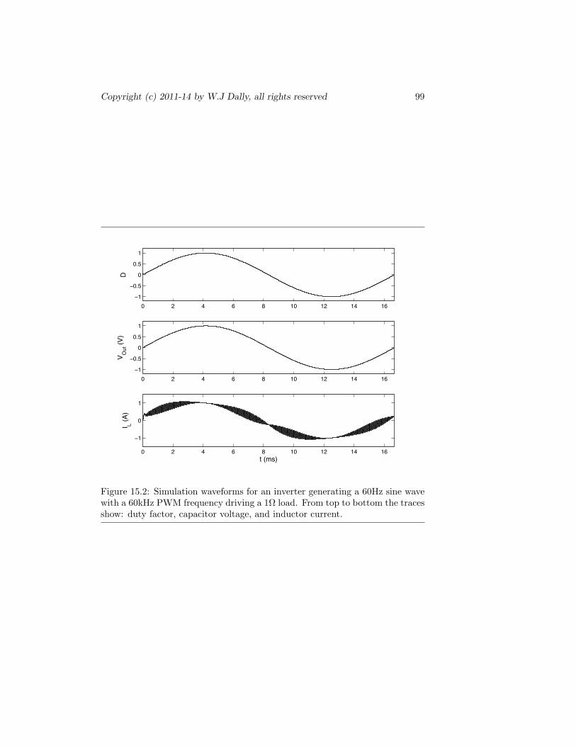
Copyright (c) 2011-14 by W.J Dally, all rights reserved 99
0 2 4 6 8 10 12 14 16−1
−0.5
0
0.5
1
D
0 2 4 6 8 10 12 14 16−1
−0.5
0
0.5
1
V Out
(V)
0 2 4 6 8 10 12 14 16
−1
0
1
I L (A)
t (ms)
Figure 15.2: Simulation waveforms for an inverter generating a 60Hz sine wavewith a 60kHz PWM frequency driving a 1Ω load. From top to bottom the tracesshow: duty factor, capacitor voltage, and inductor current.

100 Green Electronics
1.68 1.7 1.72 1.74 1.76 1.78 1.8 1.82
0.58
0.6
0.62
0.64
D
1.68 1.7 1.72 1.74 1.76 1.78 1.8 1.82
0.58
0.6
0.62
0.64
V Out
(V)
1.68 1.7 1.72 1.74 1.76 1.78 1.8 1.820
0.5
1
1.5
I L (A)
t (ms)
Figure 15.3: Zoomed view of Figure 15.2 showing the region from 1.66ms to1.84ms.

Copyright (c) 2011-14 by W.J Dally, all rights reserved 101
101 102 103 104 105 106
−180
−160
−140
−120
−100
−80
−60
−40
−20
0
f (Hz)
Mag
(dB)
Figure 15.4: Spectrum of inverter output shows dominant peak at 60Hz. Thepeak at the switching freqeuncy is attenuated by the LC filter to -94dB.
The duty factor, shown in the top trace of each figure tracks the sine wave.Note, however, that this duty factor is not generated open loop, but is rather theoutput of a PD controller where sin(ωt) is the reference input to the controller.The center trace of each figure shows the voltage waveform accurately tracesthe desired sine wave to about 1% accuracy. There is a very small voltage rippleat the 60kHz switching frequency. The bottom trace shows that the inductorcurrent slightly leads the capacitor voltage — in order to charge and dischargethe capacitor. It has a ripple that peaks at nearly 0.4A but is almost zero atthe voltage peak - where the duty factor is 1.
In applications where an inverter generates a sine wave we one measure ofthe quality of the inverter is its spectral purity. Figure 15.4 shows the spectrumout of an inverter. The figure was generated by running the inverter simulationfor 32 cycles and taking an FFT of the resulting waveform across C. We haveincreased the value of C to 6.7mF to give an LC filter with a cutoff frequencyof fc ≈ 600Hz. We set the 0dB reference at the magnitude of this 1V tone.The noise floor at -155dB is determined by the length of the simulation (andthe FFT) and does not reflect any property of the inverter. The corner wherethis noise floor intersects the roll-off of the 60Hz harmonics does not reflect thecutoff frequency of the filter.

102 Green Electronics
There are two sets of lines of interest in this spectrum, the harmonics of the60Hz output tone, and the harmonics of the 60kHz switching frequency. The60Hz tone dominates the spectrum. Its first two odd harmonics (the third har-monic at 180Hz and the fifth at 300Hz) are about 90dB down. These harmonicscould be reduced by tighter regulation of the output voltage. The seventh andhigher odd harmonics are attenuated by the LC output filter.
The line at the 60kHz switching frequency is attenuated 80dB by the filter soit has a magnitude of -94dB. Both even and odd harmonics of the fundamentalappear in this group of lines and this chain of harmonics rolls off at the 40dBper decade of the LC filter.
In this chapter we have considered an inverter that is operating as a syn-thesizer, generating its own sine wave independently. In some cases we wish tobuild grid-tied inverters that generate an output waveform synchronized withthe AC grid. To build a grid-tied inverter we regulate not the output voltage —that is determined by the grid — but rather the output current. Such invertersgenerate a current that is proportional to the instantaneous grid voltage. Thisis an example of power-factor control which is the topic of the next chapter.
15.3 Exercises
matlab simulation of an inverterinverter that generates a triangle wavederive PD controller parameters for inverter with L = 10µH and C=2000µF.Design output filter to attenuate lines further
Chapter 16
Power Factor Correction
When connecting a device to an AC line it is often required that the devicecurrent be proportional to the line voltage. This is true whether the deviceis driving current into the AC line — e.g., a grid-tied inverter — or drawingcurrent from the line — e.g., an off-line voltage regulator. The requirement forcurrent-voltage proportionality is often described in terms of power factor, anumber that reflects the fraction of current that is at the same frequency andin phase with the voltage waveform.
To manage power factor, we again view the AC line as a slowly varyingDC source (or load) and regulate our current out of (or in to) the line to beproportional to the voltage. In many power converters this proportional currentcontrol is performed in a separate power factor correction input stage. For a grid-connected inverter, the inverter is controlled to provide a proportional outputcurrent.
16.1 Power Factor
Power factor is defined as the ratio of real power to apparent power averagedover an integral number of AC cycles. Apparent power here is the RMS value ofcurrent multiplied by the RMS value of voltage. If the instantanous voltage andcurrent at time t are v(t) and i(t) respectively we can calculate power factor as:
PF =P
VrmsIrms
=∫v(t)i(t)dt√∫
v2(t)dt√∫
i2(t)dt(16.1)
If an AC voltage source drives a load composed of passive linear circuitelements (resistors, capacitors, and inductors), then the current waveform willbe a sine wave at the line frequency and the power factor is determined by thephase angle θ between the voltage wave and the current wave, PF = cos(θ).
103

104 Green Electronics
0 2 4 6 8 10 12 14 16−1.5
−1
−0.5
0
0.5
1
1.5
t (ms)
i (A)
, v (V
)
101 102 103−100
−80
−60
−40
−20
0
f (Hz)
Mag
(dB)
Figure 16.1: Example non-sinusoidal current waveform is ±1A during 20% ofthe cycle and zero during the remainder of the cycle. The top trace showsthe voltage (dotted) and current (solid) waveforms. The bottom trace showsthe power spectrum of the current waveform normalized to its fundamentalmagnitude.
For example, if our load is an 2.7mF capacitor in parallel with a 1Ω resistor,then the admittance of the load is Y = 1/R + jωC, then for a 60Hz inputsource (ω = 2π × 60 = 377 rad/s) our admittance is Y = 1 + jf. which hasa magniude of
√(2) and an angle θ = pi/4. In this case the power factor is
PF = 2−1/2 = .707.For switching power converters we are usually less concerned about phase
shift in the line-frequency component of the current than we are with higher-frequency components of current. For example, some older power supplies rec-tified the AC input voltage and then connected the rectifier output to a filtercapacitor. Such power supplies draw current only during the part of the ACcycle when the input waveform is above the capacitor voltage. During the restof the cycle the input current is zero.
Consider the simplified current waveform shown in the top part of Fig-ure 16.1. The current is ±1A during 20% of the cycle and 0 during hte re-mainder of the cycle. The sinusoidal voltage waveform with RMS value of 1 isshown (dotted) for comparison. The power spectrum of the current waveform

Copyright (c) 2011-14 by W.J Dally, all rights reserved 105
is shown in the bottom panel of Figure 16.1. The spectrum shows significantpower in the odd harmonics of the current signal.
To compute the power factor of this signal (with the phase relationship tothe voltage signal as shown), we numerically perform the integrals in (16.1) andcompute
P = 0.28WIrms = 0.45AVrms = 1.0VPF = 0.62 (16.2)
Such a low power factor would be unacceptable in most power converters. Mostregulations require a power factor very close to one.
16.2 Power Factor Correction
[two stage converter figure]Many voltage converters use a power-factor-correction (PFC) input stage to
tailor their input current profile to match the AC voltage waveform. As shownin Figure ?? the converter consists of two stages. The input stage takes an AC(120V or 240V 50 or 60Hz) input and generates an intermediate DC voltage(often 400V DC) on a storage capacitor C. The output stage then convertsthis intermediate voltage to the output voltage (AC or DC) using one of theconverter topologies previously discussed. The output converter almost alwaysuses an isolated converter to isolate both output terminals from the AC line.The storage capacitor C stores energy during the high periods of the AC cycleto provie energy to the output stage during the low periods of the cycle.
[boost PFC figure]A boost converter with an input filter and rectifier, as shown in Figure ?? is
often used as a PFC input stage. The input filter isolates the power line fromswitching-frequency noise in the inductor current waveform. A bridge rectifier(shown here with diode switches) converts the AC waveform to rectified AC,v = | sin(ωt)|. The boost converter then converts the rectified AC to a steadyDC value. The boost converter is well suited to take the rectified AC inputvoltage, which varies slowly between 0 and 340V, and boost it to an intermediatevoltage higher than the peak AC voltage.
[Controller Figure]The PFC input stage is controlled with two loops as shown in Figure ??.
The inner loop is a current control loop (Chapter ??) that takes as input atarget current and modulates D the duty factor of switch a to drive the averageinductor current to equal the target current. The duty factor D varies widelyover the cycle as the input voltage changes.
The outer control loop sets the target current to be equal to the voltagewaveform multiplied by a demand factor. This causes the current waveform to

106 Green Electronics
be sinusoidal — giving near unity power factor — with the amplitude of thesine wave being set to satisfy the power demand of the output stage.
The demand signal is usually derived from the intermediate voltage, forexample by using a PID controller to drive the intermediate voltage to a targetvalue. It is important that the demand signal not track the normal variationin the intermediate voltage over the AC cycle or harmonics will be introducedinto the current waveform — degrading power factor.
16.3 Simulation of a PFC Input Stage
describe boost PFC input stagesimulate boost PFC input stage and show control algorithm
16.4 A Grid-Tied Inverter
16.5 Three-Phase Systems
16.6 Exercises
calculate power factor of a few linear loadscalculate power factor of some waveforms - e.g., square and triangle wavelike Figure 16.1 but 10% duty factor30% duty factoroffset pulse from π/2 to 2pi/33π/4

Copyright (c) 2011-14 by W.J Dally, all rights reserved 107
Part II. Components
Semiconductor SwitchesFETS, IGBTs, and DiodesDC characterisitcsAC characteristicsCharge storage
Controlling switchesSwitches in pairsSwitch driversHigh-side driversDead-time control
Magnetic componentsMagnetic circuitsField H and B, Flux, Reluctance, and permeabilityInductanceMagnetic materials - steel, ferrite, airLosses
Designing InductorsBasic design procedureOptimization
Designing TransformersMagnetizing and leakage inductanceDesign procedureOptimization
BatteriesBasicsSimple modelCharge/discharge curvesTemperature effectsBattery managementBattery charging
CapacitorsTypes of capacitorsImpedance SpectrumModels

108 Green Electronics

Chapter 17
Switches
Up to this point we have analyzed green electronic systems with ideal switchesthat have zero resistance when on, can block an unlimited voltage when off, andswitch from on to off, and vice versa, in zero time. Unfortunately such idealswitches are not available to build real systems. The transistors and diodes weuse for actual switches have a number of non-ideal properties including non-zeroon resistance, finite breakdown voltage, and non-zero switching time. Thesenon-ideal properties lead to conduction losses — due to on-resistance — andswitching losses — due to finite switching time — in real green electronic sys-tems.
17.1 DC Characteristics of Real Switches
Figure 17.1 shows the I-V characteristics of four real switches. Each curve showsthe current that flows through the corresponding switch (y-axis) as a functionof the voltage applied across the switch (x-axis). The I-V curve for an idealswitch is a vertical line up the y-axis.
The two MOSFETs1 have a linear I-V characteristic that can be described asan on resistance Ron. The 60V FET has a very low Ron of 1.5mΩ. Unfortunatleyto get such a low on-resistance requires bulding the FET in a manner that causesit to break down when voltages greater than 60V are applied across its terminals.For FETs of a given cost, Ron increases quadraticaly with voltage. The 600VFET has 10x the breakdown voltage of the 60V FET but pays for this higherbreakdown voltage with a 100mΩ Ron. For low voltage applications, belowabout 400V, the low Ron of MOSFETs make them the switch of choice.
The diode and IGBT have non-linear I-V curves. For these devices, verylittle current flows until a forward voltage of about 0.7V is reached. Then thecurrent increases rapidly with increasing voltage. To first approximation we canmodel an on diode or IGBT as a voltage source and a resistor — approximating
1MOSFET is an acronym for metal-oxide-semiconductor field-effect transistor, we oftenrefer to them as just FETs.
109
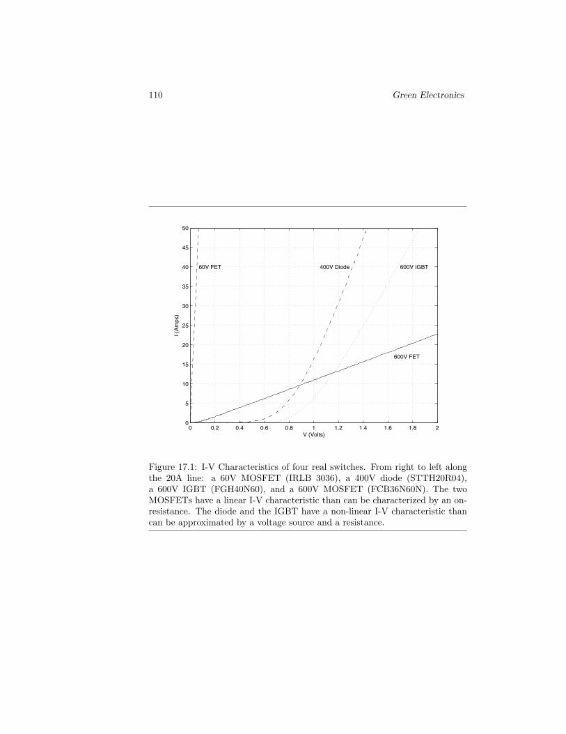
110 Green Electronics
0 0.2 0.4 0.6 0.8 1 1.2 1.4 1.6 1.8 20
5
10
15
20
25
30
35
40
45
50
V (Volts)
I (Am
ps)
60V FET
600V FET
400V Diode 600V IGBT
Figure 17.1: I-V Characteristics of four real switches. From right to left alongthe 20A line: a 60V MOSFET (IRLB 3036), a 400V diode (STTH20R04),a 600V IGBT (FGH40N60), and a 600V MOSFET (FCB36N60N). The twoMOSFETs have a linear I-V characteristic than can be characterized by an on-resistance. The diode and the IGBT have a non-linear I-V characteristic thancan be approximated by a voltage source and a resistance.

Copyright (c) 2011-14 by W.J Dally, all rights reserved 111
the I-V curve with two lines. The IGBT in Figure 17.1 for example can bemodeled as an 0.9V source in series with a 20mΩ resistor. The low incrementalresistance of IGBTs relative to MOSFETs make them attractive for high-voltage— above about 400V — applications. At 600V for example, our example IGBThas lower drop — and hence lower conduction losses for currents above 13A.
The fixed diode drop of an IGBT or diode make them inappropraite for useat very low-voltages where such a drop would cause excessive losses. Dropping0.9V in a 1V power supply would result in 47% loss. Even in a 10V supplythe 8% loss would be considered unacceptable. Such supplies use synchronousrectification to replace diodes with MOSFETs that have a much lower voltagedrop.
17.2 AC Characteristics of FETs and IGBTs
While Figure 17.1 shows the static characteristics of real switches Figure 17.2shows the dynamic characteristics. This figure shows the non-zero switchingtime of these real devices and its effect on switching losses.
The top panel of this figure shows a 600V MOSFET switching 20A through500V in the boost configuration shown in Figure 17.3. At the start of time theMOSFET is off. At 10ns the gate of the MOSFET is driven to 15V with a 30nsrise time and a 2.2-Ohm gate-drive resistor. When the rising gate reaches thethreshold voltage VT of the MOSFET, it turns on very quickly with the currentrising to 20A in about 1ns. The voltage then falls through 500V over about10ns — limited by the parasitic drain capacitance of the FET.
The bottom panel shows the power dissipation of the MOSFET — the prod-uct of voltage across the device with current through the device. At the pointwhere the current reaches 20A but the voltage is still 500V the FET is dissipat-ing 10kW. Fortunately this enormous power dissipation lasts only a brief periodof time and the total energy of this switching event is just 50µJ.
When the MOSFET turns off (starting at 160µs) the voltage rises to 500Vover about 10ns. Only when the voltage reaches 500V can the diode in theboost converter start conducting causing the current to abruptly fall to zero.The bottom panel shows the power dissipated during this transient. The totalturn-off switching energy is 52µJ.
The total switching loss over one cycle of operation for the boost converteris 102µJ — the sum of the 50µJ turn-on energy and the 52µJ turn-off energy.If this converter were running at 100kHz, the switching loss would be Psw =fEsw = 10.2W.
The waveforms and numbers in Figure 17.2 are unusually optimistic becausewe are neglecting parasitic inductance in the circuit which slows the currenttransient and also be cause we are assuming an ideal diode. Most real diodeshave reverse recovery characteristics, or at least substantial capacitance, thatcauses the current to overshoot for a considerable period before the voltagestarts to fall.
The middle panel of Figure 17.2 shows the AC characteristics of an IGBT
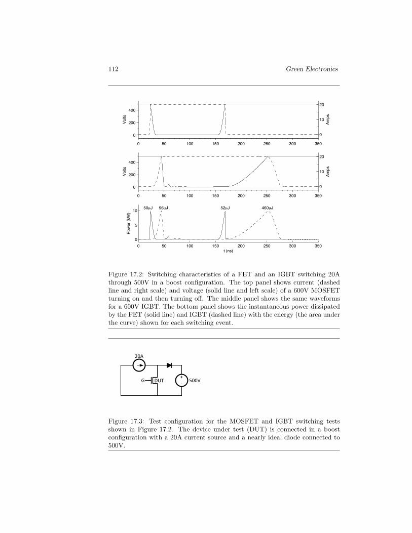
112 Green Electronics
0 50 100 150 200 250 300 350
0
200
400
Volts
0 50 100 150 200 250 300 350
0
200
400
Volts
0 50 100 150 200 250 300 3500
5
10
Pow
er (k
W)
t (ns)
50µJ 96µJ 52µJ 460µJ
0
10
20
Amps
0
10
20
Amps
Figure 17.2: Switching characteristics of a FET and an IGBT switching 20Athrough 500V in a boost configuration. The top panel shows current (dashedline and right scale) and voltage (solid line and left scale) of a 600V MOSFETturning on and then turning off. The middle panel shows the same waveformsfor a 600V IGBT. The bottom panel shows the instantaneous power dissipatedby the FET (solid line) and IGBT (dashed line) with the energy (the area underthe curve) shown for each switching event.
DUTG 500V
+
-
20A
Figure 17.3: Test configuration for the MOSFET and IGBT switching testsshown in Figure 17.2. The device under test (DUT) is connected in a boostconfiguration with a 20A current source and a nearly ideal diode connected to500V.

Copyright (c) 2011-14 by W.J Dally, all rights reserved 113
we see that the IGBT is slower than the FET for both turn-on and turn-off.Its turn-on time is about twice that of the FET — hence its turn-on switchingloss of 96µJ is about double the FET’s turn-on loss. The real issue with IGBTsis their turn-off time. The IGBT turn off time is an order of magnitude longerthan that of the FET and its 460µJ turn-off loss is correspondingly higher.
Slow turn off is characteristic of bipolar transistors in saturation. The powerhandling part of an IGBT is a bipolar transistor and time is required to clearthe minority carriers from the collector before it will turn off. IGBTs come invarious speed grades that trade voltage drop against turn off time. For slowswitching applications IGBTs are constructed with very low forward voltagedrop — by allowing the bipolar transistor to go deep into saturation. They payfor the low voltage drop with very long turn-off times - often more than 1µs.For higher-frequency applications IGBTs are constructed with a higher forwardvoltage drop to keep the bipolar transistor out of saturation and they switchconsiderably faster as a result.

114 Green Electronics

Chapter 18
Metal-Oxide Field EffectTransistors (MOSFETs)
Power MOSFETs are the workhorse switches for power electronic systems thatoperate at 200V or below. They switch on and off quickly and have a low,resistive, voltage drop when on. At voltages above 400V, IGBTs are usuallypreferred over MOSFETs because for a given cost they can handle more current.
To withstand high forward voltages when on, power MOSFETs are typicallyrealized using a vertical DMOS structure. Inherent in this structure is a bodydiode that conducts when the MOSFET is reverse biased. This makes theMOSFET a one-quadrant switch. It only controls current in the first quadrantof the V-I plane. It is always on in the third quadrant. If a four-quadrant switchis needed, two MOSFETs can be connected back-to-back.
The avalanche breakdown characteristic of the body diode acts to limit thereverse voltage across the MOSFET during transients. This device, for example,can absorb the energy stored in the leakage inductance in a simple flybackconverter (Figure 11.1). As long as the energy and power absorbed duringavalanche breakdown stay within limits the device can be used in this mannerwith no adverse effects.
18.1 Simple Model
Figure 18.1(a) shows the schematic symbol for a power MOSFET. The bodydiode is explicitly shown because it is an important circuit element. The MOS-FET has three terminals: gate, source, and drain. The gate is the controlterminal which controls current flow between the source and the drain. Un-like a planar MOSFET, the source and drain terminals are not symmetricaland cannot be interchanged. The source terminal of the MOSFET is internallyconnected to the body terminal of MOSFET so we do not show this terminalseparately.
115

116 Green Electronics
Gate
Drain
Source
Drain
Source
GateRon
Dbody
(a) (b)
Figure 18.1: (a) Schematic symbol for a MOSFET with the body diode explicitlyshown. (b) Simple switch-resistor model for a MOSFET.
A simple model of the power MOSFET is shown in Figure 18.1(b). TheMOSFET behavior is modeled by a switch and a resistor. When the MOSFETis fully-on the source and drain are connected by a resistor with value Ron.When the MOSFET is off the source and drain are disconnected. The bodydiode has its own characteristics that we will visit in Chapter 19.
When the voltage between the gate and the source, VGS exceeds the thresholdvoltage of the device VT , the MOSFET is on. When VGS = Von the MOSFET isfully-on and has resistance Ron between the source and drain. When VGS < VT
the MOSFET is off.During the turn-on and turn-off transient we approximate the conductance
of the FET with a straight line. If the turn-on time is ton the conductance attime t < ton is approximately
G(t) =t
tonRon(18.1)
In Section 18.3 we see that this linear current ramp is due to the linear buildup of charge in the channel during turn on.
18.2 Structure
Figure 18.2 shows the physical structure of a typical power MOSFET. Thesource terminal is connected to both the P+ body region and the N+ drain
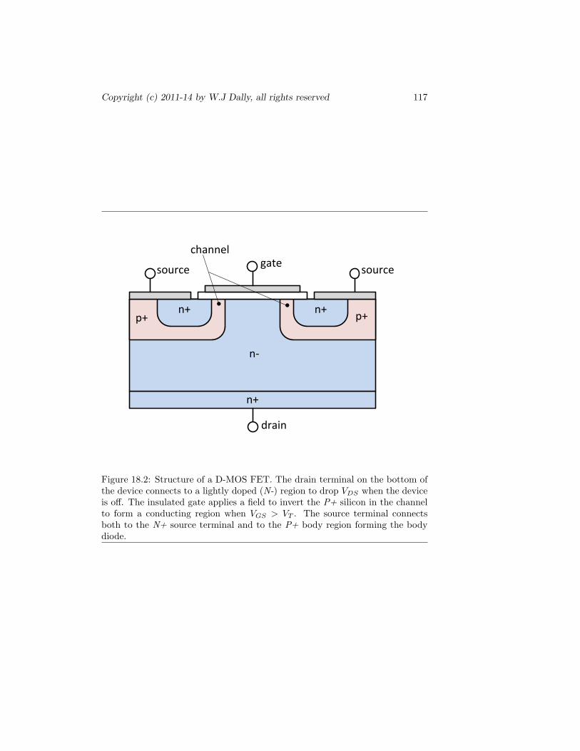
Copyright (c) 2011-14 by W.J Dally, all rights reserved 117
n+
p+n+
n-
p+n+
gatesource source
drain
channel
Figure 18.2: Structure of a D-MOS FET. The drain terminal on the bottom ofthe device connects to a lightly doped (N-) region to drop VDS when the deviceis off. The insulated gate applies a field to invert the P+ silicon in the channelto form a conducting region when VGS > VT . The source terminal connectsboth to the N+ source terminal and to the P+ body region forming the bodydiode.

118 Green Electronics
0 10 20 30 40 50 60 70 80 900
1
2
3
4
5
6
7
8
9
10
QG (nC)
V GS (V
)
Figure 18.3: Gate voltage (VGS) as a function of gate charge QG. This curveshows how the incremental capacitance (the inverse slope of the curve) changeswith voltage. The gate has a fixed capacitance (linear curve) until VGS = VT =5V. At this point the incremental capacitance becomes very large, VGS remainsnearly constant as charge is added, until the channel is fully inverted. The gatethen takes on a different fixed capacitance as VGS increases above VT .
terminal. The gate terminal applies a field to the channel, the portion of theP+ region under the gate. The drain terminal is connected to the far side ofthe vertical N- region.
When the gate is driven above the threshold voltage, the P+ region underthe gate becomes inverted, acting like an N region and resistively connectingthe source and drain N-regions. When the gate is low, the junction between theP+ body region and the N- drain region is reverse biased. The reverse voltageis dropped across a depletion region that forms mostly in the lightly-doped N-region. If too large a reverse voltage is applied, the depletion region will growcompletely across the channel connecting the source and drain and resulting inbreakdown.

Copyright (c) 2011-14 by W.J Dally, all rights reserved 119
18.3 Dynamics
The speed of a MOSFET is governed by the time required to transfer chargeto or from the channel via the gate terminal. The MOSFET can be turned on(and off) as quickly as charge can be moved in to (or out of) the channel. Oncethe channel inverts, all charge carriers transferred into the channel act to carrycharge from drain to source. Hence, the more charge in the channel, the morecarriers and the higher the conductance of the channel. When the gate terminalis fully on the channel is fully inverted and no further charge is transferred, atthis point the conductance of the channel is Gon = 1/Ron.
The speed of charge transfer, and hence of MOSFET switching, is governedboth by the internal resistance and inductance of the gate and source terminalsand by the characteristics of the gate-drive circuit that completes the circuitbetween gate and source. We describe gate-drive circuits in more detail inChapter 22.
The capacitance seen between a MOSFET’s gate and source terminals ishighly variable. For this reason MOSFET manufacturers specify a total gatecharge QG in addition to specifying CGS . The charge QG is more useful forunderstanding switching dynamics.
Figure 18.3 illustrates the variation in capacitance (the inverse slope of the V-Q curve) as a function of gate charge for a 600V 90mΩ MOSFET (FCB36N60N).As the gate charges from VGS = 0 to VT the capacitance is fixed. This is thecapacitance from the gate terminal to the source and drain terminals. WhenVGS reaches VT , at 15nC of charge the channel inverts and the incrementalcapacitance becomes very low. During this period the drain is rising and thecharge applied to the gate is consumed charging the Miller capacitance CDG.VGS holds nearly constant as the charge ramps from 15nC to 40nC. At this pointthe drain stops rising and the incremental capacitance becomes a different fixedvalue.
If the gate is being driven with a 1A current source Figure 18.3 shows thevoltage on the gate as a function of time. The current source deposits 1nC on thegate every 1ns. With this drive the transistor woudl remain off for the first 15ns.Then, when VGS = VT = 4.5V its conductance begins to linearly ramp from 0to 11S over the next 25ns, 0.44S/ns. If the MOSFET is in the configurationof Figure 17.2 with VDS = 500V, current ramps at (500)(0.44)=222A/ns. Inpractice finite inductance in the circuit slows the current ramp to somethingconsiderably slower.
18.4 Parasitic Elements
Because a properly driven MOSFET can turn on blindingly fast, the parasiticcircuit elements can have a first-order effect on the performance of the MOSFETand its switching losses. Figure 18.4 shows the major parasitic circuit elementsassociated with a typical MOSFET. Table 18.4 lists typical parasitic values fora 600V 100mΩ power MOSFET.
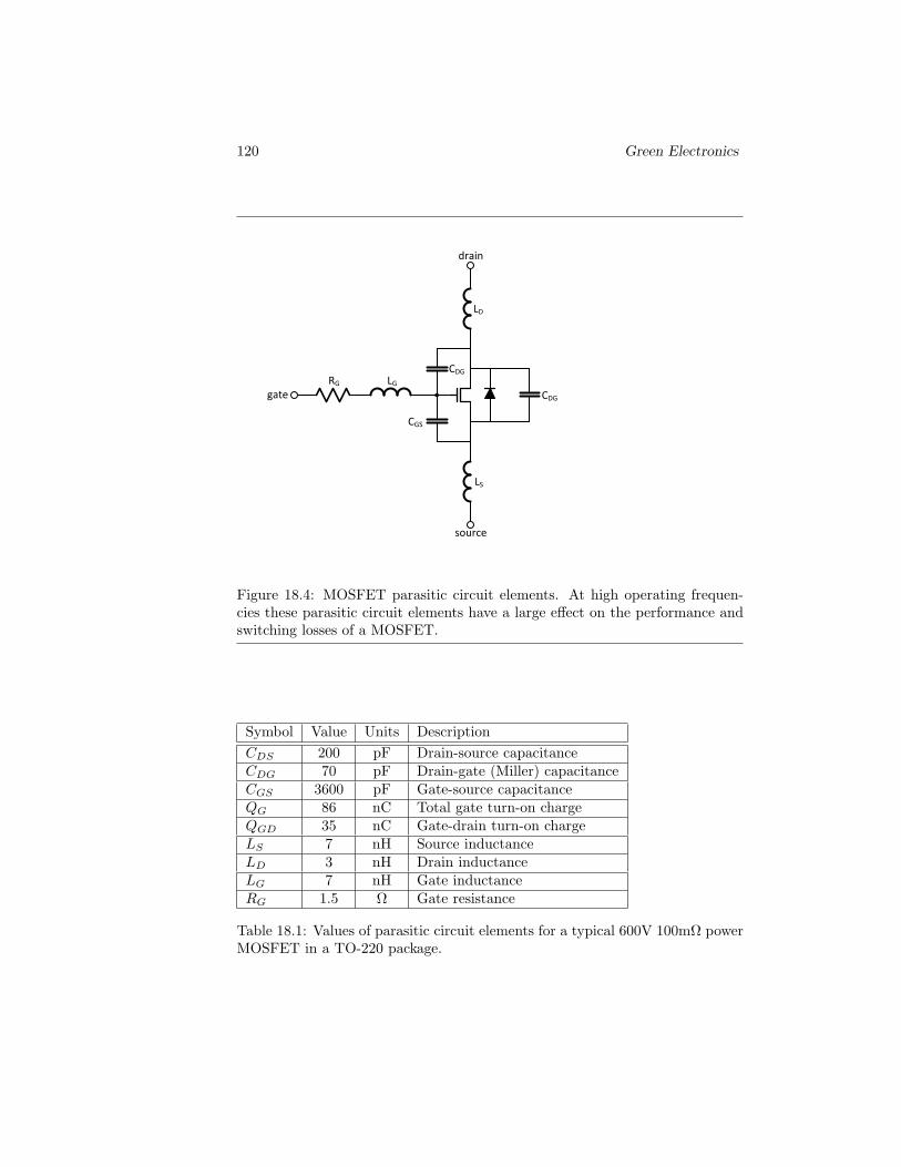
120 Green Electronics
CDG
LS
LGRG
LD
CDG
CGS
source
gate
drain
Figure 18.4: MOSFET parasitic circuit elements. At high operating frequen-cies these parasitic circuit elements have a large effect on the performance andswitching losses of a MOSFET.
Symbol Value Units DescriptionCDS 200 pF Drain-source capacitanceCDG 70 pF Drain-gate (Miller) capacitanceCGS 3600 pF Gate-source capacitanceQG 86 nC Total gate turn-on chargeQGD 35 nC Gate-drain turn-on chargeLS 7 nH Source inductanceLD 3 nH Drain inductanceLG 7 nH Gate inductanceRG 1.5 Ω Gate resistance
Table 18.1: Values of parasitic circuit elements for a typical 600V 100mΩ powerMOSFET in a TO-220 package.

Copyright (c) 2011-14 by W.J Dally, all rights reserved 121
Parasitic inductance, which is largely due to the package, limits how fastcurrent can ramp in the gate-source and source-drain circuits. While we listall three lead inductances, for circuit analysis we are concerned with two sums.The gate-source inductance LGS = LG +LS determines how fast the gate drivercan ramp current to charge the gate. Given LGS=14nH for our typical FET,a 10V gate driver can produce a current slope of at most 0.7A/ns. In practicethe gate driver and circuit board will add more inductance and some of the 10Vwill drop across the resistance of the FET and the gate driver so we may belucky to get 0.5A/ns.
The drain-source inductance LDS = LD+LS gets added to other inductancesin the loop supplying current during the switching transient to limit currentramp during turn-on and turn-off. Our typical FET has LDS = 10nH. Parasiticinductances in the diode, capacitor, and circuit board traces that complete theloop can easily triple this bringing the total loop inductance to Lloop =30nH.With 500V across 30nH the current slope is limited to 17A/ns. This is an orderof magnitude slower than the FET itself is capable of.
Energy stored in the loop inductance causes overshoot and ringing. Considerthe circuit of Figure 17.3 but with 30nH of inductance around the loop thatincludes the FET, diode, and voltage source. As the drain falls to groundduring turn-on, the current in the loop inductance will exceed 20A. The excesscurrent will ring out in an LRC circuit formed by Lloop, Ron, and CDS , and theenergy represented by this excess current will be lost. During turn-off 20A inLloop represents 12µJ of stored energy that will be lost and can lead the drainto overshoot.
Minimizing inductance is of first-order importance. Newer packages, such asthinPAK have LDS as low as 3nH which, in conjuction with careful board layoutand parallel arrays of bypass capacitors, greatly speeds switching and reduceslosses.
The Miller capacitance CDG is multiplied by the difference in drain vs gatevoltage swing. This has two ill effects. First, due to the Miller effect, CGD
accounts for over a third of the total gate charge slowing gate turn-on. ChargeQGD is CDG multiplied by the 500V swing. More critical, however, is that thiscapacitive feedback can lead to oscillations. During turn-on with a slow gatedriver capacitive feedback can turn the FET back off. This in turn causes thedrain to rise turning the FET back on, and so on. A similar phenomena canoccur during turn-off where the rising drain turns the FET back on. In eithercase the resulting oscillations can greatly increase switching losses.
The drain-source capacitance CDS along with the capacitance of the diodemust be charged and discharged as the drain rises and falls. This both leads toCV 2 energy losses and increases switching losses by slowing the drain transition.At 500V, the energy stored on 200pF is 50µJ.
The gate-source capacitance is not really a parasitic element since its criticalto the operation of the FET. However this large capacitance complicates thedesign of the gate drive circuit. Because the capacitance varies with voltage, asexplained in Section 18.3, it is more useful to design the gate driver to providethe charge QG than to drive CGS .

122 Green Electronics
18.5 Avalanche Energy
Inductor current flowing into the drain node of a MOSFET as it turns off cancharge the drain node above VDSmax. This occurs, for example, in a flybackconverter (Figure 11.3) where the energy from the leakage inductance of thetransformer is transferred to the drain node. When VDS rises above VDSmax thereverse-biased body diode of the MOSFET is driven into avalanche breakdownand begins to conduct.
This avalanche breakdown is not destructive to the MOSFET as long as thetotal energy of the event is within limits. The FCN36N60 FET, for example,can handle up to 1.8J of energy in a single avalanche breakdown event andup to 3.12mJ in repetitive events. This avalanche breakdown serves a usefulpurpose in applications such as the flyback converter where it serves as theenergy-absorbing device in Figure 11.3.
18.6 Typical MOSFETs
The key data-sheet parameters of six representative MOSFETs are shown inTable 18.2. The first four columns are silicon MOSFETs with voltage ratings of20V, 60V, 200V, and 600V respectively. They illustrate how key MOSFET pa-rameters vary with voltage. The fifth column is a 200V gallium-nitride (GAN)FET. It is instructive to compare the properties of the 200V GAN FET withthe 200V Si FET. The final column is a 1200V silicon-carbide (SiC) FET. Com-paring this device to the 600V silicon FET highlights its properties.
The first row, VDSMax is the maximum drain-source voltage supported bythe FET. The second row
describe the partswalk through the parameters
18.7 Exercises

Copyright (c) 2011-14 by W.J Dally, all rights reserved 123
Dev
ice
20V
IRLB
3036
FC
B36
N60
NE
PC
2010
C2M
0025
120
Uni
tsD
escr
ipti
onV
DSm
ax
2060
200
600
200
1200
VM
axim
umV
DS
Ron
1.9
8118
25m
ΩO
nre
sist
ance
QG
9186
516
1nC
Gat
ech
arge
CO
SS
1020
8027
022
0pF
Out
put
capa
cita
nceC
SD
+C
GD
I Dm
ax
195
3612
90A
Max
imum
cont
inuo
usdr
ain
curr
ent
I DM
1100
108
6025
0A
Max
imum
puls
eddr
ain
curr
ent
EA
S29
018
00m
JSi
ngle
-eve
ntav
alan
che
ener
gyP
max
380
312
463
WM
axim
umpo
wer
diss
ipat
ion
V2/R
1.9
4.4
2.2
58M
WFig
ure
ofm
erit
V2/RQ
G21
5244
036
0m
V/s
Fig
ure
ofm
erit
Tab
le18
.2:
Key
para
met
ers
ofsi
xfie
ld-e
ffect
tran
sist
ors.

124 Green Electronics
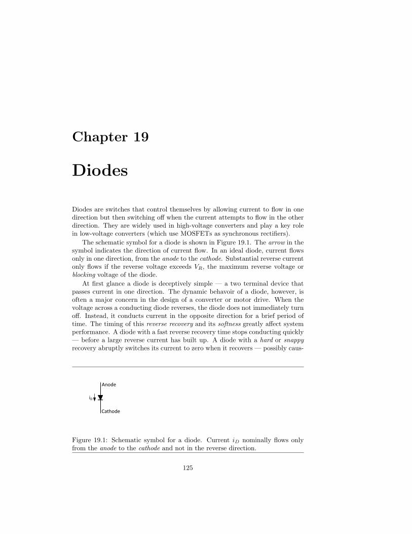
Chapter 19
Diodes
Diodes are switches that control themselves by allowing current to flow in onedirection but then switching off when the current attempts to flow in the otherdirection. They are widely used in high-voltage converters and play a key rolein low-voltage converters (which use MOSFETs as synchronous rectifiers).
The schematic symbol for a diode is shown in Figure 19.1. The arrow in thesymbol indicates the direction of current flow. In an ideal diode, current flowsonly in one direction, from the anode to the cathode. Substantial reverse currentonly flows if the reverse voltage exceeds VR, the maximum reverse voltage orblocking voltage of the diode.
At first glance a diode is deceptively simple — a two terminal device thatpasses current in one direction. The dynamic behavoir of a diode, however, isoften a major concern in the design of a converter or motor drive. When thevoltage across a conducting diode reverses, the diode does not immediately turnoff. Instead, it conducts current in the opposite direction for a brief period oftime. The timing of this reverse recovery and its softness greatly affect systemperformance. A diode with a fast reverse recovery time stops conducting quickly— before a large reverse current has built up. A diode with a hard or snappyrecovery abruptly switches its current to zero when it recovers — possibly caus-
Anode
Cathode
iD
Figure 19.1: Schematic symbol for a diode. Current iD nominally flows onlyfrom the anode to the cathode and not in the reverse direction.
125

126 Green Electronics
iD
RS
Gmin CDvD
Figure 19.2: Simple DC model for a diode consists of a current source iD, aseries resistance RS , and a parallel conductance, Gmin.
ing damaging voltage transients across stray inductances. A diode with a softrecovery, on the other hand, more gradually reduces its reverse current to zero— reducing inductive voltage transients. Some diodes are also slow to turn on.This forward recovery behavior can also cause issues.
19.1 Simple Model
A simple large-signal model for a diode operated above its maximum reversevoltage ,show in Figure 19.2, consists of a dependent current source, two re-sistances, and a variable capacitance. The series resistance RS dominates thevoltage drop of the diode at high currents. The parallel conductance Gmin de-termines the current when reverse biased and at low positive voltages. It isincluded primarily to aid convergence of simulations. The DC diode current iDdepends exponentially on the voltage across the current source vD:
iD = IS
(exp
(vD
NVT
)− 1)
(19.1)
Where VT is the thermal voltage which is given by:
VT =KT
q(19.2)
At room temperature (300 K), VT = 25.85mV. Thus each time the diodevoltage increases by 28.85N mV, current increases by a factor of e. Because VT
increases linearly with temperature, one might think that diode current woulddecrease as temperature increases. This is not the case because the saturation

Copyright (c) 2011-14 by W.J Dally, all rights reserved 127
0 0.2 0.4 0.6 0.8 1 1.2 1.4 1.6 1.8 20
5
10
15
20
25
V (Volts)
I (Am
ps)
STTH20R04
UF1007
UF1001
MBR40250
1N4004
Figure 19.3: I-V Characteristics of the diodes from Table 19.1. These curvesillustrate how one sacrifices low VF for fast switching time or high VR.
current IS has a stronger temperature dependence.
IS = I0
(T
T0
)X/N
(19.3)
(19.4)
Where T is the diode temperature (in K), T0 is not nominal temperature(typically 300 K), I0 is the saturation current at T0, N is the ideality parameterof the diode, and X is a parameter of the diode in question. For typical siliconjunction diodes X = 3 and for Schottky diodes, X = 2.
Curves showing the first quadrant of this DC I-V relationship for severaltypical diodes are show in Figure 19.3. As voltage is increased, the currentincreases exponentially until the voltage drop across the series resistance exceedsthe voltage drop across the current source. At currents above this point, theV-I characteristic is dominated by the series resistance RS . The slope of thisportion of the curve is 1/RS .
The V-I curve of the 1N4004 diode, plotted in Figure 19.3 are derived fromparameters IS = 3.70nA, N = 1.774 and RS = 17.56mΩ .
The diode capacitance CD in Figure 19.2 dominates the transient response

128 Green Electronics
of the diode. It is the sum of junction capacitance and the diffusion capacitance:
CD = Cj + Cd (19.5)
Where the junction capacitance dominates at zero and reverse bias and decreaseswith increasing reverse bias:
Cj =Cj0√1− V
V0
(19.6)
The diffusion capacitance dominates during forward bias and accounts for mi-nority carriers stored in the diode:
Cd =τTNVT
iD (19.7)
Where τT is the transit time of the diode. The diffusion capacitance accountsfor the reverse recovery time of the diode.
19.2 Key Parameters
Diodes come in many different varieties. In this book we are concerned onlywith power diodes, sometimes referred to as rectifiers, not small signal diodes,RF diodes, varactors, or other sundry types. Even power diodes come in manyflavors depending on the voltage, current, and speed required.
The key data-sheet parameters of some representative power diodes areshown in Table 19.1. The I-V characteristics of these diodes are plotted inFigure 19.3. The first diode, a STTH20R04 is the diode shown in Figure 17.1.This is a 400V, 20A diode. That is, it will block 400V across the diode in thereverse direction and will carry an average forward current of 20A when biasedin the forward direction. Forward current specifications need to be read care-fully. This 20A diode can handle non-repetitive surge current of up to 150Aand RMS forward current up to 50A. The STTH20R04 is specified as havinga forward voltage of VF = 1.5V at 25C and 20A. This is a rather pessimisticmaximum. Figure 19.3 shows the diode dropping 1.05V under these conditions.This voltage drop is reduced by 0.35V at 125C which leads to current hoggingas described in Section 19.5 below.
The STTH20R04 is a fast diode — with a reverse recovery time of 35ns —and has a moderately soft recovery with S = 0.3. (The softness factor will beexplained in more detail in Section 19.3 below.)
The second diode in the table is a 1N4004. This is a slow, 1A, 400V diodeoften used to rectify 60Hz AC. The 1N4004 is rated for average forward currentIF =1A, as are the next two diodes in the table. However, all three of these 1Adiodes can handle non-repetitive surge currents of up to IFSM=30A.

Copyright (c) 2011-14 by W.J Dally, all rights reserved 129
Dev
ice
STT
H20
R04
1N40
04U
F10
01U
F10
07M
BR
4025
0U
nits
Des
crip
tion
VR
400
400
5010
0025
0V
olts
Max
imum
reve
rse
volt
age
I F20
11
140
Am
psM
axim
umfo
rwar
dcu
rren
tI F
SM
150
3030
3015
0A
mps
Max
imum
non-
repe
titi
vefo
rwar
dsu
rge
curr
ent
VF
1.5
11
1.7
0.86
Vol
tsFo
rwar
dvo
ltag
et r
r35
1000
5075
35ns
Rev
erse
reco
very
tim
eS
0.3
Soft
ness
fact
ort f
r15
0ns
Forw
ard
reco
very
tim
eV
FP
2.5
Vol
tsSo
ftne
ssfa
ctor
Tab
le19
.1:
Key
para
met
ers
offiv
edi
odes
.
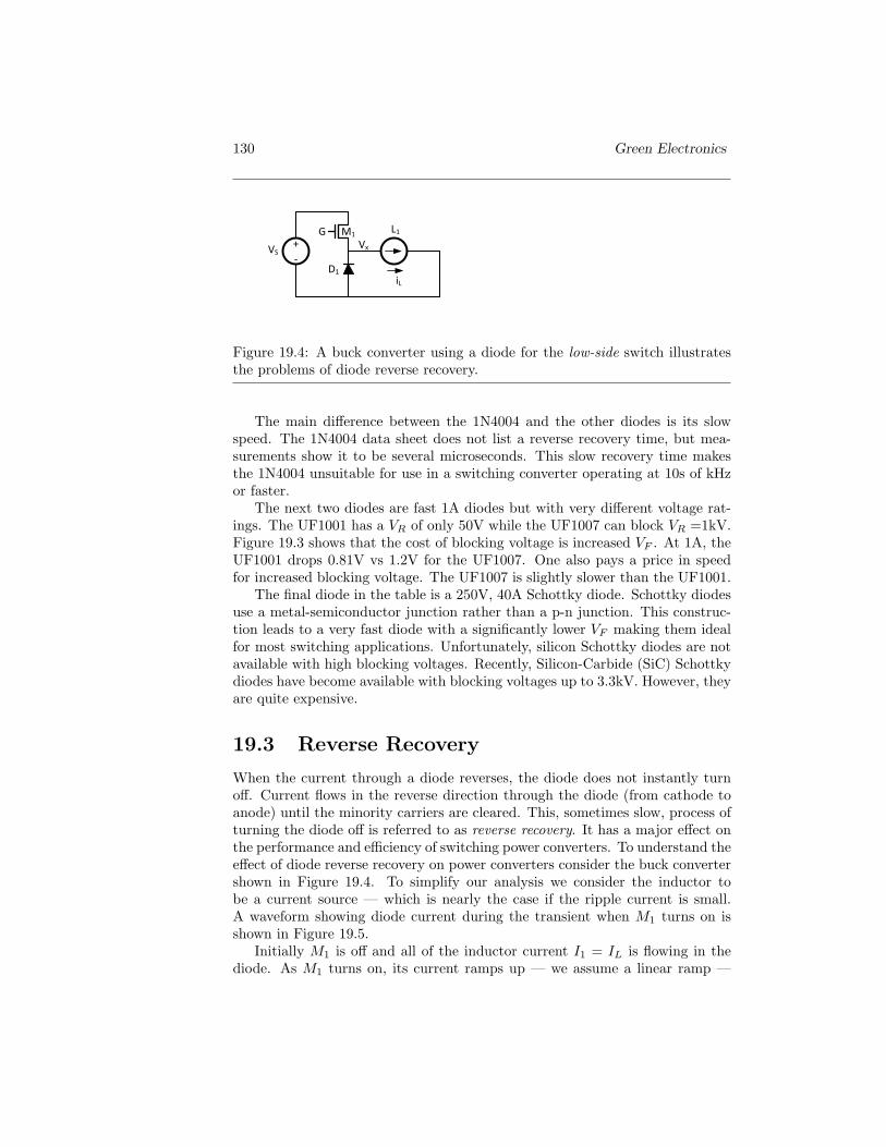
130 Green Electronics
L1
D1
G M1
Vx+
-VS
iL
Figure 19.4: A buck converter using a diode for the low-side switch illustratesthe problems of diode reverse recovery.
The main difference between the 1N4004 and the other diodes is its slowspeed. The 1N4004 data sheet does not list a reverse recovery time, but mea-surements show it to be several microseconds. This slow recovery time makesthe 1N4004 unsuitable for use in a switching converter operating at 10s of kHzor faster.
The next two diodes are fast 1A diodes but with very different voltage rat-ings. The UF1001 has a VR of only 50V while the UF1007 can block VR =1kV.Figure 19.3 shows that the cost of blocking voltage is increased VF . At 1A, theUF1001 drops 0.81V vs 1.2V for the UF1007. One also pays a price in speedfor increased blocking voltage. The UF1007 is slightly slower than the UF1001.
The final diode in the table is a 250V, 40A Schottky diode. Schottky diodesuse a metal-semiconductor junction rather than a p-n junction. This construc-tion leads to a very fast diode with a significantly lower VF making them idealfor most switching applications. Unfortunately, silicon Schottky diodes are notavailable with high blocking voltages. Recently, Silicon-Carbide (SiC) Schottkydiodes have become available with blocking voltages up to 3.3kV. However, theyare quite expensive.
19.3 Reverse Recovery
When the current through a diode reverses, the diode does not instantly turnoff. Current flows in the reverse direction through the diode (from cathode toanode) until the minority carriers are cleared. This, sometimes slow, process ofturning the diode off is referred to as reverse recovery. It has a major effect onthe performance and efficiency of switching power converters. To understand theeffect of diode reverse recovery on power converters consider the buck convertershown in Figure 19.4. To simplify our analysis we consider the inductor tobe a current source — which is nearly the case if the ripple current is small.A waveform showing diode current during the transient when M1 turns on isshown in Figure 19.5.
Initially M1 is off and all of the inductor current I1 = IL is flowing in thediode. As M1 turns on, its current ramps up — we assume a linear ramp —
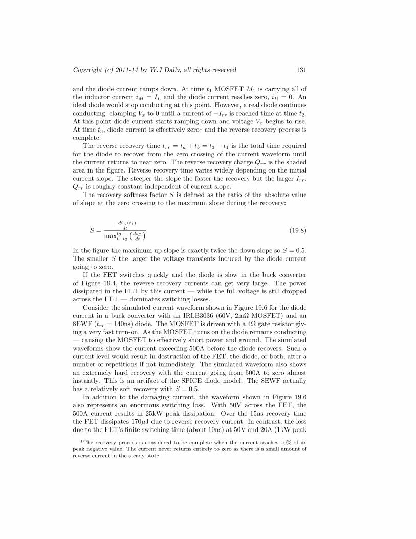
Copyright (c) 2011-14 by W.J Dally, all rights reserved 131
and the diode current ramps down. At time t1 MOSFET M1 is carrying all ofthe inductor current iM = IL and the diode current reaches zero, iD = 0. Anideal diode would stop conducting at this point. However, a real diode continuesconducting, clamping Vx to 0 until a current of −Irr is reached time at time t2.At this point diode current starts ramping down and voltage Vx begins to rise.At time t3, diode current is effectively zero1 and the reverse recovery process iscomplete.
The reverse recovery time trr = ta + tb = t3 − t1 is the total time requiredfor the diode to recover from the zero crossing of the current waveform untilthe current returns to near zero. The reverse recovery charge Qrr is the shadedarea in the figure. Reverse recovery time varies widely depending on the initialcurrent slope. The steeper the slope the faster the recovery but the larger Irr.Qrr is roughly constant independent of current slope.
The recovery softness factor S is defined as the ratio of the absolute valueof slope at the zero crossing to the maximum slope during the recovery:
S =−diD(t1)
dt
maxt3t=t2
(diD
dt
) (19.8)
In the figure the maximum up-slope is exactly twice the down slope so S = 0.5.The smaller S the larger the voltage transients induced by the diode currentgoing to zero.
If the FET switches quickly and the diode is slow in the buck converterof Figure 19.4, the reverse recovery currents can get very large. The powerdissipated in the FET by this current — while the full voltage is still droppedacross the FET — dominates switching losses.
Consider the simulated current waveform shown in Figure 19.6 for the diodecurrent in a buck converter with an IRLB3036 (60V, 2mΩ MOSFET) and an8EWF (trr = 140ns) diode. The MOSFET is driven with a 4Ω gate resistor giv-ing a very fast turn-on. As the MOSFET turns on the diode remains conducting— causing the MOSFET to effectively short power and ground. The simulatedwaveforms show the current exceeding 500A before the diode recovers. Such acurrent level would result in destruction of the FET, the diode, or both, after anumber of repetitions if not immediately. The simulated waveform also showsan extremely hard recovery with the current going from 500A to zero almostinstantly. This is an artifact of the SPICE diode model. The 8EWF actuallyhas a relatively soft recovery with S = 0.5.
In addition to the damaging current, the waveform shown in Figure 19.6also represents an enormous switching loss. With 50V across the FET, the500A current results in 25kW peak dissipation. Over the 15ns recovery timethe FET dissipates 170µJ due to reverse recovery current. In contrast, the lossdue to the FET’s finite switching time (about 10ns) at 50V and 20A (1kW peak
1The recovery process is considered to be complete when the current reaches 10% of itspeak negative value. The current never returns entirely to zero as there is a small amount ofreverse current in the steady state.
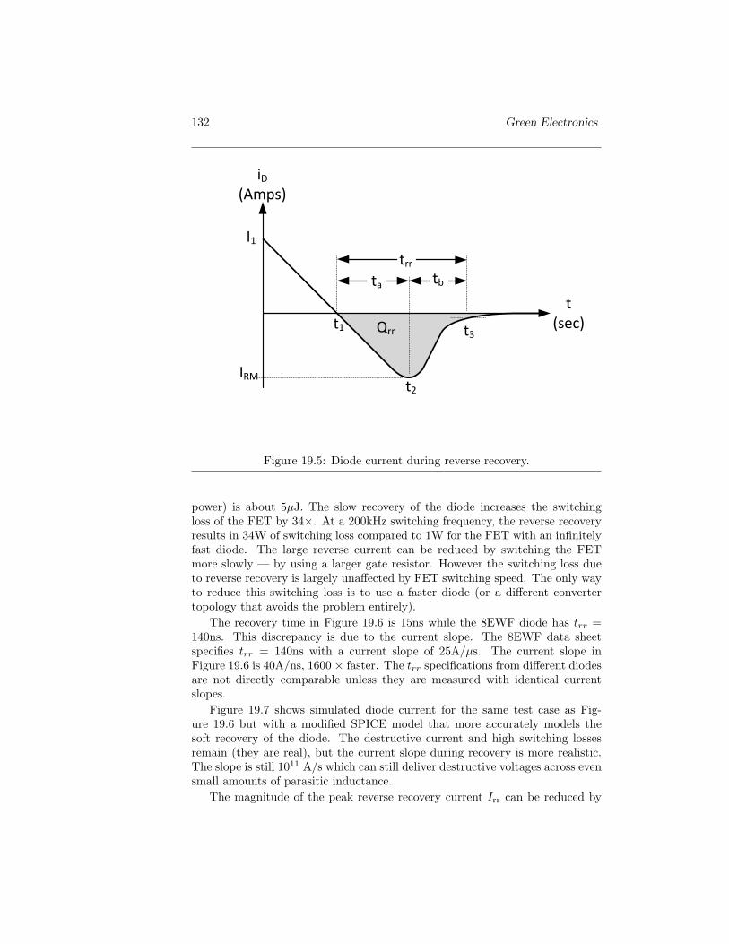
132 Green Electronics
I1
IRM
ta tb
trr
Qrr
iD
(Amps)
t(sec)t1
t2
t3
Figure 19.5: Diode current during reverse recovery.
power) is about 5µJ. The slow recovery of the diode increases the switchingloss of the FET by 34×. At a 200kHz switching frequency, the reverse recoveryresults in 34W of switching loss compared to 1W for the FET with an infinitelyfast diode. The large reverse current can be reduced by switching the FETmore slowly — by using a larger gate resistor. However the switching loss dueto reverse recovery is largely unaffected by FET switching speed. The only wayto reduce this switching loss is to use a faster diode (or a different convertertopology that avoids the problem entirely).
The recovery time in Figure 19.6 is 15ns while the 8EWF diode has trr =140ns. This discrepancy is due to the current slope. The 8EWF data sheetspecifies trr = 140ns with a current slope of 25A/µs. The current slope inFigure 19.6 is 40A/ns, 1600 × faster. The trr specifications from different diodesare not directly comparable unless they are measured with identical currentslopes.
Figure 19.7 shows simulated diode current for the same test case as Fig-ure 19.6 but with a modified SPICE model that more accurately models thesoft recovery of the diode. The destructive current and high switching lossesremain (they are real), but the current slope during recovery is more realistic.The slope is still 1011 A/s which can still deliver destructive voltages across evensmall amounts of parasitic inductance.
The magnitude of the peak reverse recovery current Irr can be reduced by

Copyright (c) 2011-14 by W.J Dally, all rights reserved 133
0 5 10 15 20 25 30−600
−500
−400
−300
−200
−100
0
100
t (ns)
i D (A
mps
)
Figure 19.6: Simulation of diode current during reverse recovery for an 8EWFdiode (trr =140ns).
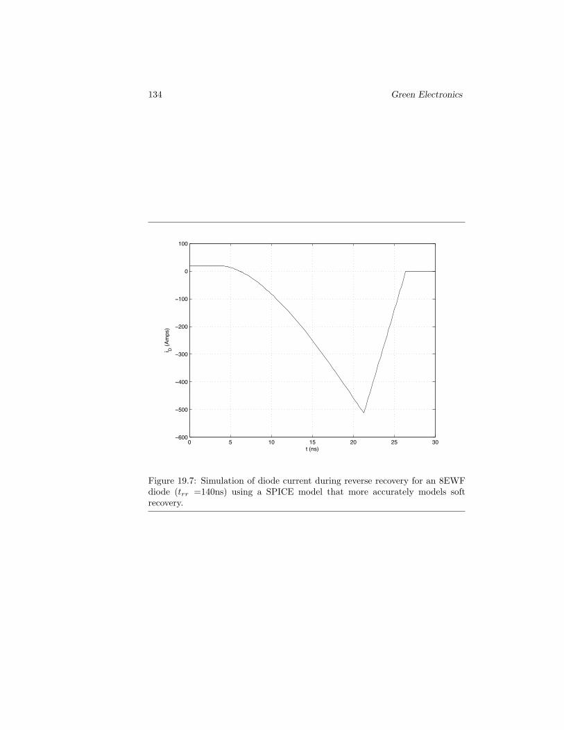
134 Green Electronics
0 5 10 15 20 25 30−600
−500
−400
−300
−200
−100
0
100
t (ns)
i D (A
mps
)
Figure 19.7: Simulation of diode current during reverse recovery for an 8EWFdiode (trr =140ns) using a SPICE model that more accurately models softrecovery.
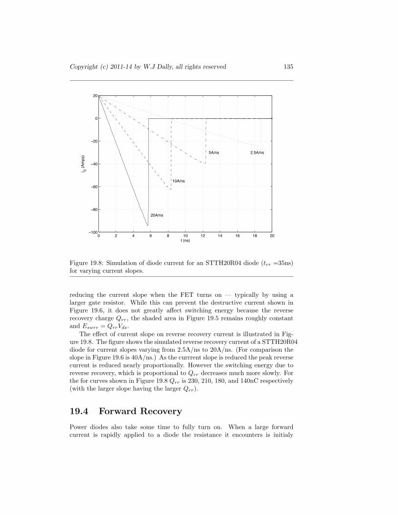
Copyright (c) 2011-14 by W.J Dally, all rights reserved 135
0 2 4 6 8 10 12 14 16 18 20−100
−80
−60
−40
−20
0
20
t (ns)
i D (A
mps
)
20A/ns
10A/ns
5A/ns 2.5A/ns
Figure 19.8: Simulation of diode current for an STTH20R04 diode (trr =35ns)for varying current slopes.
reducing the current slope when the FET turns on — typically by using alarger gate resistor. While this can prevent the destructive current shown inFigure 19.6, it does not greatly affect switching energy because the reverserecovery charge Qrr, the shaded area in Figure 19.5 remains roughly constantand Eswrr = QrrVds.
The effect of current slope on reverse recovery current is illustrated in Fig-ure 19.8. The figure shows the simulated reverse recovery current of a STTH20R04diode for current slopes varying from 2.5A/ns to 20A/ns. (For comparison theslope in Figure 19.6 is 40A/ns.) As the currrent slope is reduced the peak reversecurrent is reduced nearly proportionally. However the switching energy due toreverse recovery, which is proportional to Qrr decreases much more slowly. Forthe for curves shown in Figure 19.8 Qrr is 230, 210, 180, and 140nC respectively(with the larger slope having the larger Qrr).
19.4 Forward Recovery
Power diodes also take some time to fully turn on. When a large forwardcurrent is rapidly applied to a diode the resistance it encounters is initialy
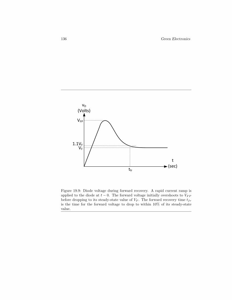
136 Green Electronics
VFP
VF
tfr
vD
(Volts)
t(sec)
1.1VF
Figure 19.9: Diode voltage during forward recovery. A rapid current ramp isapplied to the diode at t − 0. The forward voltage initially overshoots to VFP
before dropping to its steady-state value of VF . The forward recovery time tfr
is the time for the forward voltage to drop to within 10% of its steady-statevalue.
Copyright (c) 2011-14 by W.J Dally, all rights reserved 137
higher, sometimes substantially higher, than the steady-state DC resistance.This is because the intrinsic region of the PIN diode initially has few chargecarriers. This high initial resistance can result in a high initial forward voltageVFP as shown in Figure 19.9. Once the density of charge carriers reaches itssteady-state value, the resistance of the diode drops to its steady-state vaue asdoes the forward voltage.
The STTH20R04 diode specifies a forward recovery time of tfr = 150nsand a maximum peak forward voltage of VFP = 2.5V (typical VFP is 1.7V).Compared to the steady state VF = 1.5V, this represents a worst-case initial67% increase in forward voltage.
Consider the buck converter of Figure 19.4. When transistor M1 turns off,iL is applied to diode D1 with a ramp that depends on the turn-off time ofM1 — which may be 10ns or less. Normally we would expect D1 to keep Vx
clamped to within VF of ground. However, during reverse recovery Vx may dropas low as VFP below ground. Depending on the circuitry attached to this node,a large negative undershoot could present a problem. Some diodes have a VFP
far worse than the 2.5V of the STTH20R04.
19.5 Current Hogging
Connecting multiple diodes in parallel — to handle a larger current can be prob-lematic because diode current increases with temperature. Unless the thermaldesign keeps the parallel diodes at nearly the same temperature or ballast resis-tors are placed in series with the diodes one diode may wind up hogging mostof the current — until it fails catastrophically.
This current hogging is an example of positive feedback. One diode gets alittle warmer than the others. This causes its current to increase. This in turncauses it to dissipate more power and get even warmer. The cycle continuesuntil the diode is very hot and carrying nearly all of the current.
Figure 19.10 shows the temperature sensitivity of a 1N4004 diode. As tem-perature increases the diode current at a given voltage increases significantly(or conversely the voltage at a given current decreases signficantly). Neglectingseries resistance, for a typical diode, current is proportional to a power of tem-perature (in K) as given by (19.1). At the rated current of 1A, increasing thetemperature by 1C decreases the voltage drop by approximately 1mV.
Referring to Figure 19.10, consider a case where four 1N4004 diodes areconnected in parallel to carry an average current of 4A. If one diode becomeshot (125C) while the others remain at room temperature (25C), the hot diodewill carry 3A of current while the cool diodes carry about 0.3A each. This willcause the hot diode to get hotter, causing it to carry even more current until itfails.
The dynamics of diode thermal runaway are illustrated in Figure 19.11. Thefigures shows simulated temperature (top panel) and current (bottom panel)for four diodes connected in parallel sharing a 20A load. One diode has athermal resistance to ambient that is 10% higher than the other three. This

138 Green Electronics
0.6 0.65 0.7 0.75 0.8 0.85 0.9 0.95 1 1.05 1.10
0.5
1
1.5
2
2.5
3
3.5
4
4.5
5
25°C
75°C
125°C
VD (Volts)
i D (A
mps
)
Figure 19.10: I-V characteristics of a 1N4004 diode at 25C, 75C, and 125C.Current increases as temperature increases leading to current hogging if multiplediodes are connected in parallel.

Copyright (c) 2011-14 by W.J Dally, all rights reserved 139
0 10 20 30 40 50 60 70 80 90 10050
100
150
200
250
Tem
p (°C
)
0 10 20 30 40 50 60 70 80 90 1000
2
4
6
8
10
i D (A
mps
)
t (ms)
Figure 19.11: Thermal runaway caused by current hogging with four diodesconnected in parallel carrying 20A and with a nominal thermal resistance of20C/W and a thermal time constant of 1ms. One diode has a thermal resistancethat is 10% higher than the others. The top panel shows diode temperatures.Diode current is shown in the bottom panel.
10% mismatch in thermal resistance leads to a 270% mismatch in current. Inthe steady state the hot diode (solid line) is carrying 9.5A of current while theother three diodes (dotted line) carry 3.5A each.
Thermal mismatches are quite common and can be significantly larger than10%. They may be caused by component placement, proximity to other powerdissipating components, the direction of convective or conductive heat flow, andother factors.
If diodes are to be placed in parallel, the thermal design should use a physicalarrangement that keeps the diode’s junction temperatures (not case tempera-tures) closely matched, and/or a ballast resistor should be placed in series witheach diode as shown in Figure 19.12 to reduce the current mismatch that resultsfrom temperature mismatch.
Figure 19.13 shows the effect of ballast resistors on the V-I characteristicsof a typical diode as a function of temperature. The figure shows the V-Icharacteristics for a 1N4004 diode with and without a 0.5Ω ballast resistor at25C and 125C. Without the ballast resistor, two diodes at the same voltage

140 Green Electronics
D1
R1
D2
R2
D3
R3
D4
R4
iT
Figure 19.12: To balance current through parallel diodes, a ballast resistorshould be inserted in series with each diode.
0 0.2 0.4 0.6 0.8 1 1.2 1.4 1.6 1.8 20
0.5
1
1.5
2
2.5
125°C No Ballast
25°C No Ballast
125°C Ballast
25°C Ballast
VD (Volts)
i D (A
mps
)
Figure 19.13: I-V Curves of 1N4004 diodes at 25C and 125∗C with and with-out 0.5Ω ballast resistors.

Copyright (c) 2011-14 by W.J Dally, all rights reserved 141
but different temperatures can have vastly different currents. At vD=0.8V, forexample, the 125C diode is carrying 0.9A while the 25C diode carries only0.1A.
Adding the ballast resistor greatly reduces this imbalance. At 1.1V for ex-ample the hot diode carries 0.6A while the current in the cool diode is 0.48A.The difference is narrowed from 0.8A to 0.12A. With ballast, the current dif-ference between the hot diode and the cold diode narrows further as currentincreases — the lines converge and at some current will cross over. This is be-cause resistors have a positive temperature coefficient — resistance increases,and hence current decreases, as temperature increases — naturally balancingcurrent between parallel resistors.
The downside of providing current balance using ballast resistors is the powerdissipated in the ballast resistors and their cost. In some cases the ballast resis-tor can be implemented with a foil trace on a printed-circuit board minimizingcost.
19.6 SPICE Models
The standard Berkeley SPICE diode model which is used in most derivatives ofthe SPICE circuit simulator can reasonably accurately capture the DC charac-teristics of a diode. However, it does a very poor job modeling the dynamicsof a diode — reverse recovery and forward recovery — that are important inpower electronics.
Even for the aspects of a diode that can be captured by the standard SPICEdiode model, accurate simulation depends on having an accurate model. Evenmodels from the diode manufacturers are not always accurate or may not beaccurate under the test conditions (e.g., current slope) important in your appli-cation. For any critical diode application there is no substitute for a physicalexperiment to measure the important parameters on a real diode.
The DC characteristics of a simulated diode are determined by SPICE pa-rameters IS, RS, and N. If these parameters are accurately fit, for example byusing the three-point method, the resulting I-V curve is a fairly accurate represen-tation of the behavior of the actual device. Similarly temperature dependenceis accurately captured by parameter XTI which is typically 3 for silicon junctiondiodes and 2 for Schottky diodes.
Reverse recovery time is determined by model parameter TT. The modelgives a rough dependence of recovery time on the current slope but does notmodel the softness of the recovery. The standard model has a very hard recoveryS = 0 which is worse than any real diode. This is illustrated in Figure 19.5.
The standard SPICE model has no method to handle forward recovery. Itcan only simulate diodes that turn-on instantly with no initial increase in seriesresistance.
A subset of the SPICE model parameters for some of the diodes discussedin this Chapter are shown in Table 19.6. The first three columns IS , RS , and N

142 Green Electronics
determine the DC I-V characteristics of the diode according to (19.1).2 The nexttwo columns, τT and CJ0, determine the diode capacitance and reverse recoverytime according to (19.6) and (19.7). Note that the transit time for the 1N40044.3µs is more than 100× larger than the transit time of the STTH20R04 at 15ns.The next parameter XTI is the variable X in (19.4) that largely determines thetemperature sensitivity of the diode. Finally, BV is the breakdown voltage, ormaximum reverse voltage, VR of the diode.
The first two rows are different manufacturer’s models for the same diode,the 1N4004. The top row is a model from Fairchild Semiconductor while thenext row is a model from Diode’s Inc. The model parameters differ substantially— by two orders of magnitude in IS — and the I-V curves they generate arequite different. Models, even from manufacturers should not be trusted untilthey have been verified against physical experiments.
19.7 Measurements
Any diode parameters that are critical to operation of your systme should beverified by experiment. Typically one measures the I-V curve at at least twotemperatures (like Figure 19.10), the reverse recovery current profile (like Fig-ure 19.5), and the forward recovery voltage profile (like Figure 19.9). The for-ward and reverse recovery curves should be measured with the current slopesthat will be seen in the actual application.
The buck converter of Figure 19.4, with a series resistor added between thediode and ground for current measurement, is an ideal test set for taking thetransient measurements. Current slope can be adjusted by varying the gateresistor.
[scope photos of reverse and forward recovery]
19.8 Exercises
Calculate losses due to reverse recovery and FET switching time in buck con-verter.
Simulate losses due to reverse recovery in a boost converter
2The actual SPICE parameter names are IS, RS, N, TT, CJ0, XTI and BV.

Copyright (c) 2011-14 by W.J Dally, all rights reserved 143
Diode
IS
RS
NτT
CJ0
XT
IB
V1N
4004(F
)3.70E
-91.76E
-21.77
1.73E-11
3400
1N4004
(D)
7.69E-11
4.20E-2
1.454.32E
-63.98E
-113
400ST
TH
20R04
1.50E-5
9.72E-3
1.711.5E
-81.55E
-103
8EW
F2.35E
-121.37E
-21.43
1.78E-7
5.22E-11
2650
MB
R40250
3.00E-6
3.99E-3
1.763.48E
-89.00E
-105
250

144 Green Electronics

Chapter 20
Switch Pairs
pairs drive an inductorswitch diode or two switchesswitching energy
145

146 Green Electronics

Chapter 21
Anatomy of a SwitchingCycle
To illustrate some of the pragmatics of using real switches we examine one cycleof operation of a high-voltage IGBT half-bridge driving a current-source load.This scenario is representative of motor controllers, inverters, and high-voltagevoltage-converters where the inductive load is essentially a current source.
As we walk through the cycle we will examine the effects of finite switchingtime and finite on-resistance. We look at the effects of key circuit parasiticelements including the gate-to-drain Miller capacitance and of the supply loopinductance. We also examine the effects of the diode reverse-recovery time andthe snappiness of the diode recovery.
[Where do I show a low-voltage cycle?]
21.1 An IGBT Half-Bridge
Figure 21.1 shows a half-bridge implemented with IGBTs. The half bridgedrives a current-source load IL IGBTs QH and QL connect node X to eitherthe positive supply Vs or ground respectively. Free-wheeling diodes DH and DL
provide a current path when the IGBTs are off and clamp node X to the twosupplies. Parasitic collector-gate capacitances CCGH and CCGL are explicitlyshown as are supply loop inductance LS and low-side source inductance LSL.The actual circuit has many other parasitic elements that are not shown.
A passive RC snubber consisting of RX and CX damps oscillations and slowstransitions on node X. The snubber components are not parasitics. They arecomponents that we add to the half bridge to improve its performance.
The gate drive circuits are shown as black-boxes. These circuits drive thegates of each IGBT with appropriate voltages, drive current, and timing. Aswe shall see, it is critical that the gate drive voltages be referenced directlyto the emitter voltage of the corresponding IGBT with no intervening sharedinductance. To reduce the tendency for the opposing IGBT to turn-on when
147

148 Green Electronics
VS
+
-
GD
QH
QL
CCGH
GD
CCGL
DH
DL
SL
X
CH
RX
CX
IL
LSL
LS
Figure 21.1: An IGBT half-bridge showing key circuit parasitics

Copyright (c) 2011-14 by W.J Dally, all rights reserved 149
0 0.2 0.4 0.6 0.8 1 1.2 1.4 1.6 1.8 20
50
i QH
(A)
0 0.2 0.4 0.6 0.8 1 1.2 1.4 1.6 1.8 2−20
0
20
40
i DL (A
)
0 0.2 0.4 0.6 0.8 1 1.2 1.4 1.6 1.8 20
100
200
300
400
v x (V)
t (µs)
0
200
400
v CEH
(V)
Figure 21.2: Waveforms of key variables during one switching cycle of the IGBThalf-bridge.
node X is changing state due to capacitive coupling to the collector, we holdeach gate 10V below the emitter voltage with a low impedance when the IGBTis off. We will discuss gate-drive for both high-voltage and low-voltage circuitsin more detail in Chapter 22.
In the waveforms shown in this Chapter, we simulate a 16kW half-bridge withVS = 400V and IL = 40A. The IGBTs are Fairchild FGH40N60UF 600V, 40AIGBTs. The diodes are the free-wheeling diodes included in the Fairchild IGBTmodel. The collector-gate capacitance is 5.8nH and is included in the IGBTmodel. Inductance LS =5nH and LSL =5nH. There is additional parasiticinductance, and other elements, in the IGBT model.
21.2 A Switching Cycle
Figure 21.2 shows key waveforms during one switching cycle of the IGBT half-bridge of Figure 21.1. The high-side IGBT turns on during the time from 0 to0.2µs, and this device turns off between 1.6 and 1.8 µs.
[Current flows in two loops]The top panel shows the current iQH (solid line, left scale) and voltage
150 Green Electronics
vCEH (dashed line right scale) of the high-side IGBT. The product of these twowaveforms is the power dissipated in the high-side IGBT. The high-side currentovershoots to 71A during turn-on due to three factors we discuss in more detailbelow.
The middle panel shows the current in the low-side diode iDL. This diodecarries the 40A load current when the high-side IGBT is off. The low-sideIGBT can only conduct current downward, and hence does not contribute tothe load current flowing out of the half bridge. The undershoot of this currentis due to the diode reverse recovery, one of the three factors contributing to iQH
overshoot. The sharp rising edge after the diode recovers (a snappy as opposedto soft recovery) causes current slope issues as we shall see below.
The bottom panel shows vX , the voltage at node X. The rise time tr of vx isabout 25ns and the fall time tf is about 40ns. This waveform is approximatelythe inverse of vCEH since vCEH = vCH − vX .
21.3 High-Side Turn-On
Figure 21.3 shows details of the transient associated with the high-side IGBTturning on. The sequence of events starts at t = 15ns (far off the left side ofthe figure) when the high-side gate driver drives the gate of QH to 15V via a30Ω external resistor and 10Ω of internal gate resistance (in the IGBT model).At t = 70ns the internal gate voltage VGEH (solid line in the bottom panel)crosses the 5V threshold voltage (dotted line) and the IGBT starts to turn on.
From 70 to 115ns, as VGEH continues to slowly rise, iQH , the current inthe top IGBT (top panel, solid line) ramps up. As the IGBT current rampsup, low-side diode current iDL ramps down. As the IGBT carries more of theload current there is less current for the diode to carry. At t = 105ns the diodecurrent passes through zero. At this point the IGBT is carrying all of the loadcurrent, iQH = 40A.
From 105ns to 115ns, the IGBT current continues to ramp up — above theload current. At the same time the diode current continues to ramp down —below zero. The diode is in its reverse-recovery period trr = 10ns conductingcurrent backwards while waiting for charge Qrr = 90nC to be swept from thespace-charge layer.
At 115ns and a reverse current of 17A the diode recovers and abruptly cutsits current to zero. This snappy recovery is a bad thing as it results in a peakcurrent slope of 30GA/s. Via parasitic inductances, this current slope induces avoltage slope of 45GV/s across the low-side IGBT VCEL. This voltage transientis in turn coupled to the gate via CCGL causing the low-side IGBT to brieflyturn on causing shoot-through current to damp the current and voltage ramps.
The events leading to this shoot-through current can be seen in panels 2and 5 of Figure 21.3. The bottom panel shows the internal gate voltage ofthe low-side IGBT (dashed line). Even though the gate driver is holding theexternal gate voltage 10V below the emitter voltage with low impedance, thecapacitive coupling from the collector and the internal 10Ω gate resistance cause

Copyright (c) 2011-14 by W.J Dally, all rights reserved 151
60 80 100 120 140 160 1800
50
i QH
(A)
60 80 100 120 140 160 180−20
0
20
40
i DL (A
)
60 80 100 120 140 160 1800
200
400
v X (V)
60 80 100 120 140 160 180390
400
410
v CH (V
)
60 80 100 120 140 160 180−10−5
05
1015
v GEH
(V)
t (ns)
0
200
400
v CEH
(V)
−20
0
20
40
i QL (A
)
0
10
20
P QH
(kW
)
−10−5051015
v GEL
(V)
Figure 21.3: Waveforms showing details of the high-side turn-on transient inFigure 21.2.

152 Green Electronics
the internal gate voltage to rise 15V to turn on the low-side IGBT at 120ns.The current in the low-side IGBT is shown in panel 2 (dashed line). After
an initial spike that is due to capacitive coupling, iQL rises to about 5A at 120nsand then returns to zero at 145ns when the internal gate voltage drops belowthe threshold.
Using a soft-recovery diode and/or placing a snubber across the low-sideIGBT would reduce or eliminate the shoot through caused by large current andvoltage ramps due to diode recovery.
after diode recovers Vx starts to rise 115 to 140additional current during this phase as snubber and parasitic caps chargethree sources of current overshoot - diode, shoot through, charging capsnoise on vchAs discussed in Chapter 22, we set the slope of iQH with our choice of gate
driver pull-up resistor, 30Ω in this case. A smaller resistor would give a fasterslope, while a larger resistor would give a slower slope. This slope in turn affectsthe peak reverse recovery current. A faster slope would result in a larger peakreverse recovery current, but a smaller reverse recovery time. A gate-drive pull-up resistor of 10Ω , for example, gives Iprr=25A, trr = 10ns, and Qrr = 120nC.The gate drive resistor and snubber values are chosen to minimize switchinglosses and reduce ringing in the circuit.
21.4 High-Side Turn Off
21.5 Reverse Current

Chapter 22
Gate Drive
a basic gate driverthe turn-on transientthe turn-off transientdead-timerise- and fall-time controlhigh-side supplies
153

154 Green Electronics

Chapter 23
Magnetic Components
Magnetic components, inductors and transformers, are key components of mostvoltage converters and most green electronic systems. They often account fora sizeable fraction of the system cost and their characteristics often constrainkey parameters of the system such as switching frequency. The core losses andcopper losses in magnetic components are usually a significant fraction of totallosses in these sytems.
In this chapter we review the basics of magnetic circuits and the relationshipbetween magnetic circuits and electric circuits. We build on this material todiscuss the design of inductors in Chapter ?? and transformers in Chapter ??.
23.1 Magnetic Circuits
Magnetic components involve magnetic flux φ flowing through magnetic circuitsin response to a magnetomotive force (MMF) F . The reluctance R of the circuitopposes the flow of flux so that the resulting flux is given by:
φ =FR
(23.1)
Equation (23.1) is analogous to Ohm’s law, but for magnetic circuits. Here fluxφ (in Webers) is analogous to current, magnetomotive force F (in Amperes1)is analogous to voltage, and reluctance R (in Amperes/Weber) is analogous toresistance.
The reluctance of a magnetic path, R, is determined by the length of thepath l, its cross-sectional area A, and the permeability of the material makingup the path µ.
1Sometimes magnetomotive force is referred to in units of Ampere-turns. However, whatmatters is how many Amperes pass through the core. It doesn’t matter how many parallelwires carry this current.
155
156 Green Electronics
i
l
A
Figure 23.1: An example magnetic circuit. A toroidial core with centerlinelength l and cross sectional area A made from a ferrite with µr = 103. Amagnetomotive force F = Ni is applied to the core by applying a current i toN turns of wire around the core.
R =l
Aµ(23.2)
If we think of reluctance as being analogous to resistance, doubling the area isthe equivalent of putting two of the original paths in parallel — hence halvingthe reluctance. Doubling the length of the path is like putting two paths inseries — doubling the reluctance. Carrying our analogy further, permeability µis analogous to conductivity. The higher µ, the lower R.
The permeability of free space is µ0 = 4π × 10−7. We often refer to therelative permability of a material µr where:
µ = µrµ0. (23.3)
Typical magnetic materials have relative permeabilities µr ranging from 102 to104.
Consider the example magnetic circuit of Figure 23.2 with l = 0.1m andA = 10−4m2. The reluctance R of this core is
R =0.1
(10−4) (103) (4π × 10−7)= 7.96× 10⁵.
Copyright (c) 2011-14 by W.J Dally, all rights reserved 157
i
l
A
Figure 23.2: An example magnetic circuit. A toroidial core with centerlinelength l and cross sectional area A made from a ferrite with µr = 103. Amagnetomotive force F = Ni is applied to the core by applying a current i toN turns of wire around the core.
We can create a magnetomotive force F by passing current through turns ofwire about a core. Consider the core of Figure 23.2 with N turns of conductivewire wound through it. The magnetomotive force F is given by:
F = NI (23.4)
The flux produced in response to the current is given by substituting (23.4) into(23.1):
φ =Ni
R(23.5)
=NiAµ
l(23.6)
For example, consider our torus of Figure 23.2 with N=5 turns of wirecarrying i = 1A of current. The magnetomotive force is F = 5A and the flux isφ = 5
7.96×105 = 6.28× 10⁻⁶ Webers.
The flux density or B-field in a magnetic circuit is the flux per unit area:

158 Green Electronics
B =φ
A(23.7)
=Ni
AR(23.8)
=Niµ
l(23.9)
From (23.9) we see that the flux density B induced by a given current Ni isindependent of core area. Flux density B has mks units of Tesla.
For our example core of Figure 23.2 with 5A of MMF, the flux density isB = φ
A = 6.28×10⁻⁶
10−4 = 6.28× 10⁻²Tesla.The magnetic field or H-field in a magnetic circuit is given by
H =B
µ(23.10)
=Ni
l(23.11)
Where we derive (??) by substituting (??) into (??). Manetic field H has unitsof A/m.
To carry our electrical analogy futher note that H and F are related by
F = Ni = Hl (23.12)
Thus magnetomotive force F is the line integral of the magnetic field H just asvoltage V is the line integral of the electric field E.
For our example magnetic circuit of Figure 23.2 with 5A of MMF applied toa core with a length of 0.1m, the magnetic field is 50A/m.
23.2 Equivalent Magnetic Circuits
To solve for φ with more complex core geometries we often invoke our electricalanalogy and draw an equivalent electrical circuit for our magnetic circuit. Anequivalent circuit for the simple magnetic circuit of Figure 23.2 is shown inFigure 23.3.
More complex geometries result in multiple resistors that represent differentsegments of the magnetic circuit. Consider, for example the gapped core shownin Figure 23.4(a). The toroidal core of magnetic material (µr = 1000) with pathlength lc is interrutped with an air gap of length lg. Gapped cores are frequentlyused for inductors, as we shall see in Chapter 26, because storing energy as fluxin the air gap avoids saturating the magnetic material.
We model this magnetic circuit as the series combination of the core reluc-tances Rc and the gap reluctance Rg. Applying (23.2) we can write:
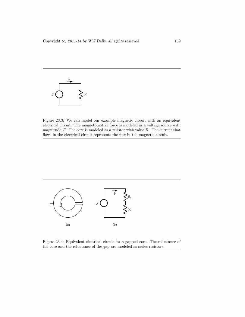
Copyright (c) 2011-14 by W.J Dally, all rights reserved 159
F R
Figure 23.3: We can model our example magnetic circuit with an equivalentelectrical circuit. The magnetomotive force is modeled as a voltage source withmagnitude F . The core is modeled as a resistor with value R. The current thatflows in the electrical circuit represents the flux in the magnetic circuit.
F
Rg
Rc
(a) (b)
Figure 23.4: Equivalent electrical circuit for a gapped core. The reluctance ofthe core and the reluctance of the gap are modeled as series resistors.

160 Green Electronics
F R2
(a) (b)
R1
R3
Figure 23.5: Equivalent electrical circuit for a core with three branches. Eachbranch is modeled as a separate reluctance.
R = Rc +Rg
=lc
µcAc+
lgµ0Ag
(23.13)
Because the permeability of the core is usually much greater (often 1000 timesgreater) than that of free space, we often ignore Rc and approximate the reluc-tance as
R ≈ Rg =lg
µ0Ag(23.14)
We typically assume Ag is the same as Ac near the gap. However, due tofringing fields Rg is usually a slightly lower than would be calculated this way.While fringing flux, and hence gap reluctance, can be approximated analytically,it is more common to use a field solver to compute the fringing flux and gapreluctance numerically.
Figure 23.5 shows a core with three branches (often called an E-core). A coilis wound around one branch - generating MMF F . We model each branch ofthe core with a separate reluctance. All flux from the source flows through thefirst branch R1. This branch includes the entire C-shaped core part left of themiddle column. The flux then splits and flows partly through each of R2 andR3. The middle column is modeled by R2 while the reverse C-shaped sectionto the right of the middle column is modeled by R3. The total reluctance seenby the coil is:
R = R1 +R2||R3 (23.15)
= R1 +R2R3
R2 +R3(23.16)

Copyright (c) 2011-14 by W.J Dally, all rights reserved 161
This results in a total flux of:
φ =FR
(23.17)
=F(R2 +R3)
R1R2 +R1R3 +R2R3(23.18)
This flux is split by the flux divider formed by the reluctance of the right twobranches so that
φ2 = φR3
R2 +R3
=FR3
R1R2 +R1R3 +R2R3(23.19)
φ3 = φR2
R2 +R3
=FR2
R1R2 +R1R3 +R2R3. (23.20)
23.3 Inductance
Changes in i cause changes in φ which in turn induce voltage across our coil.The voltage across each turn of our coil is given by Faraday’s law.
VTurn =dφ
dt(23.21)
So the voltage across the coil of N turns is:
V = Ndφ
dt(23.22)
Substituting (23.5) gives
V =N2
Rdi
dt(23.23)
We refer to the constant N2/R in (23.23) as inductance or L. So we have
L =N2
R(23.24)
L =N2Aµ
l(23.25)
Note that inductance is proportional the cross-sectional area of the magneticcircuit A and inversely proportional to the length of the magnetic path (not thelength of the coil). Adding turns to an inductor increases inductance quadrati-cally.

162 Green Electronics
F1
R
(a) (b)
F2
N1
turns
N2
turns
V1 V2
Figure 23.6: (a) A transformer is created by placing two windings on the samecore so that the flux in the cores passes through both windings. (b) The equiv-alent circuit has a source of MMF for each winding and a reluctance R for thecore.
23.4 Transformers
A transformer (introduced in Section 10.1) is created by arranging two or morewindings so that some or all of the flux through one winding also passes throughthe other winding. Consider the arrangement of two windings, one withN1 turnsand one with N2 turnn, on a toroidal core shown in Figure 23.6(a). Assume fornow that all flux remains in the core and hence passes through both windings.By Faraday’s Law we know that the change in flux induces a voltage in eachturn around the core of Vturn = dφ
dt . Thus we have
V1 = N1dφ
dt(23.26)
V2 = N2dφ
dt(23.27)
V2 =N2
N1V1 (23.28)
The equivalent magnetic circuit for the transformer is shown in Figure 23.6(b).Summing MMF around this loop we can write:
N1i1 −N2i2 = φR (23.29)
If the reluctance were zero we would have the current relationship of an idealtransformer

Copyright (c) 2011-14 by W.J Dally, all rights reserved 163
i2 =N1
N2i2. (23.30)
With non-zero reluctance, however additional current iM flows that is propor-tional to φ. Suppose the secondary were open circuited — i.e., i2 = 0. Then wehave
iM =RN1
φ (23.31)
diMdt
=RN1
dφ
dt(23.32)
diMdt
=RN1
1N1
V1 (23.33)
(23.34)
This current is that due to the magnetizing inductance LM of the transformerwhich, referenced to the primary side, has a value of:
LM =N2
1
R(23.35)
The electric circuit realized by this component is an ideal transformer witha magnitizing inductor with magnitude LM in parallel with the primary, likeFigure 10.3 without the leakage inductance.
Now suppose the transformer the geometry of Figure 23.7(a) where some ofthe flux that passes through the primary coil is diverted through the middlebranch of the circuit and does not link the secondary. The equivalent circuitis shown in Figure 23.7(b). The two windings are represented by two MMFsources F1 and F2. The three branches of the core are represented by threereluctances.
Performing a Y −∆ transformation on the three reluctances gives the circuitof Figure 23.7(c). The three reluctances have values:
RA =R1R2 +R1R3 +R2R3
R∈(23.36)
RB =R1R2 +R1R3 +R2R3
R∞(23.37)
RC =R1R2 +R1R3 +R2R3
R3(23.38)
Reluctance RC here represents the magnetizing inductance of the trans-former. Reluctances RA and RB represent the primary- and secondary-sideleakage inductances respectively.

164 Green Electronics
F1
R1
(b)
F2
(a)
N1
turns
V1 N2
turns
V2
R2
R3
F1
RC
(c)
RA RBF2
Figure 23.7: (a) A transformer with a leakage path for flux that does not linkboth windings. (b) The equivalent circuit has a source of MMF for each windingand three reluctances, one for each branch of the core. (c) A Y −∆ transforma-tion of the reluctances separates the reluctance that determines the magnetizinginductance RC from the reluctances that determine the leakage inductances.

Copyright (c) 2011-14 by W.J Dally, all rights reserved 165
The resulting circuit is an ideal transformer with a magnetizing inductancein parallel with the primary and leakage inductances in series with both the pri-mary and secondary — like Figure 10.3 but with an additional leakage inductorin series with the secondary.
23.5 Exercises
Solve for flux given core geometry and number of turnsSolve for inductance with and without gapSove for flux with complex geometry - multiple branches with and without
gapsSolve for transformer parametersSolve for mag inductanceSolve for leakage inductance

166 Green Electronics

Chapter 24
Magnetic Materials
24.1 Magnetic Materials
In an ideal material there is a linear relationship between B and H, B = µH,as given by (23.10). Real magnetic materials exhibit saturation and hysteresisthat lead to a non-linear B −H characteristic.
24.1.1 Saturation
Magnetic materials with high relative permeability µr can only sustain this highpermeability when the B field is below a maximum level Bsat. Figure 24.1 showsa piecewise linear B − H function that exhibits saturation. Below saturationB = µrµ0H giving a steep slope µrµ0. Above Bsat, the slope is reduced to µ0.Silicon steel has Bsat ≈1.5T. Ferrites have Bsat ≈0.5T.
Magnetic saturation limits the maximum current that can be handled by aninductor.
Imax = Bsatl
Nµ(24.1)
If current i exceeds Imax the incremental permeablility of the material falls by afactor of µr. This causes the inductance to fall by a factor of µr. In an inductorwith an applied voltage, this causes the current to increase µr times faster —often with catastrophic results.
The maximum through current of a transformer is not limited by core sat-uration. The magnetizing current of a transformer (viz. the current flowing inthe magnetizing inductance) is limited by (24.1).
Figure 24.1 shows an abrupt transition in incremental permeability (theslope of the B-H curve) at Bsat. While some magnetic materials have such ahard transition, in other materials the transition is more gradual. For example,Figure 24.2 shows the B-H curve for a Ferroxcube ferrite this material has aninitial permeability of µr = 3000 and saturates gradually at 0.4T at 100C. In
167

168 Green Electronics
H (A/m)
B (T)
Bsat
Bsat
Ideal B-H
Curve
B-H curve with
saturation
Figure 24.1: B-H curves with and without saturation. Above the saturationflux density Bsat the permeability, and hence the slope of the curve, is reducedfrom µrµ0 to µ0.
practice one would not operate cores build from this material with a B fieldabove 0.3T.
The B-H curve in Figure 24.2 also has hysteresis which we shall discuss inthe next section.
24.1.2 Hysteresis
A ferromagnetic material has memory1. When a strong B field is applied to thematerial, it becomes magnetized. That is, it behaves like a permanent magnet.When a material is magnetized, the B field is given by:
B = µ(H +M) (24.2)
The magnetization M provides a MMF in the magnetic circuit, just like a wind-ing carrying current.
Consider a cycle of a magnetic component. Initially a high negative Hfield is applied to the component this causes magnetic domains to aligh so thatM = −Hc. As H is increased the B field follows the right side of the curve ofFigure 24.3. When H = Hc, B = µ(H + M) = 0. That is, we have to applya magnetic field of Hc, called the coercivity of the material, to zero the fluxdensity. For silicon steel Hc ≈ 40 A/m. For ferrites Hc ≈ 10 A/m.
1At one time, almost all computers used magnetic-core memories based on this principle.

Copyright (c) 2011-14 by W.J Dally, all rights reserved 169
Figure 24.2: B-H curves for Ferroxcube 3C95 ferrite material at 25C and 100C.These curves exhibit both saturation and hysteresis and have a soft saturationcharacteristic.

170 Green Electronics
H (A/m)
B (T)
Bsat
Bsat
Hc
Br
Figure 24.3: A B-H curve with hysteresis. Initially the core is magnitized withM = −Hc so that an H-field of Hc is required to bring the flux density to 0.After driving the core to saturation the magnetiztion is reversed to M = Hc sothat when the H-field is removed a residual flux density of Br remains.
As we increase H above Hc, the B field goes positive and we continue tomove up the right side of the curve in Figure 24.3. When B = Bsat the coresaturates. At this high field, the magnetic domains in the material reverse andM = Hc.
With positive magnetization, as we bring the H field back to zero we nowfollow the left side of the curve in Figure 24.3 as we reduce H. When H = 0, aresidual flux density Br = µHc remains.
As we continue to reduce H below zero we follow the left side of the curveof Figure 24.3 until we reach B = −Bsat. At this high negative field the mag-netization reverses so that M = −Hc and we start the cycle over again.
Hysteresis in the B-H curve causes core losses. Each cycle around the B-Hloop dissipates energy proportional to the area of the loop and the volume ofthe core. To see this note that:
v =dφ
dt= A
dB
dt(24.3)
i = lH (24.4)
P = vi = AlHdB
dt(24.5)
E =∫Pdt = Al
∫HdB (24.6)

Copyright (c) 2011-14 by W.J Dally, all rights reserved 171
Figure 24.4: Loss per unit volume, PV , for Ferroxcube 3C95 material at 100kHz,200kHz, and 400kHz.
Here Al is the volume of the core — the product of its area and length. Theintegral
∫HdB over one cycle is the area of the loop.
The actual B-H curve, and hence the core loss, varies with frequency fand Bmax. Figure 24.4 shows the core loss per unit volume (kW/m3) for theFerroxcube 3C95 material at three frequencies. This relationship between loss,frequency, and Bmax can also be described as a power law:
PV = KfαBβmax. (24.7)
For Magnetics Inc. R material, for example, K =36, α = 1.64, and β =2.68— with PV in units of W/m3.

172 Green Electronics
24.2 Exercises
simulate inductor saturatingcalculate loss in one cycle of B-H curvecalculate core loss for typical situation

Chapter 25
Wire for Magnetics
Our magnetic components, inductors and transformers, are realized by windingconductive wire on a core of magnetic material. Most often the winding ismade using copper magnet wire — bare copper wire with a very thin layer ofinsulating material. However copper tape, bar, and tube and conductors madefrom aluminum may be used in certain situations. The conductivity of the wirematerial and wire cross-section area determine the DC resistance of the winding.
For many green electronics applications, however, the AC performance of themagnetic component is important. Typical operating frequencies for switchingpower converters run from 10s of kHz to low MHz. At these frequencies theskin effect and proximity effect cause the bulk of the AC current to flow in athin layer on the surface of the conductor. This causes the AC conductivity of awire to increase only linearly with radius. At high frequencies thick (low gauge)wires waste copper and magnetic core window area.
A solution to the problem of AC conductivity is to realize a winding withmany parallel, fine-gauge strands of wire. The diameter of each strand is chosenso that the bulk of the wire area carries current. In some cases Litz wire whichconsists of many parallel, fine-grain strands braided together may be employed.
25.1 Skin Effect
AC current in a wire flows primarily in a narrow layer near the surface of thewire with the current density falling off exponentially with depth according to:
J = J0exp
(d
δ
)(25.1)
The skin depth δ is the the depth at which the current has fallen off to exp−1of its starting magnitude and is given by:
173

174 Green Electronics
δ =√
ρ
πfµ(25.2)
Where ρ is the conductivity of the wire material and f is the frequency of theAC current. From (25.2) we see that δ is proportional to f−1/2. For copper at100kHz the skin depth is about 0.2mm.
Above a skin-depth frequency fs, a wire of radius r can be considered to becarrying current uniformly over its entire cross section.
fS =ρ
πµr2(25.3)
Below fs the AC and DC resistance of the wire are identical. Above fs the ACresistance becomes appreciably larger than the DC resistance of the wire and isgiven by:
RAC = RDC
(max 1,
√f
fS
)(25.4)
AC current in a wire generates a time varying magnetic field that penetratesthe wire. This field, in turn, opposes the flow of current in the core of the wire.This results in the distribution of current given by (25.1) (which can be derivedfairly easily from Maxwell’s equations).
To avoid having high AC resistance, or wasting copper, or both, we choosethe radius of the wire to satisfy (25.3) so that:
r < rs = sqrtρ
πµf(25.5)
25.2 Proximity Effect
l =2nNrw
(25.6)
RAC = RDC
(1 +
(πnN)2 r6
12δ4w2
)= RDC
(1 +
(πl)2
12
(rδ
)4)
= RDC
(1 +
(πl)2
12
(f
fS
)2)
(25.7)
25.3 Litz Wire
25.4 Winding Geometry
inter-winding capacitanceinterleaving primary and secondary

Copyright (c) 2011-14 by W.J Dally, all rights reserved 175
25.5 Exercises

176 Green Electronics

Chapter 26
Designing MagneticComponents
[need to talk about wire before this]Now that we understand the basics of magnetic circuits and the proper-
ties of magnetic materials we are prepared to discuss how to design magneticcomponents: inductors and transformers.
26.1 Inductor Design
The process of inductor design starts with a specification and a set of opti-mization constraints. The specification typically includes the inductance L, theoperating frequency f , the maximum current Imax, and the RMS current IRMS.The optimization constraints deal with the tradeoff between cost and powerloss. In some cases we want to design the lowest cost inductor that has lossesless than a specified maximum PLmax. In other cases we want the inductor withthe lowest possible loss below a given maximum cost.
In some cases, some of our specification variables may be part of a largeroptimization. For example, in the design of a switching converter, one may varyswitching frequency f to trade off switching losses against core losses. For now,however, we will consider f to be fixed by the specification.
Given a specification and an optimization constraint inductor design is aniterative process involving the following steps — using a spreadsheet or Matlabto perform the optimization.
1. Pick a core.
2. Calculate the gap g and number of turns N required to achieve inductanceL on this core as a function of Bmax.
3. Select a wire gauge and compute the number of parallel strands that willfit on the core — also as a function of Bmax.
177
178 Green Electronics
4. Perform an optimization to find the Bmax that gives the lowest loss on thiscore. As Bmax is swept one trades off core loss against wire loss. Minimumloss typically happens at the point where the two are roughly balanced.
5. Iterate steps 1-4 over other cores to optimize the solution.
To compute the number of turns required to realize an inductance of L witha maximum current of Imax and flux density of Bmax we substitute (23.24) into(23.8) at this operating point and derive:
Bmax =NImax
AR(26.1)
BmaxAR = NImax (26.2)
BmaxAN2
L= NImax (26.3)
N =LImax
BmaxA(26.4)
We see that the number of turns requires decreases with Brmmax and increaseswith Imax.
To determine lg, the length of the gap needed we assume that all of R isacross the gap. Substituting (23.24) into (23.14) we write:
R =lg
µ0Ag(26.5)
N2
L=
lgµ0Ag
(26.6)
lg =N2µ0Ag
L(26.7)
26.2 Inductor Example
26.3 Transformer Design
26.4 Exercises

Copyright (c) 2011-14 by W.J Dally, all rights reserved 179
Part III. Motor Control
Brushed PM motorMotor ControlBrushless PM motorAC Induction motor

180 Green Electronics
Chapter 27
Electric Motors
Many green electronic systems involve the conversion between mechanical en-ergy and electrical energy. A wind turbine converts mechanical energy (from thewind) to electrical energy to drive the grid. An electric car converts mechan-ical energy (from the car’s battery) to mechanical energy (to propel the car)and then back again (during regenerative braking). The device most commonlyused to convert from electrical to mechanical energy is a motor. We refer tothis device as a generator when it is used in the opposite direction — to convertfrom mechanical to electrical.
In this chapter we introduce the basic concepts of electric motors and gener-ators by examining the operation and control of a brushed permanent magnetmotor.
27.1 Lorentz Force and Faraday Induction
The force generated by a motor is due to the Lorentz force that is generated bya moving charge in a magnetic field.
F = q (v ×B) (27.1)
Where F (the force), B (the magnetic field), and v (the charge velocity) are3-vectors, and q (the charge) is a scalar. If the charges are confined to a wirewe can rewrite this as
F = i (L×B) (27.2)
Where L is a 3-vector representing the length and direction of the wire and i isthe scalar current.
Figure 27.1 shows (27.2) graphically. Here the B field is to the left andthe current is flowing away from the viewer. The resulting force is upward —perpendicular to both B and L following the right-hand rule.
181
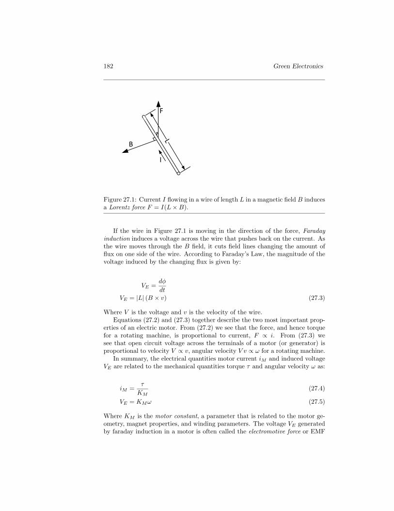
182 Green Electronics
B
I
F
L
Figure 27.1: Current I flowing in a wire of length L in a magnetic field B inducesa Lorentz force F = I(L×B).
If the wire in Figure 27.1 is moving in the direction of the force, Faradayinduction induces a voltage across the wire that pushes back on the current. Asthe wire moves through the B field, it cuts field lines changing the amount offlux on one side of the wire. According to Faraday’s Law, the magnitude of thevoltage induced by the changing flux is given by:
VE =dφ
dtVE = |L| (B × v) (27.3)
Where V is the voltage and v is the velocity of the wire.Equations (27.2) and (27.3) together describe the two most important prop-
erties of an electric motor. From (27.2) we see that the force, and hence torquefor a rotating machine, is proportional to current, F ∝ i. From (27.3) wesee that open circuit voltage across the terminals of a motor (or generator) isproportional to velocity V ∝ v, angular velocity V v ∝ ω for a rotating machine.
In summary, the electrical quantities motor current iM and induced voltageVE are related to the mechanical quantities torque τ and angular velocity ω as:
iM =τ
KM(27.4)
VE = KMω (27.5)
Where KM is the motor constant, a parameter that is related to the motor ge-ometry, magnet properties, and winding parameters. The voltage VE generatedby faraday induction in a motor is often called the electromotive force or EMF
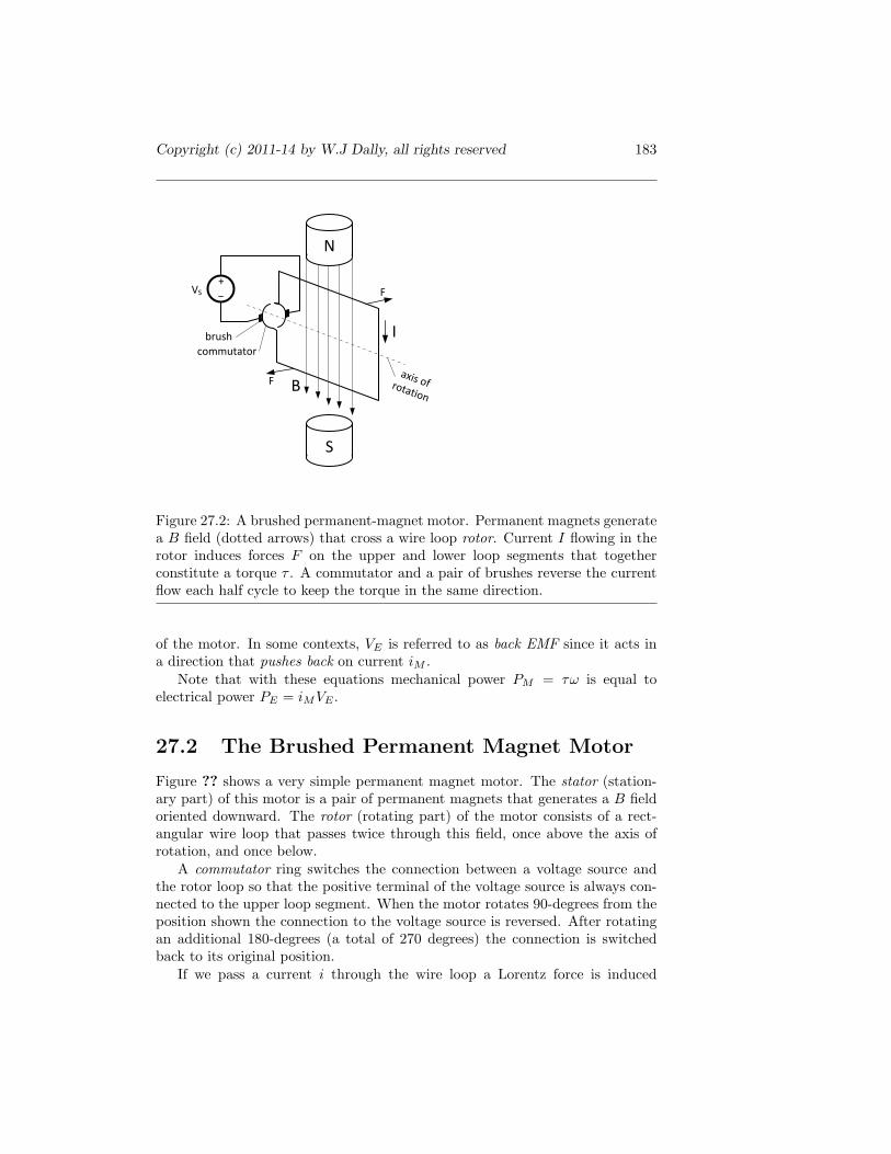
Copyright (c) 2011-14 by W.J Dally, all rights reserved 183
S
N
B
I
VS
+
axis of rotation
commutator
brush
F
F
Figure 27.2: A brushed permanent-magnet motor. Permanent magnets generatea B field (dotted arrows) that cross a wire loop rotor. Current I flowing in therotor induces forces F on the upper and lower loop segments that togetherconstitute a torque τ . A commutator and a pair of brushes reverse the currentflow each half cycle to keep the torque in the same direction.
of the motor. In some contexts, VE is referred to as back EMF since it acts ina direction that pushes back on current iM .
Note that with these equations mechanical power PM = τω is equal toelectrical power PE = iMVE .
27.2 The Brushed Permanent Magnet Motor
Figure ?? shows a very simple permanent magnet motor. The stator (station-ary part) of this motor is a pair of permanent magnets that generates a B fieldoriented downward. The rotor (rotating part) of the motor consists of a rect-angular wire loop that passes twice through this field, once above the axis ofrotation, and once below.
A commutator ring switches the connection between a voltage source andthe rotor loop so that the positive terminal of the voltage source is always con-nected to the upper loop segment. When the motor rotates 90-degrees from theposition shown the connection to the voltage source is reversed. After rotatingan additional 180-degrees (a total of 270 degrees) the connection is switchedback to its original position.
If we pass a current i through the wire loop a Lorentz force is induced

184 Green Electronics
LM RM
V =KMVM
+
-
iM
CM = IM/KM RF = 1/KF
+
iL= LKM2
Figure 27.3: Electrical model of a brushed permanent magnet motor. VM is thevoltage applied at the motor terminals. Elements LM and RM represent theinductance and resistance of the rotor winding. Capacitor CM represents theinertia of the rotor. Resistor RF represents the friction of the motor. Currentsource iL represents the load on the motor. The voltage across CM , RF , andiL is VE = KMω, the EMF of the motor.
according to (27.2) in the upper and lower segments of the rotor. The force inthe upper segment is into the page and the force in the lower segment is out ofthe page so that collectively they generate a torque about the axis of rotation.The magnitude of this torque is proportional to the current as per (27.4).
If we disconnect the voltage source and rotate the motor, Faraday inductiongenerates a voltage across our rotor according to (27.3). The commutator en-sures that the positive induced voltage is always on the upper terminal of thedisconnected source. As per (27.5) the magnitude of this voltage is proportionalto the angular velocity of the motor ω.
An actual motor is slightly more complex than what we have described here.Rather than a single loop in the rotor, it has several loops spaced by a smallnumber of degrees so that the torque generated by the motor is approximatelyconstant with angle. With a single loop the torque is a rectified sine wave.That is, the torqe at angle θ is proportional to | sin(θ)|. With multiple loopsthe torque is approximately constant, independent of angle.
The rotor of an actual motor also typically has a laminated steel core toprovide a low reluctance path for the magnetic field to give a larger B fieldacross a relatively short gap between the magnets in the stator and the rotorcore. The fields and forces across the gap are complex, vary slightly with angle,and are usually modeled using field solvers. To a very good approximation,however, the motor V-I characteristics are still governed by (27.5) and (27.4).
27.3 Motor Model
For the purposes of motor control, we model a motor as shown in Figure 27.3.The two horizontal elements, RM and LM represent the resistance and induc-tance of the rotor windings. When a voltage VM is applied to the motor ter-

Copyright (c) 2011-14 by W.J Dally, all rights reserved 185
minals, a current iM flows giving a drop of iMRM + LMdiM
dt across the rotorwindings. The voltage left after these winding drops is VE , the EMF of themotor caused by faraday induction.
VE = VM − iMRM − LMdiMdt
= KMω (27.6)
The inertia of the motor is modeled by capacitor CM . A torque τI = IMdωdt
is required to accelerate the motor. Substituting (27.4) this torque requires acurrent
iI =IM
KM
dω
dt
=IM
K2M
d∨E
dt(27.7)
So the capacitance required to model the moment of inertia IM is
CM =IMK2
M
(27.8)
We model the internal friction of the motor as resistor RF = 1KF
. Thisfriction draws a current iF = VE
RF= VEKF and hence has a torque of τF =
VEKFKM .Finally, the load on the motor is modeled as a current source, iL = τLKM .
In some cases we may use a more sophisticated model for the load. For example,in an electric vehicle we may use a capacitor to model the momentum of thevehicle, a resistor to model the friction of the vehicle, and a current source torepresent changes in elevation.And the kinetic energy stored in the inertia of the rotor is modeled by the energystored in the capacitor.
EI =12IMω2 =
12CMV 2
E (27.9)
27.4 The Torque Curve
We can characterize the steady-state response of a motor with a fixed appledvoltage VM as a torque-speed curve. As shown in Figure 27.4 this curve showsthe torque the motor is delivering to the load as a function of motor speed.
At one extreme, if there is no load on the motor (zero torque), and if weignore motor friction, VE = VM and
ωmax =VM
KM(27.10)

186 Green Electronics
Anguar Velocity (rad/s)
Torq
ue
(N
m)
0
max
max
Figure 27.4: Torque vs speed curve for an electric motor. For a given appliedvoltage, the motor is characterized by its locked rotor torque τ0, and its unloadedspeed ωmax. Thermal limits often impose a maximum torque τmax < τ0.

Copyright (c) 2011-14 by W.J Dally, all rights reserved 187
LM 2 mHRM 0.22 ΩKM 0.66 V s
rad
IM 0.083
Table 27.1: Parameters for a typical brushed, permanent-magnet DC motor.
If we take friction, modeled by RF into account, we get the expression
ωmax =RFVM
(RF +RM )KM(27.11)
Thus, if we ignore friction (or if we know both RF and RM ) we can derive themotor constant KM from the unloaded speed ωmax.
At the other extreme, if the rotor is stationary, VE = KMω = 0 and so thecurrent drawn by the motor is IM = VM
RM. Hence the locked-rotor torque is
τ0 = KMIM =KMVM
RM(27.12)
Thus, if we know RM we can also derive KM from a measurement of τ0,or alternately if we know KM we can determine RM from τ0. Note that theeffective resistance here is the entire resistance around the loop that connectsthe source to the motor, not just the winding resistance of the motor. Theeffective resistance includes, for example, the internal resistance of the sourceand the resistance of the wires connecting the source to the motor.
For many motors, passing a current i0 = VM
RMthrough the rotor windings for
more than a very short period of time will result in destructive temperatures.To avoid burning out the motor, we often cap the torque curve at a maximumcontinuous torque τmax that corresponds to a maximum continuous current imax.It is possible to exceed this value for short periods of time as long as the motorcomponents are kept within their safe temperature zones.
27.5 Step Response
The step response of an unloaded motor is determined by its electrical andmechanical time constants, and observing the response can help determine themotor parameters. In this section we develop a Matlab model of a typical motorand using this model simulate the motor’s step response. The parameters of ourmotor are listed in Table 27.5.
We simulate one time step dt of motor operation using the code shown inFigure 27.5. The two state variables are inductor current i m and motor velocityomega. This code computes the back EMF of the motor VE and from this thedrop across the inductor VL. The inductor voltage is integratd to give the next
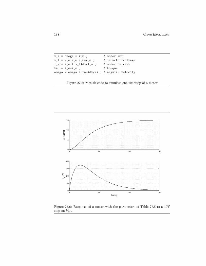
188 Green Electronics
v_e = omega * k_m ; % motor emfv_l = v_m-v_e-i_m*r_m ; % inductor voltagei_m = i_m + v_l*dt/l_m ; % motor currenttau = i_m*k_m ; % torqueomega = omega + tau*dt/mi ; % angular velocity
Figure 27.5: Matlab code to simulate one timestep of a motor
0 50 100 1500
10
20
30
40
i M (A
)
t (ms)
0 50 100 1500
5
10
15
t (r
ad/s
)
Figure 27.6: Response of a motor with the parameters of Table 27.5 to a 10Vstep on VM .

Copyright (c) 2011-14 by W.J Dally, all rights reserved 189
value of inductor current IM . Torque τ which is proportional to IM is thenintegrated to give the next value of ω.
The response of our simulated motor to a 10V step in input voltage is shownin Figure 27.6. The figure shows ω on the top panel and IM on the bottompanel. Motor inductance LM can be determined from the initial slope of thecurrent curve. At this point ω = 0 and IM = 0 so VE = 0 and VR = RMIM = 0so the entire VM drops across LM thus we have:
LM =VM
di/dt(27.13)
In this case VM = 10V and the initial slope di/dt = 5A/ms so we have LM =2mH which is consistent with Table 27.5.
Ignoring friction we can determine KM from the steady state value of ω. Inthis case we have ω = 15rad/s at VE = 10V so we have KM = VE/ω = 0.66.
Once KM is known, the moment of inertia can be determined from the ratioof τ and dω/dt at any point on the curve. At 19ms, for example the currentreaches a peak value of 34.5A corresponding to a torque of 22.8Nm and dω/dt =275rad/s2. This gives IM =.083Nms2/rad.
Finally, the time constant on the tail of the curve, about 40ms, is equal toτM = RMCM so we have:
RM =τMCM
(27.14)
=τMK2
M
IM(27.15)
(27.16)
Plugging in our estimated values of τM = 40ms, KM=0.66, and IM=0.083.We get RM = 0.21Ω which is off slightly because we have mis-estimated τM .Its actual value is 42ms.
27.6 Motor Drive
A motor drive is a circuit used to apply current and voltage to the terminals ofa motor. A simple motor drive, shown in Figure 27.7, is just a voltage source V1
and a switch. The switch is used as a half-bridge to connect one motor terminalto either the supply voltage V1 or to ground.
This configuration is really a (Chapter 2) where the inductor and capacitorare provided by LM and CM of the motor itself. If the switch is operated widtha duty factor of D in position a, then the effective voltage seen by the motorterminals is
VM = DV1 (27.17)
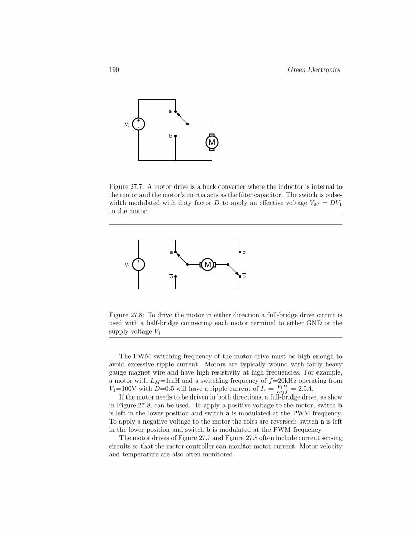
190 Green Electronics
V1
+
-
a
b
M
Figure 27.7: A motor drive is a buck converter where the inductor is internal tothe motor and the motor’s inertia acts as the filter capacitor. The switch is pulse-width modulated with duty factor D to apply an effective voltage VM = DV1
to the motor.
V1
+
- M
a
a
b
b
Figure 27.8: To drive the motor in either direction a full-bridge drive circuit isused with a half-bridge connecting each motor terminal to either GND or thesupply voltage V1.
The PWM switching frequency of the motor drive must be high enough toavoid excessive ripple current. Motors are typically wound with fairly heavygauge magnet wire and have high resistivity at high frequencies. For example,a motor with LM=1mH and a switching frequency of f=20kHz operating fromV1=100V with D=0.5 will have a ripple current of Ir = V1D
LM f = 2.5A.If the motor needs to be driven in both directions, a full-bridge drive, as show
in Figure 27.8, can be used. To apply a positive voltage to the motor, switch bis left in the lower position and switch a is modulated at the PWM frequency.To apply a negative voltage to the motor the roles are reversed: switch a is leftin the lower position and switch b is modulated at the PWM frequency.
The motor drives of Figure 27.7 and Figure 27.8 often include current sensingcircuits so that the motor controller can monitor motor current. Motor velocityand temperature are also often monitored.

Copyright (c) 2011-14 by W.J Dally, all rights reserved 191
In some cases rather than directly measuring a parameter we estimate theparameter from other measurements. Motor velocity, ω, for example, can beesimated by measuring the voltage across the motor with no current applied.Even if current is applied, we can estimate VE and hence ω if we know thecurrent and subtract the drops across LM and RM from the applied VM .
27.7 Exercises
model an actual motorequivalent capacitance

192 Green Electronics

Chapter 28
Motor Control
In addition to a motor drive (Section 27.6) a controller is needed to drive a motorto a desired state. Depending on the application we may drive the motor to adesired position, a desired velocity, or to apply a desired torque. For example,a motor controlling an air vent may be commanded to a particular position Θcorresponding to the vent being open or closed. When a motor is geared, thisposition may involve a number of revolutions, not just an angle between 0 and2π. When a cruise control is engaged, a motor may be controlled to a constantvelocity ω. Finally, the controller in an electric vehicle may drive the motor toproduce a torque that is a function of the position of the accelerator pedal.
In performing its control functions, the controller may make use of sensorsthat measure the motor position, velocity, and/or torque. Current sensors areoften used to approximately measure motor torque, and measures or estimatesof back EMF VE may be used to approximate velocity.
In this chapter we develop a simple controller for motor velocity. We thenmodify this controller to operate within the constraints of a current limit.
28.1 A Naive Controller
Suppose we have a motor with the parameters shown in Table 27.5 and wewish to command it to operate at 30rad/s for 0.3s 20rad/s for 0.3s followed by40 rad/s for 0.3s. Further assume that our motor has a strict current limit ofImax =20A. That is |IM | < Imax at all times.
The simplest approach is to use an open-loop controller that applys thecontrol law:
VM = KMωd (28.1)
Where ωd is the desired velocity.Our controller, of course sets D, not VM by applying (27.17) to give D =
VM/V1. Because it is simpler, we will deal with VM for the remainder of this
193

194 Green Electronics
0 0.1 0.2 0.3 0.4 0.5 0.6 0.7 0.8 0.90
20
40
t (r
ad/s
)
0 0.1 0.2 0.3 0.4 0.5 0.6 0.7 0.8 0.90
10
20
30
v M (V
)
0 0.1 0.2 0.3 0.4 0.5 0.6 0.7 0.8 0.9−50
0
50
100
i M (A
)
t (s)
Figure 28.1: Response of our example motor to the naive control law of (28.1).
discussion of control. It is understood that what is actually being set by thedrive is D.
The response of simulating our example motor with the naive control lawof (28.1) is shown in Figure 28.1. At time zero we step VM to 19.8V and themotor slowly responds by winding up to 30rad/s. At 0.3s we apply 13.2V andthe motor responds by slowing to 20rad/s. At 0.6s we apply 26.4V and themotor accelerates to 40rad/s.
We refer to the process that starts at 0.3s as regenerative braking. At 0.3swe drop VM to 13.2V and the motor slows to 20rad/s. By applying VM < VE ,negative current flows and torque is applied in a direction opposite the rotationof the motor — braking the motor. During this period the motor is acting as agenerator with power flowing from the motor to supply V1. We could brake themotor harder — apply a stronger reverse torque — by dropping VM even lower,or by applying a negative VM using the drive of Figure 27.8.
While we think of the motor drive as a buck converter — with the inductorand capacitor provided by the equivalent circuit of the motor, during regener-ative braking the drive is acting as a boost converter. During this period itis taking current at a potential of VE and boosting it to V1 to return energyto the supply. The motor’s inductance LM serves as the inductor of the boostconverter.

Copyright (c) 2011-14 by W.J Dally, all rights reserved 195
err = omega_d - omega ;ierr = ierr + err*dt ;v_m = err*p + ierr*q ;
Figure 28.2: Matlab code for PI control law
Looking just at the ω panel of the figure our naive approach to motor controldoesn’t look too bad. The motor goes to each commanded speed with a delaydetermined by the motor time constant τM = RMCM . In fact this plot is justthree copies of the motor step response Figure 27.6 appropriately translated.
Unfortunately this naive control scheme has two problems. First it exceedsour current limit by a large margin in both directions. Current IM reachesextreme values of +90A and -30A. Second, ignoring the current for the moment,the response is not as fast as it could be with a more sophisticated controller.
28.2 PI Motor Control
Since our motor drive is really just a buck converter we can apply the PI controllaw we developed in Chapter 5 to control this drive. Regulating the velocityω of the motor is exactly analgous to regulating the output voltage VC of thebuck regulator. The Matlab code for a PI control law for our motor is shownin Figure 28.2. We leave the derivation of the gain constants p and q as anexercise.
The simulated response of our example motor to the PI control law is shownin Figure 28.3. The good news is that with the PI controller the motor responseis much faster. However, achieving this fast response has made our over-currentproblem even worse. Current IM now has extremes of 245A and -80A.
28.3 Current-Limited Control
To achieve a rapid motor response while staying within our current limit requiresthat we regulate motor current. One approach to this is shown in the Matlabcode of Figure 28.4. Here we assume we have exact knowledge of ω, RM , andKM and hence can compute bounds on VM that we must stay within to preventexcessive current. The control code computes VM using a PI control law, justas in Figure 28.2 and then clamps VM to the calculated limits.
The last three lines of code are needed to prevent a control pathology knownas integral wind up. If the control output of a controller with an integral errorterm is clamped (as we are doing here), the integral error will continue to growwithout bound. When the clamp is eventually released the large integral errorwill cause an overshoot, often quite large, in the response. To avoid integralwindup, whenever our clamp overrides the value of VM , we also clamp ierr tothe value that would produce our clamped VM if there were no proportional

196 Green Electronics
0 0.1 0.2 0.3 0.4 0.5 0.6 0.7 0.8 0.90
20
40
60
t (r
ad/s
)
0 0.1 0.2 0.3 0.4 0.5 0.6 0.7 0.8 0.90
20
40
60
v M (V
)
0 0.1 0.2 0.3 0.4 0.5 0.6 0.7 0.8 0.9−100
0
100
200
300
i M (A
)
t (s)
Figure 28.3: Response of our example motor to the PI control law of Figure 28.2.Response is faster than the naive control law but the excess current problem iseven larger.
% original PI controllererr = omega_d - omega ;ierr = ierr + err*dt ;v_m_1 = err*p + ierr*q ;
% now apply current limitv_m_max = i_max*r_m + v_e ;v_m_min = -i_max*r_m + v_e ;v_m = min(v_m_max, max(v_m_min, v_m_1)) ;if(v_m ~= v_m_1)ierr = v_m/q ;
end
Figure 28.4: Matlab code for PI control law with current limiting. The overrideof ierr is used to prevent integral wind up when the control is limited.
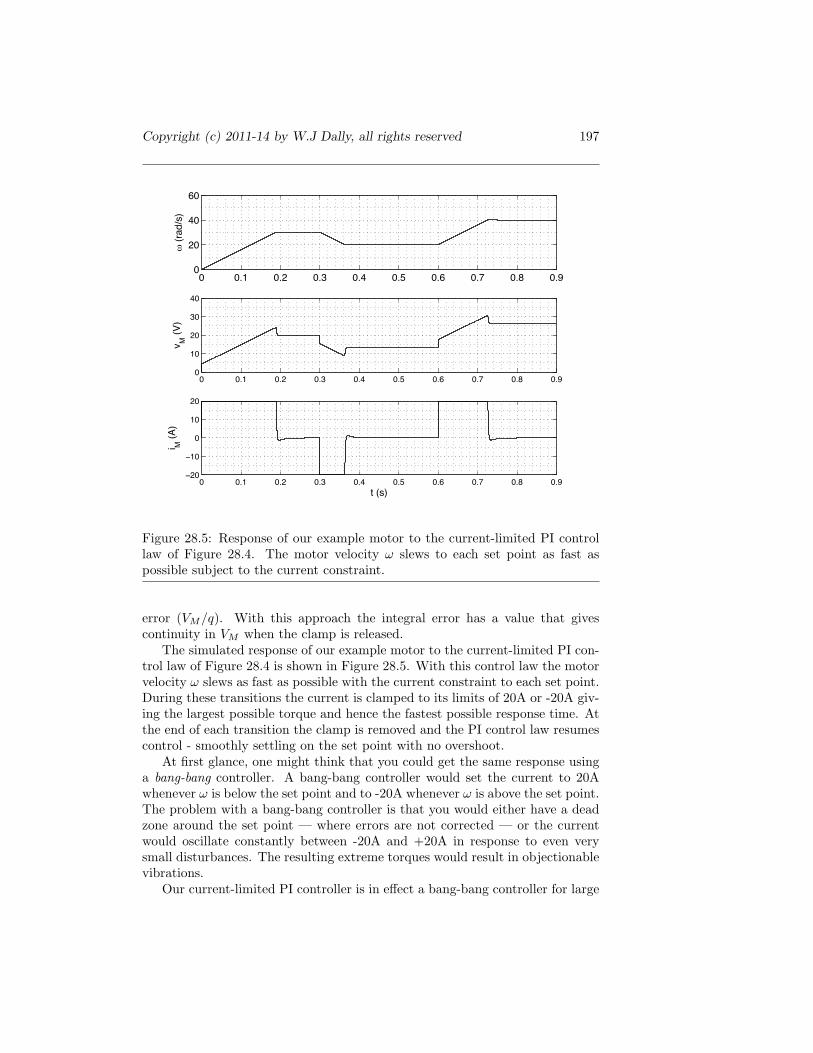
Copyright (c) 2011-14 by W.J Dally, all rights reserved 197
0 0.1 0.2 0.3 0.4 0.5 0.6 0.7 0.8 0.90
20
40
60
t (r
ad/s
)
0 0.1 0.2 0.3 0.4 0.5 0.6 0.7 0.8 0.90
10
20
30
40
v M (V
)
0 0.1 0.2 0.3 0.4 0.5 0.6 0.7 0.8 0.9−20
−10
0
10
20
i M (A
)
t (s)
Figure 28.5: Response of our example motor to the current-limited PI controllaw of Figure 28.4. The motor velocity ω slews to each set point as fast aspossible subject to the current constraint.
error (VM/q). With this approach the integral error has a value that givescontinuity in VM when the clamp is released.
The simulated response of our example motor to the current-limited PI con-trol law of Figure 28.4 is shown in Figure 28.5. With this control law the motorvelocity ω slews as fast as possible with the current constraint to each set point.During these transitions the current is clamped to its limits of 20A or -20A giv-ing the largest possible torque and hence the fastest possible response time. Atthe end of each transition the clamp is removed and the PI control law resumescontrol - smoothly settling on the set point with no overshoot.
At first glance, one might think that you could get the same response usinga bang-bang controller. A bang-bang controller would set the current to 20Awhenever ω is below the set point and to -20A whenever ω is above the set point.The problem with a bang-bang controller is that you would either have a deadzone around the set point — where errors are not corrected — or the currentwould oscillate constantly between -20A and +20A in response to even verysmall disturbances. The resulting extreme torques would result in objectionablevibrations.
Our current-limited PI controller is in effect a bang-bang controller for large

198 Green Electronics
errors (where the current limit takes effect) but transitions smoothly to a linearcontrol law for small errors. Hence it suffers from neither a dead zone nor fromoscillating current — and torque — extremes.
Figure 28.4 clamps current by computing a set of voltage limits that corre-spond to the current limits and then clamping VM to these limits. An alternateapproach, that can be used when motor parameters are not exactly known, isto build a current regulator that runs in parallel with the velocity regulator.Whenever IM is within limits the velocity regulator sets VM . The current reg-ulator takes over when IM exceeds the current limit. We leave implementingsuch a current regulator as an exercise.
28.4 Exercises
derive the coefficientsrun the current limit controller without integral wind up preventionbuild a current regulatordevelop a controller for motor position simulate in Matlabdevelop a controller for motor torque simulate in Matlab
Chapter 29
Brushless PermanentMagnet Motors
While the brushed permanent magnet motor is simple to understand and tocontrol it has the disadvantage of having a commutator and brushes. Theseparts add to the expense of the motor and the brushes wear out with operationrequiring service.
The brushless permanent magnet motor eliminates the commutator andbrushes and replaces them by electronic swithches that connect the windings(which are moved to the stator) to the supply. The behavior of the brushlesspermanent magnet motor is exactly the same as the brushed motor with oneexception: the applied voltage and current must be rotated so they are perpen-dicular to the current position of the rotor. This is done by modulating the driveto multiple, usually three, phases. As long as this orientation is maintained, thebehavior is exactly as described in Chapter 27: torque is proportional to currentand voltage is proportional to angular velocity.
In this chapter we introduce the brushless permanent magnet motor. Weshow how it can be driven either using hard commutation or by synthesizing amulti-phase sine wave using an inverter Chapter 15. We adapt our motor driveSection 27.6 and our motor control methods Chapter ?? to brushless motors.
29.1 Motor Geometry
Figure 29.1 shows a brushless permanent magnet motor in schematic form. Theroles of the stator and rotor are reversed compared to the brushed motor ofFigure 27.2. With the brushless motor the rotor contains the permanent magnetand the stator contains the windings. The windings are divided into multiplephases — three in this case — to control the direction of the applied field.
To analyze the brushless motor we can consider separately the field andtorque produced by the phase currents and the back EMF voltage induced bythe rotating magnet. Let us first consider the back EMF.
199

200 Green Electronics
N
S
1
23
Figure 29.1: A three-phase brushless permanent-magnet motor has a statorwith three windings that generate a rotating magnetic field. The rotor containsa permanent magnet that generates torque in response to the stator’s magneticfield. As the permanent magnet rotates, it also induces voltage in the statorwindings.
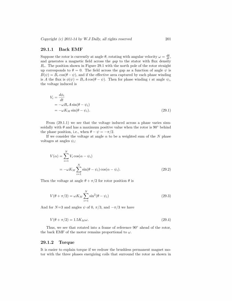
Copyright (c) 2011-14 by W.J Dally, all rights reserved 201
29.1.1 Back EMF
Suppose the rotor is currently at angle θ, rotating with angular velocity ω = dθdt ,
and generates a magnetic field across the gap to the stator with flux densityBr. The position shown in Figure 29.1 with the north pole of the rotor straightup corresponds to θ = 0. The field across the gap as a function of angle ψ isB(ψ) = Br cos(θ−ψ), and if the effective area captured by each phase windingis A the flux is φ(ψ) = BrA cos(θ − ψ). Then for phase winding i at angle ψi,the voltage induced is
Vi =dφi
dt= −ωBrA sin(θ − ψi)= −ωKM sin(θ − ψi). (29.1)
From (29.1.1) we see that the voltage induced across a phase varies sinu-soidally with θ and has a maximum positive value when the rotor is 90 behindthe phase position, i.e., when θ − ψ = −π/2.
If we consider the voltage at angle α to be a weighted sum of the N phasevoltages at angles ψi:
V (α) =N∑
i=1
Vi cos(α− ψi)
= −ωKM
N∑i=1
sin(θ − ψi) cos(α− ψi). (29.2)
Then the voltage at angle θ + π/2 for rotor position θ is
V (θ + π/2) = ωKM
N∑i=1
sin2(θ − ψi) (29.3)
And for N=3 and angles ψ of 0, π/3, and −π/3 we have
V (θ + π/2) = 1.5KMω. (29.4)
Thus, we see that rotated into a frame of reference 90 ahead of the rotor,the back EMF of the motor remains proportional to ω.
29.1.2 Torque
It is easier to explain torque if we redraw the brushless permanent magnet mo-tor with the three phases energizing coils that surround the rotor as shown in
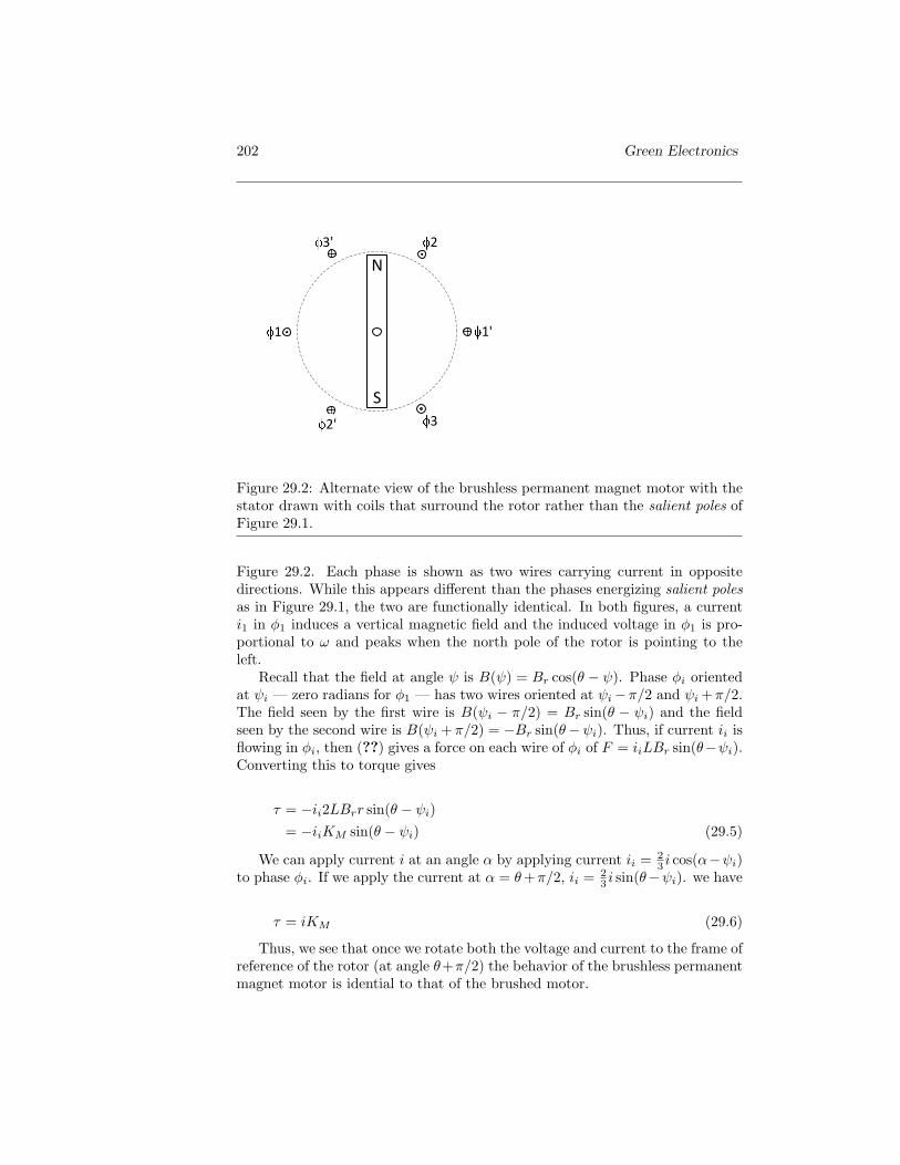
202 Green Electronics
N
S
1
2
3
1'
2'
3'
Figure 29.2: Alternate view of the brushless permanent magnet motor with thestator drawn with coils that surround the rotor rather than the salient poles ofFigure 29.1.
Figure 29.2. Each phase is shown as two wires carrying current in oppositedirections. While this appears different than the phases energizing salient polesas in Figure 29.1, the two are functionally identical. In both figures, a currenti1 in φ1 induces a vertical magnetic field and the induced voltage in φ1 is pro-portional to ω and peaks when the north pole of the rotor is pointing to theleft.
Recall that the field at angle ψ is B(ψ) = Br cos(θ − ψ). Phase φi orientedat ψi — zero radians for φ1 — has two wires oriented at ψi−π/2 and ψi +π/2.The field seen by the first wire is B(ψi − π/2) = Br sin(θ − ψi) and the fieldseen by the second wire is B(ψi + π/2) = −Br sin(θ−ψi). Thus, if current ii isflowing in φi, then (??) gives a force on each wire of φi of F = iiLBr sin(θ−ψi).Converting this to torque gives
τ = −ii2LBrr sin(θ − ψi)= −iiKM sin(θ − ψi) (29.5)
We can apply current i at an angle α by applying current ii = 23 i cos(α−ψi)
to phase φi. If we apply the current at α = θ+π/2, ii = 23 i sin(θ−ψi). we have
τ = iKM (29.6)
Thus, we see that once we rotate both the voltage and current to the frame ofreference of the rotor (at angle θ+π/2) the behavior of the brushless permanentmagnet motor is idential to that of the brushed motor.
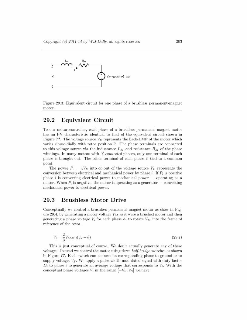
Copyright (c) 2011-14 by W.J Dally, all rights reserved 203
LM RM
VE=KM sin iVi
+
-
ii
+
Figure 29.3: Equivalent circuit for one phase of a brushless permanent-magnetmotor.
29.2 Equivalent Circuit
To our motor controller, each phase of a brushless permanent magnet motorhas an I-V characteristic identical to that of the equivalent circuit shown inFigure ??. The voltage source VE represents the back-EMF of the motor whichvaries sinusoidially with rotor position θ. The phase terminals are connectedto this voltage source via the inductance LM and resistance RM of the phasewindings. In many motors with Y-connected phases, only one terminal of eachphase is brought out. The other terminal of each phase is tied to a commonpoint.
The power Pi = iiVE into or out of the voltage source VE represents theconversion between electrical and mechanical power by phase i. If Pi is positivephase i is converting electrical power to mechanical power — operating as amotor. When Pi is negative, the motor is operating as a generator — convertingmechanical power to electrical power.
29.3 Brushless Motor Drive
Conceptually we control a brushless permanent magnet motor as show in Fig-ure 29.4, by generating a motor voltage VM as it were a brushed motor and thengenerating a phase voltage Vi for each phase φi to rotate VM into the frame ofreference of the rotor.
Vi =23VMsin(ψi − θ) (29.7)
This is just conceptual of course. We don’t actually generate any of thesevoltages. Instead we control the motor using three half-bridge switches as shownin Figure ??. Each switch can connect its corresponding phase to ground or tosupply voltage, VS . We apply a pulse-width modulated signal with duty factorDi to phase i to generate an average voltage that corresponds to Vi. With theconceptual phase voltages Vi in the range [−VS , VS ] we have:

204 Green Electronics
Brushed PMMotor
ControllerInverter
VM
V1
V2
V3
BrushlessPM Motor
Figure 29.4: We conceptually divide a brushless motor controller into two blocks.The first block computes the motor drive voltage VM that would be required todrive an equivalent brushless motor. The second block generates phase voltagesV1, V2, and V3 to rotate VM to θ + π/2 for motor position θ.
1 2 3
VS
+
-
s1
s1
s2
s2
s3
s3
Figure 29.5: A three-phase motor driver consists of three half bridges that gener-ate the three phase voltages. For each phase φi switch si generates a pulse-widthmodulated signal with duty factor Di and mean value DiV1.

Copyright (c) 2011-14 by W.J Dally, all rights reserved 205
Di = 0.5(1 +Vi
VS) (29.8)
= 0.5(1 +VMsin(ψi − θ)
VS) (29.9)
(29.10)
This converts each conceptual voltages Vi to an actual average phase voltage ofVi according to
Vi = 0.5(VS + Vi) (29.11)
That is Vi = 0 maps to Vi = 0.5VS , Vi = VS maps to Vi = VS , and Vi = −VS
maps to Vi = 0.Because the three phases are distributed evenly around the unit circle the
average of the three phase voltages is always VS/2 and this is the voltage at thecommon point at the center of the three windings.
In some cases it is desirable to minimize the phase voltages. We can accom-plish this by subtracting the minimum duty factor from all of the duty factors.This effectively lowers the common mode voltage so that one phase is always atground potential. The modified duty factors D′i are calculated as
Dmin =n
mini=1
(Di)
D′i = Di −Dmin (29.12)
This transformation does result in an AC component on the common node ofthe motor. If this is objectinable the minimum duty factor of any phase overan entire cycle can be subtracted from each phases duty factor instead of theinstantaneous minimum.
29.4 Hard Electronic Commutation
[to be written]
29.5 Excercises

206 Green Electronics

Chapter 30
AC Induction Motors
AC induction motors are among the most common motors in use for higher-output applications. They have attractive power for a given weight and sizeand do not require rare-earth magnets. They tend to be slightly less efficientthan a comparable brushless permanent magnet motor because they introducerotor condution losses.
30.1 Motor Geometry
As shown in Figure 30.1 an AC induction motor has a stator identical to abrushless permanent magnet motor but substitutes a sqirrel cage rotor of con-ductive bars that are shorted together at both ends for the permanent magnetrotor. The motor can be constructed either with coils wound on salient poles asshown in Figure 30.1 or with a stator consisting of coils surrounding the entirerotor as showni n Figure 30.2. As in the brushless motor the stator is drivenwith a three-phase sinusoidal signal to produce a rotating magnetic field withfrequency ωs. If the rotor is turning with frequency ωr, each rotor bar sees amagnetic field at the difference freqency ωd = ωs −ωr. This changing magneticfield induces a voltage across the rotor bars and this voltage in turn causes cur-rent to flow in the bars. This rotor current interacts with the magnetic field togenerate torque.
In effect the coupling between the stator and the rotor in an induction motoracts as a transformer (Section 10.1) generating voltage and current in the rotorin response to voltage applied to the stator. The rotor current then generates amotor torque and, if the rotor is moving, a back EMF.
30.2 Induction Motor Operation
Operation of the induction motor can be understood in terms of rotating voltage,current, and fluxes as shown in Figure ??. Here we represent AC quantities inthe two-dimensional plane as an amplitude and a phase. For example, if we
207
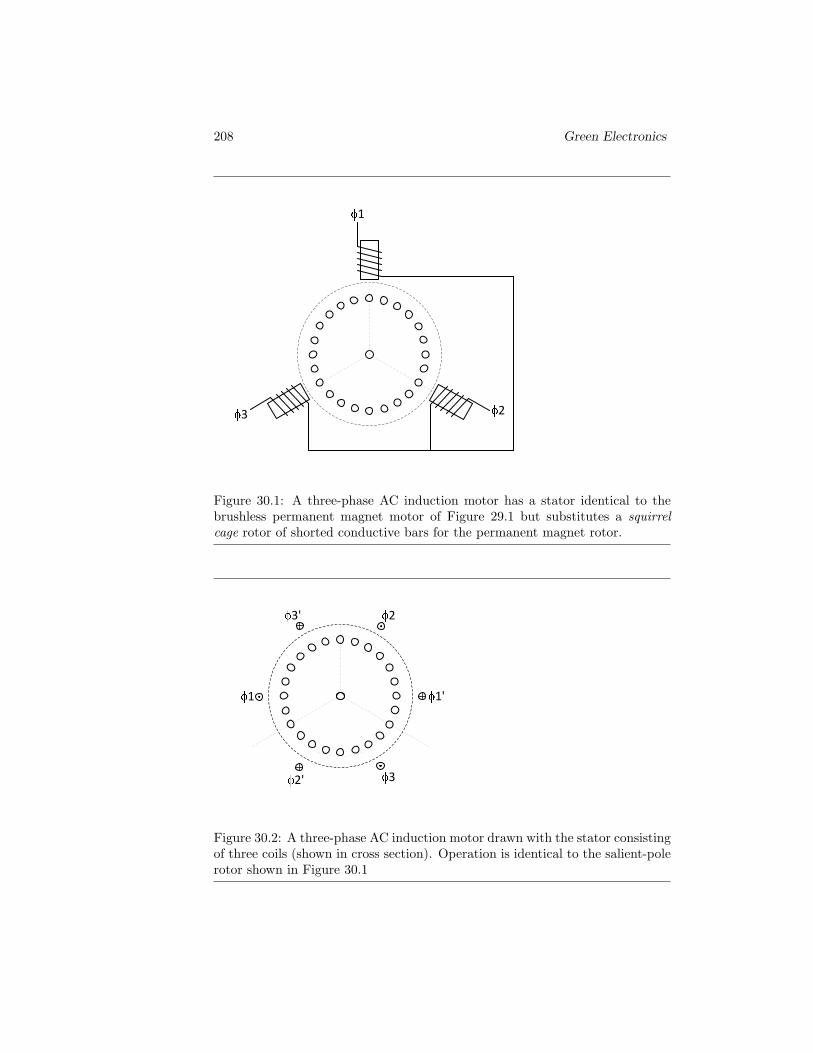
208 Green Electronics
1
23
Figure 30.1: A three-phase AC induction motor has a stator identical to thebrushless permanent magnet motor of Figure 29.1 but substitutes a squirrelcage rotor of shorted conductive bars for the permanent magnet rotor.
1
2
3
1'
2'
3'
Figure 30.2: A three-phase AC induction motor drawn with the stator consistingof three coils (shown in cross section). Operation is identical to the salient-polerotor shown in Figure 30.1
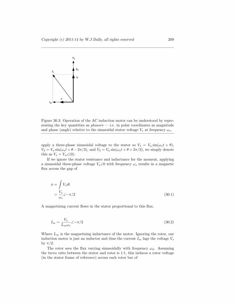
Copyright (c) 2011-14 by W.J Dally, all rights reserved 209
VS
IM
VR
IR
IS
Figure 30.3: Operation of the AC induction motor can be understood by repre-senting the key quantities as phasors — i.e. in polar coordinates as magnitudeand phase (angle) relative to the sinusoidal stator voltage Vs at frequency ωs.
apply a three-phase sinusoidal voltage to the stator so V1 = Va sin(ωst + θ),V2 = Va sin(ωst+ θ− 2π/3), and V3 = Va sin(ωst+ θ+ 2π/3), we simply denotethis as Vs = Va∠(0).
If we ignore the stator resistance and inductance for the moment, applyinga sinusoidal three-phase voltage Vs∠0 with frequency ωs results in a magneticflux across the gap of
φ =∫Vsdt
=Vs
ωs∠−π/2 (30.1)
A magnetizing current flows in the stator proportional to this flux.
Im =Vs
Lmωs∠−π/2 (30.2)
Where Lm is the magnetizing inductance of the motor. Ignoring the rotor, ourinduction motor is just an inductor and thus the current Im lags the voltage Vs
by π/2.The rotor sees the flux varying sinusoidally with frequency ωd. Assuming
the turns ratio between the stator and rotor is 1:1, this induces a rotor voltage(in the stator frame of reference) across each rotor bar of

210 Green Electronics
Vr =dφ
dt
=Vsωd
ωs∠0
= σVs∠0. (30.3)
As expected for a transformer, our rotor voltage is in-phase with the statorvoltage. Unlike a stationary transformer our rotor voltage is scaled by σ = ωd
ωs
a quantity referred to as the slip of the motor1.If the rotor bars have an aggregate resistance of Rr the rotor voltage Vr
causes a rotor current with value
Ir =Vr
Rr∠0
=σVs
Rr∠0 (30.4)
In practice rotor inductance will cause Ir to slightly lag Vs. We ignore thateffect for now.
Because of the scaling of rotor voltage by σ, the rotor resistance reflectedback to the stator — i.e. the rotor resistance seen by Vs is
R′r =Rr
σ
=ωsRr
ωd(30.5)
When there is no slip, σ = 0, R′r is infinite and no rotor current flows. Whenthe rotor is locked σ = 1 and R′r = Rr. For other cases of positive slip R′r > Rr.If ωr > ωs, we have a negative resistance, R′r < −Rr. In this case the motor isoperating as a generator.
The overall stator current is the vector sum of the magnetizing current andthe rotor current reflected to the stator.
Is = Im + Ir (30.6)
As shown in Figure 30.3, This stator current is at a negative angle intermediatebetween 0 and −π/2.
Current Ir interacts with the magnetic field to produce a torque
1Many texts use the variable s to represent slip. We use σ here to avoid confusion withlaplace transforms.
Copyright (c) 2011-14 by W.J Dally, all rights reserved 211
τ = Irφ
=σV 2
s
ωsRr
=V 2
s ωd
ω2sRr
(30.7)
Torque increases quadratically with Vs since both the φ and Ir depend linearlyon Vs. Torque decreases with increased stator frequency ωs because φ decreaseswith frequency. Note that τ is a DC value, not an AC signal, so it has no phase.
The output power delivered by the motor to its shaft (or received from theshaft if negative) is
PO = τωr
= Irφωr
= IrVsωr
ωs
= I2rRr
ωr
ωd
= I2rRr
1− σ
σ(30.8)
We rewrite PO in the form I2R to facilitate development of our equivalent circuitin the next section.
30.3 Equivalent Circuit
The behavior of an AC induction motor can be analyzed using the equivalentcircuit of Figure 30.4. The circuit represents one of the three phases of themotor.
Voltage Vs is applied to one stator phase. Stator current Is passes throughthe stator winding resistance Rs and leakage inductance Ls before splitting.Magnetizing current (30.2) passes through magnetizing inductance Lm. Thereflected rotor current passes through the leakage inductance of the rotor Lr
and the scaled rotor bar resistance RR/σ which we have split into loss andoutput components. The dotted line represents the air-gap between the statorand the rotor.
From (30.4) we see that the effective rotor resistance seen by Vs is R′r =Rr/σ. We split this scaled rotor resistance into two components to separatethe component of the resistance that represents conduction losses in the rotorRrl from the component that represents the output power produced by themotor Rro. From (30.8) we see that the motor power is equivalent to the powerdissipated by passing the rotor current through a resistor with value:

212 Green Electronics
LS RS
VS
+
-
iS
LM
LR
RR
RR1-
iM
iR
Air Gap
stat
or
roto
rFigure 30.4: Equivalent circuit for one phase of an AC induction motor. Thestator voltage induces a magnetizing current Im (30.2) across magnetizing in-ductance Lm and a rotor current (reflected to the stator) Ir (30.4) across ascaled rotor resistance Rr. We add stator resistance Rs and stator and rotorleakage inductances Ls and Lr to complete our model.
Rro =(ωr
ωd
)Rr
=(
1− σ
σ
)Rr (30.9)
The remaining portion of R′r is:
Rrl = R′r −Rro
=(
1σ− 1− σ
σ
)Rr
= Rr (30.10)
This is as expected since the power dissipated by Ir flowing through the actualrotor resistance Rr is in fact dissipated in the resistance of the rotor.
30.4 Induction Motor Control
The drive used to control a three-phase (or N-phase) induction motor is identicalto the drive used for a brushless permanent magnet: a three-phase inverter. Asshown in Figure 29.5, a half-bridge driven with a PWM signal generates anappropriate average voltage, sin(ωst− ψi), for each phase φi.

Copyright (c) 2011-14 by W.J Dally, all rights reserved 213
While the drive itself is identical, the algorithm used to control the drivediffers significantly between the two motors. For a brushless motor, we deter-mine the rotor position θ and apply a current at θ− π/2 to generate torque. Incontrast, we don’t care about the position of an induction motor. Instead wedetermine rotor velocity ωr and determine the optimum combination of voltageVs and stator frequeny ωs to apply the desired torque τ per equation (30.7). Ofthe many possible solutions, one is chosen to optimize a figure of merit subjectto constraints.
In most cases the figure of merit we choose to optimize is efficiency ν =Po/Pi. Ignoring stator losses, we can calculate the efficiency of our motor fromthe resistive voltage divider of Figure 30.4:
ν =Rro
Rro +Rrl
=ωr
ωd
ωr
ωd+ 1
=ωr
ωr + ωd
=ωr
ωs
= 1− σ (30.11)
We see that efficiency is determined entirely by slip. When σ = 1 (locked rotor)there is no output power and ν = 0. When σ = 0 (synchronous operation) thereis no rotor current and hence no rotor losses — unfortunately there is also notorque. Slip is required to generate torque. As slip increases we get more torquefor a given Vs but we also operate less efficiently.
A typical motor controller will be subject to the constraints:
Vs ≤ Vmax (30.12)Is ≤ Imax (30.13)
We can think of the constraints as establishing a feasible region in the ωs, Vs
plane (Figure 30.5). The voltage constraint (30.13) specifies that all possiblesolutions must be below the Vmax line in this plane. The current constraint(30.13) applied to the magnetizing current (30.2) specifies that all solutions beto the right of an Imax diagonal:
ωs ≥Vs
LmImax(30.14)
These two constraints are shown as thick dotted lines in the figure. The pointwhere the two constraints intersect occurs at
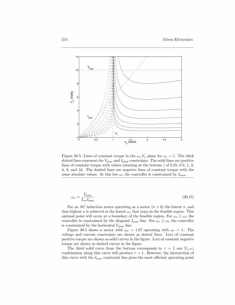
214 Green Electronics
0 0.5 1 1.5 2 2.5 30
2
4
6
8
10
12
Vmax
Imax
tr
ts (rad/s)
V s (Vol
ts)
Figure 30.5: Lines of constant torque in the ωs,Vs plane for ωr = 1. The thickdotted lines represent the Vmax and Imax constraints. The solid lines are positivelines of constant torque with values (starting at the bottom ) of 0.25, 0.5, 1, 2,4, 8, and 16. The dashed lines are negative lines of constant torque with thesame absolute values. At this low ωr the controller is constrained by Imax.
ωx =Vmax
LmImax(30.15)
For an AC induction motor operating as a motor (σ > 0) the lowest σ, andthus highest ν is achieved at the lowest ωs that stays in the feasible region. Thisoptimal point will occur at a boundary of the feasible region. For ωs ≤ ωx thecontroller is constrained by the diagonal Imax line. For ωs ≥ ωx the controlleris constrained by the horizontal Vmax line.
Figure 30.5 shows a motor with ωx = 1.67 operating with ωr = 1. Thevoltage and current constraints are shown as dotted lines. Loci of constantpositive torque are shown as solid curves in the figure. Loci of constant negativetorque are shown as dashed curves in the figure.
The third solid curve from the bottom corresponds to τ = 1 any Vs, ωs
combination along this curve will produce τ = 1. However, the intersection ofthis curve with the Imax constraint line gives the most efficient operating point
Copyright (c) 2011-14 by W.J Dally, all rights reserved 215
for τ = 1. We can calculate this current-constrained operating point, Vsc, ωsc
as:
Vsc = LmImaxωsc (30.16)
τ =ω2
scL2mI
2maxωdc
ω2scRr
=L2
mI2maxωdc
Rr
ωdc =τRr
L2mI
2max
ωsc =τRr
L2mI
2max
+ ωr (30.17)
Vsc =τRr
LmImax+ ωrLmImax (30.18)
At this operating point we have:
σ =τRr
τRr + ωrI2maxL
2m
(30.19)
ν =ωrI
2maxL
2m
τRr + ωrI2maxL
2m
(30.20)
Figure 30.6 shows the case where ωs > ωx and the controller is constrained byvoltage rather than current. In this case ωr = 3 and the constant-torque curvesare all constrained by the Vmax line. To solve for the point of intersection wesubstitute (30.12) into (30.7) to give a quadratic equaiton that can be solvedfor the voltage-constrained operating frequency, ωsv.
τ =V 2
maxωdv
ω2svRr
0 = τRrω2sv − V 2
maxωsv + V 2maxωr
ωsv =V 2
max −√V 4
max − 4τRrV 2maxωr
2τRr(30.21)
Solving (30.21) for τ = 1 for example gives ωsv = 3.1. We pick the smaller ofthe two solutions to the quadratic equation because it results in less slip. Theother solution represents the point where the constant-torque curve rises aboveVmax at very high frequency. This point is almost visible only for the τ = 8curve at ωs = 7.5.
In practice the controller finds both voltage-constrained and current-constrainedoperating points and and selects the point with the lower Vs and the higher ωs
as being the most constrained.

216 Green Electronics
0 1 2 3 4 5 6 70
2
4
6
8
10
12
Vmax
Imax
tr
ts (rad/s)
V s (Vol
ts)
Figure 30.6: Lines of constant torque in the ωs,Vs plane for ωr = 3. At thishigher speed the controller is entirely constrained by Vmax and the torque valueof +16 is not achievable.

Copyright (c) 2011-14 by W.J Dally, all rights reserved 217
Figures 30.5 and 30.6 also show curves of constant negative torque — asdashed lines. When braking (producing negative torque) the controller com-putes operating points in the same manner as for positive torque. Current-constrained and voltage constrained operating points are calculated using (??)and (30.21) with negative values of torque. For negative torque the constrainedoperating point with the lower ωs is chosen as being the most constrained.
30.5 Exercises

218 Green Electronics
Part Part IV - ControlRevisiting Buck controlPD controllerCurrent-mode controlEnergy-based controlCharge based controlA hybrid controllerBode plotsPhase margin and stabilityIntegral windupPredictive controlModel-based controlSensing and estimation

Copyright (c) 2011-14 by W.J Dally, all rights reserved 219
Part V - Practical DesignAn example buck converterPower factor correctionAn inverter

220 Green Electronics
Part VI - Efficient DesignLossesConduction lossesSwitching lossesGate lossesLeakage inductance losses (in flyback)Soft switchingQuasi-square waveActive clampIsolated sensing

Chapter 31
Soft Switching
The switching losses of a converter can be largely eliminated by changing thestate of the switching elements (typically FETs or IGBTs) only when they haveeither zero voltage across them or zero current through them. This is calledzero voltage switching (ZVS) or zero current switching (ZCS). Collectively thetwo techniques are called soft switching. In contrast the conventional convert-ers described in Chapters 2 to 12 are hard-switching converters because theychange the state of switches with both non-zero current and voltage — leadingto switching losses.
In this chapter we introduce soft switching by examining a quasi-square-wave(QSW) buck converter, one of the simplest ZVS converters. This converter isjust a conventional buck converter with one capacitor added to slow the voltagetransient. The control of the QSW converter, however, differs substantiallyfrom the control of a conventional buck and requires a gate drive with variablefrequency.
In subsequent chapters we will explore quasi-resonant converters and con-verters employing an active clamp.
31.1 The Quasi-Square-Wave Converter
Figure 31.1 shows a schematic diagram of a QSW buck converter. The circuit isidentical to the buck converter of Figure 2.3 except for the addition of capacitorCX to slow the voltage transitions on node X, the drain of M2.
The main difference between the QSW converter and the hard-switched buckis not the topology but rather how it is controlled and the very high inductorripple currents that result. To turn M1 and M2 on ZVS, the QSW converteruses current in the inductor to charge and discharge CX so there is no voltageacross each FET when it is switched on. To charge CX to VS before turningon M1 requires the current in L to be negative. To keep the average inductorcurrent equal to the load current the peak current must be more than twice theload current.
221

222 Green Electronics
L
iL
VS
+
-
vC Load
+
-
C iLoadM2L
M1H
CX
D1
D2
Figure 31.1: A quasi-square-wave (QSW) buck converter adds capacitor CX toa conventional buck converter to slow the voltage swing on the drain of M2 tofacilitate ZVS of both switches.
Parameter Value Units DescriptionC 100 µF filter capacitorL 10 µH inductorCX 47 nF drain capacitorVS 100 V supply voltageVC 50 V output voltageIL 5 A load current
Table 31.1: Parameters and component values for the QSW buck simulation ofFigure 31.2.

Copyright (c) 2011-14 by W.J Dally, all rights reserved 223
0 1 2 3 4 5 6 7−5
0
5
10
i L (A)
0 1 2 3 4 5 6 7
0
20
40
60
80
100
v X (V)
Time (µs)
Figure 31.2: Waveforms showing operation of the QSW buck converter of Fig-ure 31.1 with the parameters of Table 31.1. The inductor current (top panel)goes negative to store energy to charge CX . The voltage on CX (bottom panel)consists of segments of sine waves during transients.
Figure 31.2 shows inductor current and voltage across capacitor CX for onecycle of operation for the QSW converter of Figure 31.1 with the parametersshown in Table 31.1. We divide the cycle into four periods that are delimitedby switching either M1 or M2 on or off.
Initially M1 is on and the inductor current ramps from 0 to a thresholdvalue of 11A. When this threshold ihigh is reached, M1 turns off ZVS at 2.23µs.Capacitor CX slows the fall of node X so that very little voltage develops acrossM1 before its current has gone to zero. The fall time of node X is 420ns. FromFigure 17.2 we saw a typical FET can be switched off in 10-20ns. Thus, at most5V will develop across M1 while its current ramps down.
During the 420ns fall time of node X both switches are off. Capacitor CX
is discharged by the inductor current which peaks at 11.5A giving a slew rateof 24V/µs. This slew rate is determined by the value of CX which is chosenlarge enough to make the loss of turning M1 off negligible. During the fall ofnode X both inductor current and node voltage vary sinusoidally1 as the tank
1The node voltage looks like a striaght line but it is in fact part of a sine wave.

224 Green Electronics
circuit formed by L and CX oscillates. The voltage passes through the peakof the sine wave while the current passes through the portion of the sine wavewith the steepest descent.
When node X falls through 0 the body diode of M2 turns on clamping VX
a diode drop below ground. At this point M2 is turned on ZVS. With M2 onand node X at 0 V current in the inductor ramps down from 11A at 2.65µs toa threshold value of ilow = 0A at 4.86µs. When ilow is reached M2 is turned offZVS. As with the turn-off of M1, capacitor CX keeps the voltage across M2 nearzero while its current ramps down. In this case, because the inductor current isso low, the voltage change during hte turn-off of M2 is negligible.
With both switches off again, the tank circuit formed by L and CX resumesoscillation — but this time with the inductor feeding current into nodeX causingit to rise. During this period both waveforms are again sinusoidal with thecurrent following the bottom of the sine wave and the voltage the rising segment.With a much lower starting current 1A vs 11A the rise time of node X is muchslower than the fall time — taking 1.7µs to slew from 0 to VS . When vX reachsvS the body diode of M1 clamps it at this value. At this point M2 switches onZVS and the cycle has completed.
During the fall time from 2.23− 2.65µs and the rise time from 4.86− 6.86µsboth switches are off and the tank circuit formed by CX and L oscillates. Thefrequency of this oscillation is fX = 1
2π√
LCX= 232kHz. This frequency is
unrelated to frequency of the switching cycle, which in this case is 148kHz. Tomake the figures easier to understand we have set fX unusually low. In a typicalconverter it would be many times this value.
For a fixed value of CX , this rise time could be made faster by setting alower (more negative) value of ilow. However, we typically want to keep ilow tothe highest value that provides sufficient current to drive node X to VS . Thisvalue is given by:
ilow = − (VS − 2VC)
√CX
L(31.1)
Setting ilow below this point increases current ripple which in turn leads toincreased conduction and core losses.
If ilow is a little too high the inductor current will cross zero before vX
reaches vS . This case is illustrated in Figure 31.3. Here we have set vC to 45V,so starting from zero inductor current the LC tank rings vX up to 90V (twicethe initial voltage). The FET switches on when iL passes through zero and pullsvX up the remaining 10V. While this is not exactly ZVS operation, switchingwith 10V across the terminals of M1 requires much less energy than switchingwith 100V across the terminals. We can avoid this issue altogether by settingilow sufficiently low.
The frequency of a QSW converter varies with average current. The lowerthe current the higher the switching frequency. Figure 31.4 illustrates converteroperation with i = 0.7A. The cycle time here is just 4.7µs compared to 6.9µs inFigure 31.2.

Copyright (c) 2011-14 by W.J Dally, all rights reserved 225
0 1 2 3 4 5 6 7 8−5
0
5
10
15
i L (A)
0 1 2 3 4 5 6 7 8
0
20
40
60
80
100
v X (V)
Time (µs)
Figure 31.3: Waveforms showing operation of the QSW buck converter of Fig-ure 31.1 with the parameters of Table 31.1 but with vC = 45V. In this case iLcrosses zero before vX reaches vS . We turn on M1 at this point and it pulls vX
up the last 10V.
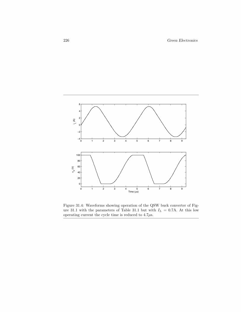
226 Green Electronics
0 1 2 3 4 5 6 7 8 9−4
−2
0
2
4
6
i L (A)
0 1 2 3 4 5 6 7 8 9
0
20
40
60
80
100
v X (V)
Time (µs)
Figure 31.4: Waveforms showing operation of the QSW buck converter of Fig-ure 31.1 with the parameters of Table 31.1 but with IL = 0.7A. At this lowoperating current the cycle time is reduced to 4.7µs.

Copyright (c) 2011-14 by W.J Dally, all rights reserved 227
0 1 2 3 4 5 6 7 8−4
−2
0
2
4
6
i L (A)
0 1 2 3 4 5 6 7 8
0
20
40
60
80
100
v X (V)
Time (µs)
Figure 31.5: Waveforms showing operation of the QSW buck converter of Fig-ure 31.1 with the same parameters as in Figure 31.4. To increase the cycletime the controller skips an entire cycle of the LC tank before turning on M1
stretching the cycle time to 9.1µs.
To avoid excessive switching at low currents the QSW converter can skipone or more cycles of the LC tank before turning on M1. Skipping one cycle isillustrated in Figure 31.5. When M2 turns off at 2.6µs the LC tank is allowedto oscillate not for a quarter cycle (as in Figure 31.2-Figure 31.4) but for 1.25cycles. The oscillation is halted when M1 turns on the second time vX reachesvS .
31.2 Control of the Quasi-Square-Wave Converter
As described above, the four events in the switching cycle are triggered by iland vX reaching thresholds. The off events are triggered by current thresholdsand the on events are triggered by voltage thresholds.
M1 Off: When iL > ihigh.
M2 On: When vX < 0.
228 Green Electronics
M2 Off: When iL < ilow.
M1 On: When vX > VS or iL > 0.
We add the or condition to the M1 on trigger to handle cases where the inductorruns out of current before vX reaches vS .
From these trigger conditions we see that the control variables are the twocurrent thresholds, and if keep ilow near its maximum value to minimize losses,we have a single control variable ihigh. Thus we control a QSW converter bysetting threshold ihigh. This in turn determines the average current over thecycle i which integrates on C to determine the output voltage.
The transfer function of the system is:
vc(s)ihigh(s)
=K
Cs(31.2)
where K is the gain constant relating ihigh to i.Applying a PI controller with transfer function P + Q/s gives open- and
closed-loop transfer functions:
G(s) =KPs+KQ
Cs2(31.3)
H(s) =KPC s+ KQ
C
s2 + KPC s+ KQ
C
(31.4)
So we have
ω =
√KQ
C(31.5)
ζ =KP
2ωC(31.6)
Q =ω2C
K(31.7)
P =2CζωK
(31.8)
Figure 31.6 shows a simulation of a QSW converter using a PI controller withω chosen to be 6.28 × 10³. The waveforms show the response of the controllerto two shifts in target voltage. The controller goes non-linear during bothtransients with ihigh (middle panel) being clamped to its low limit of 0 A duringthe downward transient and to 20A during the upward transient. There issome integral wind-up in the controller during these periods where the outputis saturated.
The waveforms show how cycle time varies with current. As ihigh varies from0 to 20A, tcy varies by more than 2:1 from a minimum of 4.3µs when the currentis 0A to 10.5µs when ihigh is set to 20A.

Copyright (c) 2011-14 by W.J Dally, all rights reserved 229
0 200 400 600 800 1000 1200
45
50
55
v C (V
)
0 200 400 600 800 1000 1200
05
101520
i high
(A)
0 200 400 600 800 1000 1200
4
6
8
10
12
t cy (µ
s)
t (µs)
Figure 31.6: Simulated waveforms of a QSW buck converter with a PI controller.The target voltage is changed to 45V at 274µs and to 55V at 707µs.

230 Green Electronics
31.3 Exercises
evaluate switching lossplay with values of CX
design and simulate a QSW boost converterexplore effects on comonent values and ratings