˘ 9 ˆ ˘ P FP2 Normally-off 4H-SiC VJFET Design ...
4
9P FP 2 Normally-off 4H-SiC VJFET Design, Fabrication and Characterization L. Fursin 1,2 , X. Li 1,2 , and J. H. Zhao 1 1 SiCLAB, ECE Dept., Rutgers University, 94 Brett Road, Piscataway, NJ 08854, USA 2 United Silicon Carbide, Inc., 100 Jersey Ave, Bldg. A, New Brunswick, NJ 08901, USA Keywords: 4H-SiC, power junction field-effect transistor, JFET, high voltage. Abstract. This paper reports the design, fabrication and characterization of a double-gated, normally-off 4H-SiC VJFETs with implanted vertical channel, which eliminates the need of epitaxial re-growth in the middle of the device fabrication. A normally-off VJFET, which is based on a 15μm n-type drift layer doped to n=5.7x10 15 cm -3 , is demonstrated with a blocking voltage (V B ) of 1,530V with a leakage current of 15mA. The specific on-resistance (R SP_ON ) is found to be 17.5 mΩcm 2 at J D =100A/cm 2 and V G =3.5V. The VJFET conducts a drain current of 1.13A (227A/cm 2 ) at V G =3.5V and V D =5V with a corresponding gate current of 16mA, resulting in an I D /I G ratio of 70. VJFETs with different lateral JFET channel opening dimensions have been designed and fabricated. Detailed design, fabrication and characterization results of the VJFETs are reported, including the DC I-V relations, the effects of LJFET channel opening dimensions, the specific on-resistance, and the temperature-dependent performance. Introduction 4H-SiC VJFETs, being free of gate-oxide related problems, have been investigated by a number of groups for possible high power and high temperature applications [1-5]. To make VJFETs normally-off, one can use a buried p layer to form a low voltage, normally-off lateral JFET to control a monolithically merged normally-on vertical JFET formed by ion implantation without epitaxial re-growth [1,2] or by epitaxial re-growth [3,4]. The best normally-off VJFET employing epitaxial re-growth has a V B of 5.3kV and an R SP_ON of 69 m cm 2 at J D ~15A/cm 2 and V G =+5V, corresponding to a V B 2 /R SP_ON of 407 MW/cm 2 [4]. In this paper, we report the design and development of processing technology for the demonstration of a double-gated, normally-off 4H- SiC VJFET with V B =1,530V and R SP_ON =17.5m cm 2 at a high current density (J D ) of 100A/cm 2 , corresponding to V B 2 /R SP_ON of 134 MW/cm 2 , which compares very favorably with the value of 125MW/cm 2 for the best 4H- SiC MOSFET of a similar blocking voltage. Device Design, Fabrication, and Characterization The cross sectional view of the VJFET is shown in Fig.1, where the n- drift layer is 15μm and doped to Fig.1 Cross sectional view of the VJFET.
Transcript of ˘ 9 ˆ ˘ P FP2 Normally-off 4H-SiC VJFET Design ...

9P FP2 Normally-off 4H-SiC VJFETDesign, Fabrication and Characterization
L. Fursin1,2, X. Li1,2, and J. H. Zhao1
1 SiCLAB, ECE Dept., Rutgers University, 94 Brett Road, Piscataway, NJ 08854, USA2 United Silicon Carbide, Inc., 100 Jersey Ave, Bldg. A, New Brunswick, NJ 08901, USA
Keywords: 4H-SiC, power junction field-effect transistor, JFET, high voltage.
Abstract. This paper reports the design, fabrication and characterization of a double-gated,normally-off 4H-SiC VJFETs with implanted vertical channel, which eliminates the need ofepitaxial re-growth in the middle of the device fabrication. A normally-off VJFET, which is basedon a 15µm n-type drift layer doped to n=5.7x1015cm-3, is demonstrated with a blocking voltage (VB)of 1,530V with a leakage current of 15mA. The specific on-resistance (RSP_ON) is found to be 17.5mΩcm2 at JD=100A/cm2 and VG=3.5V. The VJFET conducts a drain current of 1.13A (227A/cm2)at VG=3.5V and VD=5V with a corresponding gate current of 16mA, resulting in an ID/IG ratio of 70.VJFETs with different lateral JFET channel opening dimensions have been designed and fabricated.Detailed design, fabrication and characterization results of the VJFETs are reported, including theDC I-V relations, the effects of LJFET channel opening dimensions, the specific on-resistance, andthe temperature-dependent performance.
Introduction
4H-SiC VJFETs, being free of gate-oxide related problems, have been investigated by a number ofgroups for possible high power and high temperature applications [1-5]. To make VJFETsnormally-off, one can use a buried p layer to form a low voltage, normally-off lateral JFET tocontrol a monolithically merged normally-on vertical JFET formed by ion implantation withoutepitaxial re-growth [1,2] or by epitaxial re-growth [3,4]. The best normally-off VJFET employingepitaxial re-growth has a VB of 5.3kV and an RSP_ON of 69 m cm2 at JD~15A/cm2 and VG=+5V,corresponding to a VB
2/RSP_ON of 407 MW/cm2 [4]. In this paper, we report the design anddevelopment of processing technology for the demonstration of a double-gated, normally-off 4H-
SiC VJFET with VB=1,530Vand RSP_ON=17.5m cm2 at ahigh current density (JD) of100A/cm2, corresponding toVB
2/RSP_ON of 134 MW/cm2,which compares veryfavorably with the value of125MW/cm2 for the best 4H-SiC MOSFET of a similarblocking voltage.
Device Design, Fabrication,and Characterization
The cross sectional view ofthe VJFET is shown in Fig.1,where the n- drift layer is15µm and doped to
Fig.1 Cross sectional view of the VJFET.
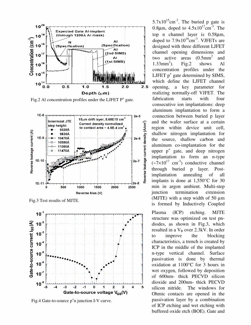
5.7x1015cm-3. The buried p gate is0.8µm, doped to 4.5x1017cm-3. Thetop n channel layer is 0.58µm,doped to 7.9x1016cm-3. VJFETs aredesigned with three different LJFETchannel opening dimensions andtwo active areas (0.5mm2 and1.33mm2). Fig.2 shows Alconcentration profiles under theLJFET p+ gate determined by SIMS,which define the LJFET channelopening, a key parameter forrealizing normally-off VJFET. Thefabrication starts with fourconsecutive ion implantations: deepaluminum implantation to form aconnection between buried p layerand the wafer surface at a certainregion within device unit cell,shallow nitrogen implantation forthe source, shallow carbon andaluminum co-implantation for theupper p+ gate, and deep nitrogenimplantation to form an n-type(~7×1017 cm-3) conductive channelthrough buried p layer. Post-implantation annealing of allimplants is done at 1,550°C for 30min in argon ambient. Multi-stepjunction termination extension(MJTE) with a step width of 50 µmis formed by Inductively Coupled
Plasma (ICP) etching. MJTEstructure was optimized on test pn-diodes, as shown in Fig.3, whichresulted in a VB over 2.3kV. In orderto improve the blockingcharacteristics, a trench is created byICP in the middle of the implantedn-type vertical channel. Surfacepassivation is done by thermaloxidation at 1100°C for 3 hours inwet oxygen, followed by depositionof 600nm- thick PECVD silicondioxide and 200nm- thick PECVDsilicon nitride. The windows forOhmic contacts are opened in thepassivation layer by a combinationof ICP etching and wet etching withbuffered oxide etch (BOE). Gate and
Fig.2 Al concentration profiles under the LJFET P+ gate.
Fig.3 Test results of MJTE.
Fig.4 Gate-to-source p+n junction I-V curve.

source Ohmic contacts are formed withsputtered Ni/TiW (20/80 nm). Draincontact is formed with sputtered Al/Ni(20/300 nm) on the substrate. Allcontacts were annealed simultaneouslyat 1,050°C for 10 min. Ti/Au is used toform overlay buses and bonding pads.Total overlay thickness is 1.7 µm forthe source and 0.8 µm for the gate.Arrays of the implanted upper p+ gatesare connected to metallized gate busesat selected locations, which results in alower voltage drop across the p+njunction gate than the externallyapplied gate voltage. Fig.4 shows thegate-to-source p+n junction I-Vcharacteristics and Fig.5 presents thegate-to-drain p-n I-V curve for a VJFETwith wide LJFET channel opening. Theresults confirm the realization of a goodp+n gate junction based on high doseimplantation of C plus Al. Fig.6 showsthe DC I-V & J-V characteristics of asmall VJFET (active area 0.5mm2) withwide LJFET channel opening. Forwardcurrent is characterized at both roomtemperature and 150°C for the same setof gate voltages. At room temperature,the leakage current is 15mA atVB=1,530V. Based on Fig.6, it is seenthat, at VG=3.5V, the current density JD
is 50 and 100 A/cm2 at VD=0.84V and1.75V, respectively, corresponding to anRSP_ON of 16.8 and 17.5 m cm2,respectively. At room temperature, thegate currents are 94µA, 2.7mA, 16mAand 43mA for VG=2.5, 3, 3.5, and 4V,respectively. RSP_ON of 16.8 and 17.5
m cm2 and VB of 1,530V correspond to a figure-of-merit (FOM) of VB2/ RSP_ON of 139 and 134
MW/cm2, respectively. As a reference, the best 4H-SiC UMOSFET with a similar voltage rating hasa VB
2/ RSP_ON of ~125 MW/cm2 [6]. Fig. 7 shows the DC I-V & J-V characteristics of a largeVJFET (active area of 1.33mm2) with wide LJFET channel opening. For 3.5 V gate bias, thespecific on-resistance corresponding to JD= 50 and 100A/cm2, is 21.6 and 25.8 m cm2,respectively. Fig. 8 shows the DC I-V & J-V characteristics of a small VJFET with narrow LJFETchannel opening. As could be seen by comparing to Figs. 6 and 7, the VJFET with narrow LJFETchannel opening requires higher gate bias for device to conduct appreciable amount of current (1.5Vcompared to 1.0V for wide LJFET channel opening). For 3.5 V gate bias, the specific on-resistancecorresponding to JD of 50 and 100 A/cm2, is 18.8 and 21.4 m cm2, respectively. At roomtemperature, the gate currents are 270µA, 18mA, 75mA and >100mA for VG=2.5, 3, 3.5, and 4V,respectively. As could be noticed, devices with wider LJFET channel opening (lower dose andshallower p+ Al+C co-implantation) demonstrate lower gate current under same gate-to-source and
Fig.5 Gate-to-drain p+n junction I-V curve.
Fig.6 I-V & J-V characteristics of a small VJFET (activearea of 0.5mm2) with wide LJFET channel opening,measured at room temperature and 150°C.

drain-to-source biases. The ratio ofdrain current to gate current undersame bias conditions is higher fordevices with wider LJFET opening.Leakage current in blocking modeunder zero gate bias depends notonly on LJFET channel opening, butalso on the structure of the verticalchannel.
Summary
A double-gated 1.53-kV normally-off 4H-SiC VJFET with implantedvertical channel has beendemonstrated. A low specific on-resistance RSP_ON of 17.5 mFP2
has been achieved, resulting in aFOM of VB
2/ RSP_ON of 134MW/cm2, which is larger than 125
MW/cm2 of the best reported 4H-SiC MOSFET [6]. This VJFET approach is attractive because itdoes not require expensive epitaxial regrowth in the middle of the fabrication process. The existingdevice structure and fabrication process may be applied to achieve higher blocking voltages, whichwill require modifications to the wafer structure (mainly n-type drift and p-type buried layers).
AcknowledgementThis work has been supported by DARPA (Dr. J. Zolper) via US Army TACOM (Dr. T. Burke)with contract No. DAAE07-02-03-0003.
References[1] J. H. Zhao, U.S. Patent 6,107649.[2] J.H. Zhao, X. Li, K. Tone, P. Alexandrov, M. Pan, and M. Weiner: Mater. Sci. Forum, Vol. 389-393 (2002), p. 1223-1226.[3] P. Friedrichs, H. Mitlehner, R. Schörner, K.-O. Dohnke, R. Elpelt, and D. Stephani: Mater. Sci.
Forum, Vol. 389-393 (2002),p.1185-1190.[4] K. Asano, Y. Sugawara, T.Hayashi, S. Ryu, R. Singh, J.Palmour, and D. Takayama: Proc.ISPSD (2002), p.61-64.[5] Onose, H., Watanabe, A.,Someya, T., and Kobayashi, Y.:Mater. Sci. Forum, Vol. 389-393(2002), p.1227-1230.[6] J. A. Cooper (JR.), M. R.Melloch, R. Singh, A. Agarwal, andJ. W. Palmour: ‘Status andprospects for SiC powerMOSFETs’, IEEE Trans. ElectronDevices, Vol. 49(4) (2002), p. 658-663.
Fig.8 I-V & J-V characteristics of a small VJFET (active areaof 0.5 mm2) with narrow LJFET channel opening.
Fig.7 I-V & J-V characteristics of a large VJFET (active area of1.33mm2) with wide LJFET channel opening.