
مشروع انفرتر أحادي الطور
71
Graduation Project Supervisor: PH. Marwan Mahmoud An-Najah National University Faculty of Engineering Electrical Engineering Department Prepared by : - Ahmad Yahya Odeh 10612002 Ashraf hamad 10509450
-
Upload
wael-sukariah -
Category
Documents
-
view
82 -
download
2
Transcript of مشروع انفرتر أحادي الطور

Graduation Project
Supervisor: PH. Marwan
Mahmoud
An-Najah National University
Faculty of Engineering
Electrical Engineering Department
Prepared by : - Ahmad Yahya
Odeh 10612002
Ashraf hamad 10509450

Designing Single phase inverter
Pa
ge2
ABSTRACT
Single Phase Inverter Using Microcontroller
In this project, a single phase inverter is
implemented with hardware setup and software
program in PIC-C code.
Inverters are used in a wide range of
applications, from small switching power
supplies in computers, to large electric utility
applications that transport bulk power.
The main feature used in microcontroller is their
peripherals to realize sinusoidal pulse width
modulation (SPWM).
In this project, we designed the inverter in two
ways the first way we use chopper (converter) in
the circuit but unfortunately we facing problem
Therefore, we have proposed an alternative
solution is to use Transformer

Designing Single phase inverter
Pa
ge3
CHAPTER (1)
THEORETICAL PART
1.1 Why single phase inverter?
Because of the losses in the world backup fuels, the increasing demand of the
electrical energy through the whole world, and the bad environmental effect of the
fuels, the need for new or unused sources of energy became an interest of many
governments and companies. This energy is called renewable energy.
Solar energy is an important type of renewable energy which can be used to produce
electrical energy. The solar energy is inefficiently exploited. the importance of solar
energy is that it’s free, clean and with very high potentials in the future. Photovoltaic
systems (PV) are used to convert the solar energy into electrical energy using
photovoltaic panels; this energy can be used into domestic electrical applications.
In this project, a stand alone photovoltaic system was designed with 24V batteries
backup that can supply an electrical load. we designed the system to supply a 1000
watts load, but due to the high ratings of the 1000 watts load, the unavailability and
high cost of the components, and for safety reasons, a 250 watts application system
was designed and realized.
1.2 Solar energy system:
In general, the electric generating stations use all kind of fuel in order to produce the
electric energy. this process pollutes the nature by smoking, for this reason scientific

Designing Single phase inverter
Pa
ge4
people study the using of the alternative energy (Renewable) in order to producing
energy (such as solar, wind),this causes decreasing the pollution. The most common
renewable energy using to produce electric energy is the solar energy because the sun
may exist at each day.
Fig 1.1
Fig 1.1 represents the simple description for the solar energy system (converting from
solar energy to electric energy).
1.2.1 Solar cell
Solar cells (which is called PV module) produce DC voltage at the terminal of
them which produce dc-current goes to converter dc output
current from converter goes to inverter which produce AC
current goes to AC load.
PV system can still produce electricity in cloudy day, because diffused radiation of
sun light radiation.

Designing Single phase inverter
Pa
ge5
Generally , the output power of one solar cell is very small , so connecting 40 solar
cells to make Pv-modules (connection of series solar cells in one box) yields output
power range from (10-150)w according to the kind of solar cell.
PV-array:
Connection of Pv-modules (series and parallel), you can making a tracking system
(marking the sun light directly normally to the surface of Pv-array). this system moves
Pv-array to make its surface normal to the sun light line.[1]
Note: Pv-array is designed according to the requirement load power.
Pv- array different characteristics according to the connection of Pv-modules. and we
can see in fig 1-2 .the modules that give us the values that we need to our project .
Fig 1.2
Group A
Contain 5
modules
Group B
Contain 5
modules
Output 24V& 35A
(which is max voltage
and current)

Designing Single phase inverter
Pa
ge6
1.2.2 Converter
It’s a designed circuit, the main aims of this circuit:
1- Converting from dc voltage to another dc-voltage level suitable to the input of
inverter.
2- Protect the battery by preventing deep discharge and deep charge.
3- Charge controller.
1.2.3 Batteries
Battery is filled with charges to produce dc-voltage at the terminal of the battery cell.
Connecting load at the terminal of the battery cell produce dc-current goes through the
load.
Regular battery:
Connection of 6-battery cell in series to have VB= 12v.
C Ah output: Amperhoure capacity .this value shows the output current multiply by
working hours, its constant value at full charging to the battery.[1]
1.2.4 Inverter
It is the most important circuit in the “Pv-system”, because it’s the major process,
converts Dc-voltage to Ac-voltage and the most industrial load and house loads are
operating under Ac-voltage. [1]

Designing Single phase inverter
Pa
ge7
1.3 Inverter architectures
When designing an inverter there are three basic schemes to convert the fuel cell plus boost
module's DC energy into AC. For example, this AC may then be fed into the grid or can be
used for stand-alone operation of 230V appliances. (The European wall outlets give 230V,
but there is no principle difference for the USA at 120V.)
1.3.1 First type inverter: step-up and chop
Fig (1.3) Circuit topology of a step-up and chop inverter
This type converts the low voltage into a high voltage first with a square-wave step-up
converter and then converts the high-voltage DC into the wanted AC waveform. This
is the architecture we chose for our inverter. Advantage of this architecture: insulation
between input and output, easy dimensioning of the input converter, Efficiency may
be up to 95% for square-wave, slightly lower for sinewave inverters.[2]

Designing Single phase inverter
Pa
ge8
1.3.2 Second type inverter: High voltage in, only chop
Fig (1.4) Circuit topology of a high voltage in and chop only inverter
This type requires the input voltage to be higher than the output voltage and converts it
directly into the wanted AC waveform. The advantage of this is the high efficiency of
the inverter, typical 96%. The main disadvantage is the lack of insulation between the
solar modules and the grid voltages. Also the input voltages always require a large
number of modules.[2]
1.3.3 Third type inverter: chop and transform
Fig (1.5) Circuit topology of a chop and transform inverter

Designing Single phase inverter
Pa
ge9
This type converts the low voltage DC into a low voltage AC first and then converts
the low-voltage AC into the wanted AC voltage. The advantages are the low-voltage
(=safe) operation, the insulation from the grid after the inverter, the ease with which it
makes sine-wave which feeds into the transformer and the most important in many
aspects: reliability due to the low number of semiconductors in the power path.
Disadvantage is the slightly lower efficiency of the inverter, typically 92%. Also some
hum can be generated by the transformer under load. [2]
1.4 Output Waveforms
1.4.1 First waveform: square wave
Fig (1.6)
This is the form of the output voltage from a cheap inverter. Basically it switches its
output on and off. This is no problem for heaters and light bulbs, but electronic
equipment always has a power supply with a capacitor for energy storage. During the
steep rise of voltage in a square-wave, the input current to charge the capacitor will
destroy the power supply components.[2]

Designing Single phase inverter
Pa
ge1
0
1.4.2 Second waveform: modified square wave
Fig (1.7)
To combat the problems with square wave there have been several changes, one is
depicted here: the voltage rises in smaller steps, keeping the current more within rated
limits and more closely approximating the sine wave form. Other approaches have
added filters to square wave outputs, to make the rising and falling edge less steep
(more trapezium-shape). Still electronic equipment will not work properly or get too
hot on these types of signals.[2]
1.4.3 Third waveform: sine wave
Fig (1.8)
The waveform shown here is a good approximation of a sine wave; all type of
equipment will run on this signal. The sine wave is approximated by a high-frequency
chopping plus filtering (note that the chopping frequency is much higher than depicted
here for readability: typically 10 kHz). This chopping is also known as PWM (Pulse
Designing Single phase inverter
Pa
ge1
1
Width Modulation). This is the only waveform allowed to be grid-connected, when the
inverter is capable of synchronization to the grid. On the other hand this type was
produced in our project. [2]
1.5 Elements of the inverter:
The function of an inverter is to change a dc input voltage to asymmetrical Ac output
voltage of desired magnitude and frequency. on the hand inverters are used in a wide
range of applications, from small switching power supplies in computers, to large
electric utility applications that transport bulk power. The inverter is so named because
it performs the opposite function of a rectifier. a variable output voltage can be
obtained by varying the input dc voltage and maintaining the gain of the inverter
constant. On the other hand if the dc input voltage is fixed and it is not controllable, a
variable output voltage can be obtained by varying the gain of the inverter, which is
normally accomplished by pulse-width-modulation (PWM) control within the inverter
.The inverter gain, may be defined as the ratio of the ac output voltage to dc input
voltage. The output voltage waveforms of ideal inverters should be sinusoidal.
However, the waveforms of practical inverters are non-sinusoidal and contain certain
harmonics. For low-and medium-power applications, square-wave or quasi –square
wave voltage may be acceptable; and for high power semiconductor devices, the
harmonic contents of output voltage can be minimized or reduced significantly techniques.
[3].
The inverter circuit divided in to three main parts which are:
1- Step up voltage.
- Dc to Dc voltage (Dc Chopper).
OR
- Ac to Ac voltage (transformer).

Designing Single phase inverter
Pa
ge1
2
2- Transforming part from Dc to Ac (H Bridge of transistors).
3- Controlling part (using microcontroller to generate SPWM).
First before starting to explain the principle of the above points in our project we use
the first method of step up voltage which is Dc Chopper. on the other hand the
location of the converter from over all circuit it is the input of the circuit, but the
second method of step up voltage which is the transformer and it is the output of the
overall circuit which is transform the output of H bridge Ac voltage from level to
another level.
1.5.1 Dc Chopper
The Dc Chopper which is boost converter, also known as the step-up converter, this
converter produces an output voltage greater than the source. The ideal boost converter has
the five basic components, namely a power semiconductor switch, a diode, an
inductor, a capacitor and a PWM controller. The basic circuit of the boost converter is
shown in Fig. 1.9
Fig (1.9)
There are two operation modes according to the inductor current; continuous operation
mode and discontinuous mode. You can do these booster converters because you don't
need a precision output and the current draw is mostly constant.

Designing Single phase inverter
Pa
ge1
3
* In general:
The inductor and output capacitor is calculated below. The diode is a stander
Schottkey type, but make sure you specify one that can handle the full voltage
difference and peak current. The switch just has to be able to handle the max voltage
plus some for safety. Note that this design is meant for 'static' output currents, not for
variable current draw designs. There is no feedback and its very approximate! This is
not for precision electronics!
The boost circuit works by connecting the power inductor L to ground that current can
flow through it by turning on Q(Where Q is the IGBT transistor). After a little bit of
time, we disconnect the L from ground (by turning off Q) this means that there is no
longer a path for the current in L to flow to ground. When this happens, the voltage
across the inductor increases (this is the electric property of inductors) and charges up
C. When the voltage increases to the level we want, we turn on Q again which allows
the current in L to flow back to ground. If we do this fast enough, and C large enough,
the voltage on C is smoothed out and we get a nice steady high voltage.
The timing of turning off/on Q allows us to modify the output voltage. Normally there
is a feedback resistor to the microcontroller but it is not here because we are running it
open-loop. To drive Q we use the PWM output from the microcontroller and adjust
the duty cycle to vary brightness. these sorts of designs can be easily made with a 555,
once you have the PWM output, connect it up to Q! For this simple calculator, enter in
the frequency, voltage ranges and current ranges and the duty cycle, inductor and
current requirements will be displayed in practical part form our project!
Analysis of the circuit is carried out based on the following assumptions. The circuit is
ideal. It means when the switch is ON, the drop across it is zero and the current
through it is zero when it is open. The diode has zero voltages drop in the conducting
state and zero current in the reverse-bias mode. The time delays in switching on and

Designing Single phase inverter
Pa
ge1
4
off the switch and the diode are assumed to be negligible. The inductor and the
capacitor are assumed to be lossless.
1. The responses in the circuit are periodic. It means especially that the inductor
current is periodic. Its value at the start and end of a switching cycle is the
same. The net increase in inductor current over a cycle is zero. If it is non-zero,
it would mean that the average inductor current should either be gradually
increasing or decreasing and then the inductor current is in a transient state and
has not become periodic.
2. It is assumed that the switch is made ON and OFF at a fixed frequency and let
the period corresponding to the switching frequency be T. Given that the duty
cycle is D, the switch is on for a period equal to DT, and the switch is off for a
time interval equal to (1 - D)T.
3. The inductor current is continuous and is greater than zero.
4. The capacitor is relatively large. The RC time constant is so large, that the
changes in capacitor voltage when the switch is ON or OFF can be neglected
for calculating the change in inductor current and the average output voltage.
The average output voltage is assumed to remain steady, excepting when the
change in output voltage is calculated. The source voltage VS remains
constant.

Designing Single phase inverter
Pa
ge1
5
*general curves
Fig (1.10)
*the differences between the two main booster converters:
-In continuous conduction mode the inductor current never reaches zero but at the
discontinuous conduction mode the inductor current reaches zero.
- The main problems of continuous operation mode is the instability and the high
current value so we decided to design a discontinuous mode booster since
discontinuous mode gives more flexibility in choosing the components values and
requires less duty ratio to step the voltage to the same value compared with the
continuous mode.

Designing Single phase inverter
Pa
ge1
6
1.5.2 H Bridge inverter
The most common single-phase inverter is the H-Bridge inverter as shown in figure
1.11
Fig (1.11)
Since most loads contain inductance, feedback rectifiers or antiparallel diodes are often
connected across each semiconductor switch to provide a path for the peak inductive load
current when the semiconductor is turned off. The antiparallel diodes are somewhat
similar to the freewheeling diodes used in AC/DC converter circuits. the H-bridge
inverter consists of four choppers. When transistors T1 and T2 are turned on
simultaneously, the input voltage Vs appears across the load. If transistors T3 and T4 are
turned on at the same time, the voltage across the load is reversed and is -Vs. [4]
1.5.3 PIC Microcontroller
PIC microcontroller was used in this project to obtain the gate signal of the booster switch
and to drive the inverter switches using SPWM. PIC 16F877 was used to generate the
required signals. Figure (1.12) shows PIC 16F877 layout. Note that it has 40 pins with
different functions.

Designing Single phase inverter
Pa
ge1
7
Fig (1.12) PIC Layout
Two PICs were programmed in order to drive the boosters and inverter switches.
Program PIC C was used to write the PICs codes. The PICs codes are attached in
appendix (A).
1.6 main characteristics of the inverter:
1.6.1 Sinewave inverters
As explained earlier, most DC-AC inverters deliver a modified sine wave. output
voltage, because they convert the incoming DC into AC by using MOSFET transistors
as electronic switches. This gives very high conversion efficiency, but the alternating
pulses. output waveform is also relatively rich in harmonics. Some appliances are less
than happy with such a supply waveform, however. examples include light dimmers,
variable speed drills, sewing machine speed controls and some laser printers. Because
of this, inverter manufacturers do make a small number of models which are designed
to deliver a pure sinewave output. Generally speaking these inverters use rather more
complex circuitry than the modified sine wave type, because its hard to produce a pure
sinewave output while still converting the energy into AC efficiently. As a result pure

Designing Single phase inverter
Pa
ge1
8
sinewave inverters tend to be significantly more expensive, for the same output power
rating. The most common type of pure sinewave inverter operates by first converting
the low voltage DC into high voltage DC, using a high frequency DC-DC converter. It
then uses a high frequency PWM system to convert the high voltage DC into chopped
AC, which is passed through an L-C low pass filter to produce the final clean 50Hz
sinewave output. This is like a high-voltage version of the single-bit digital to analog
conversion process used in many CD players. [5]
1.6.2 Voltage spikes
Another complication of the fairly high harmonic content in the output of modified
sine wave inverters is that appliances and tools with a fairly inductive load impedance
can develop fairly high voltage spikes due to inductive - back EMF - These spikes can
be transformed back into the H bridge, where they have the potential to damage the
MOSFETs and their driving circuitry. It’s for this reason that many inverters have a
pair of high-power zener diodes connected across the MOSFETs the zeners conduct
heavily as soon as the voltage rises excessively, protecting the MOSFETs from
damage. Or there are transistors with build in diode to protect from these back
voltages. [5]
1.6.3 Capacitive loading
Actually there’s a different kind of problem with many kinds of fluorescent light
assembly: not so much inductive loading, but capacitive loading. although a standard
floury light assembly represents a very inductive load due to its ballast choke, most are
designed to be operated from standard AC mains power. As a result they are often
provided with a shunt capacitor designed to correct their power factor when they are
connected to the mains and driven with a 50Hz sine wave. The problem is that when
these lights are connected to a DC-AC inverter with its Modified sine wave output,
rich in harmonics, the shunt capacitor doesn’t just correct the power factor, but
drastically over corrects. because its impedance is much lower at the harmonic

Designing Single phase inverter
Pa
ge1
9
frequencies. As a result, the floury assembly draws a heavily capacitive load current,
and can easily overload the inverter. In cases where fluorescent lights must be run
from an inverter, and the lights are not going to be run from the mains again, usually
the best solution is to either remove their power factor correction capacitors altogether
or replace them with a much smaller value. [5]
1.6.4 Frequency stability
Although most appliances and tools designed for mains power can tolerate a small
variation in supply frequency, they can malfunction, overheat or even be damaged if
the frequency changes significantly. Examples are electromechanical timers, clocks
with small synchronous motors, turntables in older. and many reel-to-reel tape
recorders. to avoid such problems, most DC-AC inverters include circuitry to ensure
that the inverter’s output frequency stays very close to the nominal mains frequency:
50Hz, or 60Hz. in some inverters this is achieved by using a quartz crystal oscillator
and divider system to generate the master timing for the MOSFET drive pulses. Others
simply use a fairly stable oscillator with R-C timing, fed via a voltage regulator to
ensure that the oscillator frequency doesn’t change even if the battery voltage varies
quite widely. in our project we programmed IC which is called PIC to give me SPWM
with frequency 50Hz. [5]
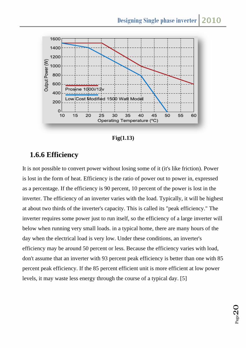
1.6.5 Effect of Operating Temperature
The power output of an inverter is dramatically decreased as its internal temperature
rises (this is sometimes called its 5, 10 & 30 minute rating; but in reality if the
inverter cannot remove the heat quick enough, then the power will rapidly drop off).
Many of our models are rated at a staggering 40°C, such as Prosine, with a classic
comparison between a Pro sine 1000 and a low cost 1500watt modified as follows.
The following chart provides a comparison between the Prosine 1000i rated at 40°C
and a common 1500watt inverter rated at 25°C. [5]
Designing Single phase inverter
Pa
ge2
0
Fig(1.13)
1.6.6 Efficiency
It is not possible to convert power without losing some of it (it's like friction). Power
is lost in the form of heat. Efficiency is the ratio of power out to power in, expressed
as a percentage. If the efficiency is 90 percent, 10 percent of the power is lost in the
inverter. The efficiency of an inverter varies with the load. Typically, it will be highest
at about two thirds of the inverter's capacity. This is called its "peak efficiency." The
inverter requires some power just to run itself, so the efficiency of a large inverter will
below when running very small loads. in a typical home, there are many hours of the
day when the electrical load is very low. Under these conditions, an inverter's
efficiency may be around 50 percent or less. Because the efficiency varies with load,
don't assume that an inverter with 93 percent peak efficiency is better than one with 85
percent peak efficiency. If the 85 percent efficient unit is more efficient at low power
levels, it may waste less energy through the course of a typical day. [5]

Designing Single phase inverter
Pa
ge2
1
CHAPTER (2)
PRACTICAL PART
2.1 DESIGN DESCRIPTION
Hardware
Software
Design

Designing Single phase inverter
Pa
ge2
2
2.2 BLOCK DIAGRAMS
OVERALL BLOCK DIAGRAM
ALGORITHMIC BLOCK DIAGRAM
Designing Single phase inverter
Pa
ge2
3
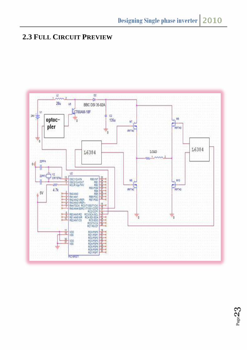
2.3 FULL CIRCUIT PREVIEW

Designing Single phase inverter
Pa
ge2
4
2.4 Hardware
DC chopper
H bridge inverter
low Pass Filter
(RLC)
Gate drive
Optocoupler

Designing Single phase inverter
Pa
ge2
5
DC CHOPPER
A dc chopper is a dc-to-dc voltage converter that we used to step up voltage from 24V
to 300v Dc.
The following circuit represents the circuit which we connected it practically.
Fig (2.1)
As we know there are two operation modes according to the inductor current, the
equations of the discontinuous mode are different from the continuous mode
equations:
Vo = Vi *(1 + (1+ (4D^2)/K) ^0.5)) / 2 ………………….. 2.1[6]
Where D is the duty ratio
D = Ton/Toff
And K = (2 * L)/ (R +Ts)
Where L: circuit’s inductor
Ts: 1 / switching frequency

Designing Single phase inverter
Pa
ge2
6
To find the circuit’s capacitance we should determine the maximum current that can
go through the load:
Iomax = Vo / R
C ≥ Iomax * (1- ((2* L) / (R * Ts)) ^0.5) / fs *ΔVo ……………………………2.2[6]
Requirements and specifications:
The required circuit must step up the voltage from 24V to 220Vrms, with ripple less
than 1%. In this section a 250 watts booster was designed.
Booster’s design and components:
Choosing L = 28uH, f = 25000, Io max = 0.85A.
Substituting in (2.2), and trying multiple simulations, the best result was when
C = 135 uF,
D = 0.75.
Figure (2.2) shows the output voltage simulation in the boost converter.

Designing Single phase inverter
Pa
ge2
7
Fig (2.2)
The IGBT chosen was CT60AM-18F which can operate under the designed booster’s
conditions. The CT60AM-18F has the datasheet shown in appendix (C).
The diode chosen was 40HFL diode, which can stand with the booster’s amperes and
voltages. The pulse generator contains a pulse signal from PIC (0V – 5V), followed by
inverter logic circuit to invert this signal (5V- 0V), followed by optocoupler in order to
have a signal (0V -15V), because the IGBT triggering at 10V (at VGE) as a minimum
voltage .C4X9 is the optocoupler .you can use a gate drive L6384 instead of the
inverter logic circuit and the optocoupler. We used inverter logic circuit followed by
the optocoupler.

Designing Single phase inverter
Pa
ge2
8
FIG (2.3) CONVERTER PRACTICAL
OPTOCOUPLER
To the IGBT transistor in the converter we need a frequency generator on an IGBT
Gate. in our project we use a PIC microcontroller to generate such needed frequency,
but the problem in PIC output signal is it’s maximum output is 5V which is very low
to drive an power IGBT that need gate voltages in range (10-20)V. So we go toward
isolator to generate like that voltage ranges, there are many types and we work on the
following type.
Opto-coupler Isolator:
The general purpose optocouplers consist of a gallium arsenide infrared emitting diode
driving a silicon phototransistor in a 4-pin dual in-
Designing Single phase inverter
Pa
ge2
9
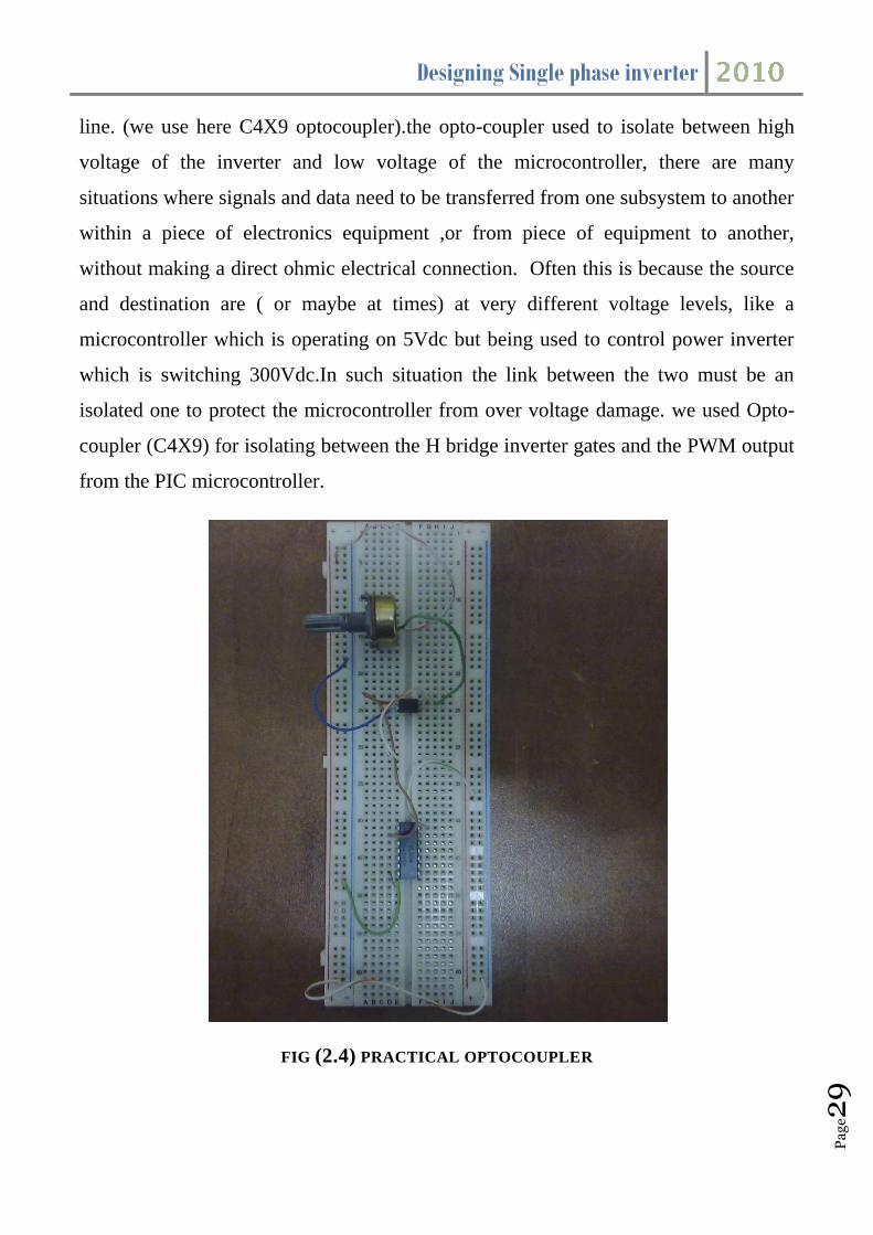
line. (we use here C4X9 optocoupler).the opto-coupler used to isolate between high
voltage of the inverter and low voltage of the microcontroller, there are many
situations where signals and data need to be transferred from one subsystem to another
within a piece of electronics equipment ,or from piece of equipment to another,
without making a direct ohmic electrical connection. Often this is because the source
and destination are ( or maybe at times) at very different voltage levels, like a
microcontroller which is operating on 5Vdc but being used to control power inverter
which is switching 300Vdc.In such situation the link between the two must be an
isolated one to protect the microcontroller from over voltage damage. we used Opto-
coupler (C4X9) for isolating between the H bridge inverter gates and the PWM output
from the PIC microcontroller.
FIG (2.4) PRACTICAL OPTOCOUPLER

Designing Single phase inverter
Pa
ge3
0
H BRIDGE INVERTER
H bridge inverter is used to convert DC voltage to AC voltage, and as we saw in
theoretical part it consist from four mosfet transistors and we use (IRF740), on the
other hand the data sheet of transistor in appendix(C). And the following fig shows the
practical H Bridge that we designed it in our project.
Fig (2.5) practical H Bridge

Designing Single phase inverter
Pa
ge3
1
Gate drive
Gate drive is required to supply the switches such as IGBTs and
MOSFETs with required voltages and currents since the PIC
couldn’t supply the required values. Gate drive L6384 was
chosen then to drive the required switches and it finally it
worked by the date of writing this report, figure (2.6) shows the
gate drive layout.
The Upper (Floating) Section is enabled to work with voltage Rail up to 600V. The
Logic Inputs are CMOS/TTL compatible for ease of interfacing with controlling
devices. Matched delays between Lower and Upper Section simplify high frequency
operation. Dead time setting can be readily accomplished by means of an external
resistor.
Fig (2.6)

Designing Single phase inverter
Pa
ge3
2
As we can see in fig (2.6) the outputs of gate drive are the input of the gate transistors
and pin 6 toward to the output (load) and that to add the voltage of the load to the
voltage in the gate of upper transistor (pin 7),on the other hand this addition because
VGS means (VG – VS ) which its the voltage that drive the transistor and this is the
reason that we use this gate drive not optocoupler; to drive the gates of transistors.
To be more understand about the work of gate drive and to ensure that it work
correctly we make an expiremant on this chip with half bridge transistor and we put
the input voltage of the system is 20V(H.V. ) . the circuit and waveforms are shown
below:
-The circuit of the experiment:
Fig 2.7

Designing Single phase inverter
Pa
ge3
3
-Gate drive input: pulses with magnitude 5 V
Fig 2.8
-Gate drive output: (on pin 6, note load voltage 20Vis the same H.V.)
Fig 2.9

Designing Single phase inverter
Pa
ge3
4
-Gate drive output: (on pin 7, note output voltage 35V which is load
voltage + gate voltage)
Fig (2.10)
-Gate drive output :( pin 5 which is 15V)
Fig 2.11

Designing Single phase inverter
Pa
ge3
5
RLC Filter
The RLC filter is used to have an approximately sinewave at the output of H Bridge.
Fig 2.12 H Bridge with LPF
Where RCL circuit represents LPF see the following.
Fig 2.13
We design this LPF depending on the following points and equations:
-A second order RLC passive filter is used at the output stage.
-The cut-off frequency should be a little higher than 50Hz.

Designing Single phase inverter
Pa
ge3
6
The cut-off frequency of a second order RLC filter is determined by the following
equations:
( )
|
|
At cut of frequency
|
|
√
To solve fc apply the equation 2.5, see the following steps
√( ) ( )
√
So, ( ) ( )
√( ) ( )
Then,

Designing Single phase inverter
Pa
ge3
7
And,
So ,to have fc near 50HZ you must choose a special values for R ,L ,C .
Then we choose these values as follows R=8Ω, L=30mH, C=150µF.
Then
2.6 Software design
Fig 2.14
After constructing the basic circuit of the PIC microcontroller 16F877,and
programmed it we use port C ( pin RC1) to output pulses for converter and also port C
( pin RC1 & RC2 ) to SPWM for H bridge.

Designing Single phase inverter
Pa
ge3
8
SPWM (sinusoidal pulse width modulation) signal generation
In this type of the modulation the control voltage (Vc) has a sinusoidal waveform.
This control voltage is compared with a triangular waveform to obtain the gates
signals of the inverter switches. the triangular waveform is maintained at constant
amplitude (Vt) and its frequency called switching or carrier frequency. While the
control voltage magnitude (Vc) could be varied to obtain different values of the
modulation index, where the modulation index (M) is the ratio of Vc to Vt.
i.e. M= Vc/Vt
The fundamental frequency of the inverter equals the control voltage frequency. The
frequency modulation index (mf) is defined as the ratio of the switching frequency (fs)
to fundamental frequency (f1).
i.e. mf = fc/f1
In this project bi-polar SPWM was used. In this type of modulation a single sinusoidal
waveform is compared with a triangular. Figure (2.13) shows a bi-polar SPWM with
modulation index of 0.7 and frequency modulation index of 10. Note that when
VC >Vt then there is a positive voltage and when VC < Vt there is no voltage. So, this
signal could be used as a gate signal for the inverter switch.
Fig 2.15

Designing Single phase inverter
Pa
ge3
9
The designed inverter has a required output voltage is of 220Vrms and a frequency of
50Hz.
The output voltage of the inverter is specified in the equation (2.9).
Vo(t) = M*VDC*sin(wt) + harmonics ………………...…………………….(2.9)[6]
Since VDC is equal to 220Vrms, then choosing M to be 1 and using equation (2.9)
results in an AC output with a magnitude of 220Vrms.
Hence, the required inverter is an inverter with a modulation index of 1, output voltage
of 220Vrms, and a fundamental frequency of 50Hz. Also to eliminate the harmonics
that above 50Hz we deigned RLC filter and it was connected after H Bridge.
Experimental results:
After programming the PICs; they were tested in order to show the output signals.
Figure (2.16) shows the booster required signal which was generated by the PIC and
displayed using the oscilloscope.
Fig 2.16
Designing Single phase inverter
Pa
ge4
0
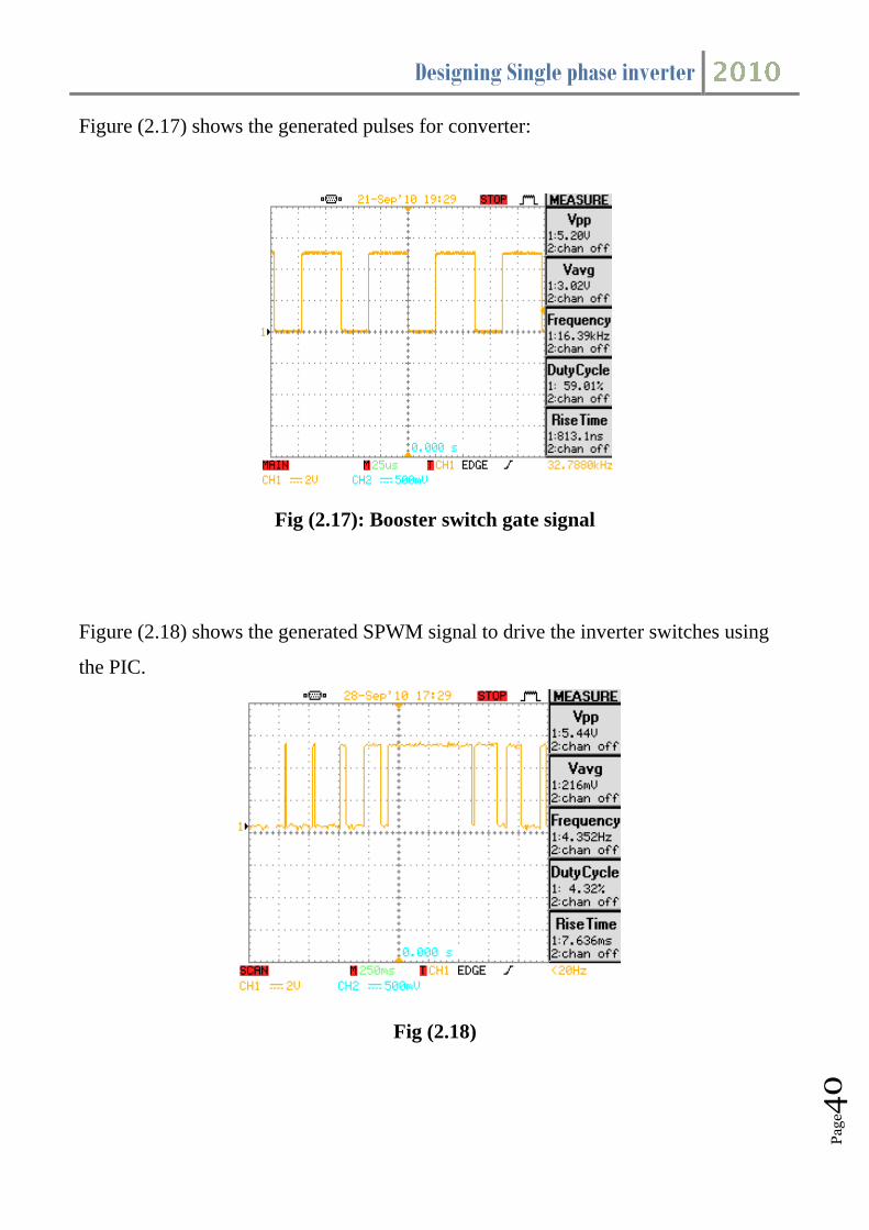
Figure (2.17) shows the generated pulses for converter:
Fig (2.17): Booster switch gate signal
Figure (2.18) shows the generated SPWM signal to drive the inverter switches using
the PIC.
Fig (2.18)

Designing Single phase inverter
Pa
ge4
1
CHAPTER (3)
PROBLEMS & CONSTRAINTS
While processing the project stages, SO many tough problems faced us. So, in
this section each problem or constraint is illustrated deeply. Also we explained
how we solved each one .

Designing Single phase inverter
Pa
ge4
2
PROBLEM #1
DC-CHOPPER:
After we finished connecting the booster circuit, we didn't find a dc supply having
30A as a maximum current because the peak current goes through the inductor reaches
30A according to the following analysis on MATLAP PROGRAM (shown in
appendix (B) for the booster circuit, so we didn't test this circuit practically.
SOLUTION: Because we can't apply the booster converter practically, we thought about any
alternatives that instead of using booster converter. So we using transformer.
How can you use the transformer?
- Now you have 24Vm (17Vrms) at the drain of the above mosfets in H Bridge,
because the booster converter didn’t work practically .here you must use a special type
of transformer at the output of H Bridge which is called a pulse transformer (step up
voltage 17/220Vrms) . the following point increases your information about pulse
transformer.
- A pulse transformer for use in a system which transmits digital signals in the form of
pulses, e.g., an ISDN, is a wide-band transformer which is mainly intended for the
waveform transmission. Pulse transformers are designed to maintain the input pulse
waveform and power while transforming the source impedance to a value
approximating the load impedance. In the field of electronic circuits, pulse electric
technology such as digitization of electronic computers, pulse communication and
measuring devices has been developed, and accordingly, there has been an increasing

Designing Single phase inverter
Pa
ge4
3
demand for circuit elements which exhibit a high performance in the wave-form
transmission. Electrical pulse power systems are utilized in applications including
infrared and radar pulse generating systems, microwave applications, and radiant
energy systems, including arc lamps and lasers. A common and important application
of pulse transformers is the coupling of a load resistance to a source of pulsed power.
Radar transmitters, for instance, usually employ an output power tube such as a
magnetron, which must be driven at a relatively high voltage and high impedance
level. Like conventional transformers, pulse transformers typically consist of an input
winding, an output winding, and a core structure of ferromagnetic material to transfer
energy from the input winding to the corresponding output winding. Magnetic
material is introduced in a special way into the central, concentric aperture of the
primary and secondary windings, so that a completely transformative transducer is
obtained. An electrical current flowing in the input winding creates a magnetomotive
force which induces a flux flow in the ferromagnetic material. This change in flux in
the magnetic circuit induces a current in the output winding and thereby effects the
energy transfer.[7]
- At the secondary side of the pulse transformer you can put a LPF as shown in fig
2.13 we didn't use this way because we didn't find a pulse transformer in the shops and
we didn't know how to built it .
- Now, if you put a LPF as shown in fig 2.12 → now you can use a conventional
transformer (17/220V), at the secondary side put your load.

Designing Single phase inverter
Pa
ge4
4
PROBLEM #2
GATE DRIVE
The problem in this chip not in its work but in if it is exist or not .the problem that we
face it that we need two gate drive in our project but we find one chip in the market
and the other we did not find it in our market so we are still wait, to now to get it from
other country.
PROBLEM #3
PIC MICROCONTROLLER
That when we give the PIC microcontroller a command to take an output of driving
square wave, we surprised with the result which is not in the same command, it give a
percentage of error which increase with increasing the input frequency (i.e. when
order the PIC microcontroller to give an output square wave with f=25 KHz, it give
about 16 KHz).
SOLUTION:
To solve this problem there are functions appear to you when you programming the
pic and one of these function is a packet data for pulses (PWM) and in this packet you
can put the frequency that you need not generation the frequency as we did.

Designing Single phase inverter
Pa
ge4
5
CHAPTER (4)
THE COST
Device number Price for each one
Inductor(28mH) 1 75 NIC
Capacitor (333µf) 2 30 NIC
CT60AM IGBT 1 65 NIC
40HFL diode 1 40 NIC
Optocoupler 1 10 NIC
Variable resister 3 3 NIC
PIC 2 40 NIC
Gate drive 1 45 NIC
White board 2 15 NIC
All small capacitors 10 NIC
All small resistors 10 NIC
Irf540 mosfets 4 15 NIC
Total cost = 500 NIC

Designing Single phase inverter
Pa
ge4
6
CHAPTER (5)
CONCLUSION AND RECOMMENDATION
Everyone knows that the university must do more technological projects, so the
university managers and many teachers and students attend to do these projects.
Our teacher told us to do a good inverter project, we accepted this and started
working last year.
We know by experiment that applying practical complex project is more
different than learning theoretical courses.
Applying any practical project needs more things such as studying with more
concentration and thinking about your project.
In other hand, many practical problems face you when you applying your
project such as the lack of your components project in the market, and the
components operating problems.
Don’t forget the problem of high prices for some components.
As advice, applying our project needs carefully using for all components.
especially using the gate drive, and PIC.
We hope that the university managers help the students in buying many suitable
components that the students need it, and buying modern measuring devices.

Designing Single phase inverter
Pa
ge4
7
CHAPTER (6)
Appendix

Designing Single phase inverter
Pa
ge4
8
Appendix A
In this appendix we show the two PIC codes which we use them.
The PIC code that uses to have two SPWM signals as follows
#include <16f877a.h> //tells the compiler that we use PIC16F877A.
#device ADC=10 // using 16bit ADC converter.
#include<math.h> // library (math.h) is added
#fuses HS,NOWDT,NOPROTECT
#use delay(clock=20000000) // high speed clock 20MHz.
signed int triangular[20]= -10,-8,-6,-4,-2,0,2,4,6,8,10,8,6,4,2,0,-2,-4,-6,-8; // defined
values for the triangular signals
double s,tr;
int h=0;
int n=0;
void main()
set_tris_a(0x0F);
set_tris_b(0x0F);
set_tris_c(0x00);
set_tris_d(0x00);
while(1)
output_high(PIN_C3);
s=10.0*sin((double)pi*h/90.0); // defining sinusoidal signal with a magnitude of 10, so
the modulation index will be equal to 1. To get modulation index of 0.7, this signal
magnitude must be 7.0.
tr= triangular[n];

Designing Single phase inverter
Pa
ge4
9
if(s>tr) // comparing the sinusoidal signal with the triangular one
output_high(PIN_C1);
output_low(PIN_C2); // used for generating complement signal
else
output_low(PIN_C1);
output_high(PIN_C2);
delay_us(111);
if(n==19)
n=1;
if(h==179)
h=0;
n++;
h++;
The PIC code that uses as an input signal for the IGBT in the booster converter
#include <16f877a.h> //tells the compiler that we use PIC16F877A.
#device ADC=10 // using 16bit ADC converter.
#fuses HS,NOWDT,NOPROTECT
#use delay(clock=20000000) // high speed clock 20MHz (oscillator).
void main()
set_tris_a(0x0F); // Set 4 pins of port A as inputs
set_tris_b(0x00); // Set port B as output

Designing Single phase inverter
Pa
ge5
0
set_tris_c(0x00); // Set port C as output
set_tris_d(0x00); // Set port D as output
while(1) // Use infinite loop
output_high(PIN_C3); // Pin C3 is on (used to insure that the PIC is operating)
output_high(PIN_C1); // Turn on Pin C3
delay_us(30); // Pin C1 is on for 30us.
output_low(PIN_C1); // Turn off pin C1
delay_us(10); // Pin C1 is off for 10us

Designing Single phase inverter
Pa
ge5
1
Appendix B
This appendix shows the matlab analyses for our practical circuits
1-booster converter output

Designing Single phase inverter
Pa
ge5
2
Fig (6.1)
2-H Bridge output without LPF:

Designing Single phase inverter
Pa
ge5
3
Fig 6.2

Designing Single phase inverter
Pa
ge5
4
3- H Bridge with RLC FILTER

Designing Single phase inverter
Pa
ge5
5
Fig 6.3

Designing Single phase inverter
Pa
ge5
6
Appendix c
This appendix talks about the datasheets for all components in this project .
*CT60AM 18F IGBT :
- General datasheet
Fig 6.4 data sheet for CT60AM 18F
- Genaral characteristics
• VCES ............................................................................... 900V
• IC .........................................................................................60A
• Integrated Fast-recovery diode
• Small tail loss
• Low VCE(sat)
- APPLICATION
Microwave oven, Electromagnetic cooking devices, Rice-cookers.
- Main characteristic table

Designing Single phase inverter
Pa
ge5
7
Symbol Parameter Conditions Ratings Unit
VCES Collector-Emitter
Voltage
VGE = 0V 900 V
VGES Gate-Emitter Voltage ±25 V
VGEM Peak Gate-Emitter
Voltage
±30 V
IC Collector Current 60 A
ICM Collector Current
(Pulse
120 A
IE Emitter Current 40 A
PC Maximum Power
Dissipation
180 W
Tj Junction Temperature –40 ~ +150 °C
Tstg Storage Temperature –40 ~ +150 °C
Fig 6.5 main characteristic table for CT60AM 18F
- Operating curves

Designing Single phase inverter
Pa
ge5
8
Fig 6.6 operating curves for CT60AM 18F
PC8171xNSZ0F Series OPTOCOUPLER:
- DISCRIPTION
PC8171xNSZ0F Series contains an IRED optically
coupled to a phototransistor.
It is packaged in a 4pin DIP, available in SMT gullwing
lead-form option.
Input-output isolation voltage(rms) is 5.0kV.
Collector-emitter voltage is 80V, CTR is 100% to
600% at input current of 0.5mA and CMR is MIN.
- APPLICATION

Designing Single phase inverter
Pa
ge5
9
1. Programmable controllers
2. Facsimiles
3. Telephones
- FEATURES
1. 4pin DIP package
2. Double transfer mold package (Ideal for Flow Soldering)
3. Low input current type (IF=0.5mA)
4. High collector-emitter voltage(VCEO : 80V)
5. High noise immunity due to high common rejection
voltage (CMR : MIN. 10kV/μs)
6. High isolation voltage between input and output
(Viso(rms) : 5.0 kV)
7. Lead-free and RoHS directive compliant
- INTERNAL CONNECTION DAIGRAM
Fig 6.7 internal connection diagram for optocoupler
- ABSOLUTE MAXIMUM RATING

Designing Single phase inverter
Pa
ge6
0
Fig 6.8 maximum values table for optocoubler
- ELECTRO – OPTICAL CHARACTEREISTIC
Fig 6.9 electro-optical characteristics table for optocoubler
- GENERAL CONNECTION CIRCUIT

Designing Single phase inverter
Pa
ge6
1
Fig 6.10 general connection circuit for optocoubler
* L6384 GATE DRIVE :
- DISCRIPTION
The L6384 is an high-voltage device. It has an Half - Bridge Driver structure that
enables to drive N Channel Power MOS or IGBT. The Upper (Floating) Section is
enabled to work with voltage Rail up to 600V. The Logic Inputs are CMOS/TTL
compatible for ease of interfacing with controlling devices. Matched delays between
Lower and Upper Section simplify high frequency operation. Dead time setting can be
readily accomplished by means of an external resistor.
- General characteristics
HIGH VOLTAGE RAIL UP TO 600 V
dV/dt IMMUNITY +- 50 V/nsec IN FULL TEMPERATURE RANGE
DRIVER CURRENT CAPABILITY:
400 mA SOURCE,
650 mA SINK
SWITCHING TIMES 50/30 nsec RISE/FALL WITH 1nF LOAD
CMOS/TTL SCHMITT TRIGGER INPUTS WITH HYSTERESIS AND PULL
DOWN
SHUT DOWN INPUT
DEAD TIME SETTING
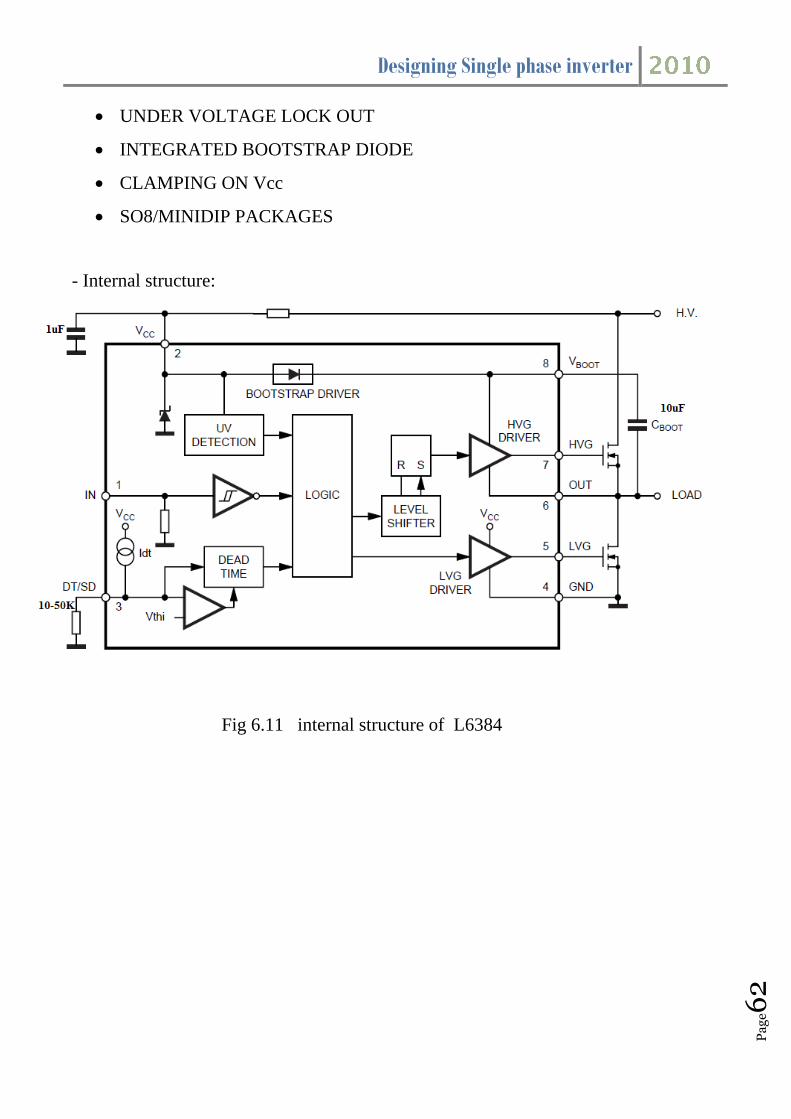
Designing Single phase inverter
Pa
ge6
2
UNDER VOLTAGE LOCK OUT
INTEGRATED BOOTSTRAP DIODE
CLAMPING ON Vcc
SO8/MINIDIP PACKAGES
- Internal structure:
Fig 6.11 internal structure of L6384

Designing Single phase inverter
Pa
ge6
3
- Main characteristic table
N. name Type Function
1 IN(*) 1 Logic Input: it is in phase with HVG and in opposition
of phase with LVG. It is
compatible to Vcc voltage
2 VCC 1 Supply input voltage: there is an internal clamp [Typ.
15.6V]
There is also an UVLO feature ( Typ. Vccth1 = 12V,
Vccth2 = 10V).
3 DT/SD 1 High impedence pin with two functionalities. When
pulled to a voltage lower than Vdt
[Typ.0.5V] the device is shut down. A voltage higher
than Vdt sets the dead time
between high side and low side gate driver. The dead
time value can be set forcing a
certain voltage level on the pin or connecting a resistor
between pin 3 and ground.
Care must be taken to avoid spikes on pin 3 that can
cause undesired shut down of
the IC. For this reason the connection of the components
between pin 3 and ground
has to be as short as possible. This pin can not be let
floating for the same reason.
The pin has not to be pulled through a low impedence to
Vcc, because of the drop on
the corrent source that feeds Rdt. The operative range is:
Vdt ... 270K V Idt, that allows
a dt range of 0.4 - 3.1ms

Designing Single phase inverter
Pa
ge6
4
4 GND Ground
5 LVG 0 Low side driver output: the output stage can deliver
400mA source and 650mA sink
[Typ. Values].
The circuit guarantees 0.3V max on the pin (@Isink =
10mA) with Vcc > 3V and lower
than the turn on threshold. This allows to omit the
bleeder resistor connected between
the gate and the the source of the external mosfet
normally used to hold the pin low;
the gate driver ensures low impedence also in SD
conditions.
6 Vout 0 Upper driver floating reference: layout care has to be
taken to avoid undervoltage
spikes on this pin
7 HVG 0 High side driver output:the output stage can deliver
400mA source and 650mA sink
[Typ. Values].
The circuit guarantees 0.3V max between this pin and
Vout (@Isink = 10mA) with Vcc >
3V and lower than the turn on threshold. This allows to
omit the bleeder resistor
connected between the gate and the the source of the
external mosfet normally used
to hold the pin low; the gate driver ensures low
impedence also in SD conditions.
8 Vboot Bootstrap Supply Voltage: it is the upper driver floating
supply. The bootstrap
capacitor connected between this pin and pin 6 can be

Designing Single phase inverter
Pa
ge6
5
fed by an internal structure
named ”bootstrap driver” (a patented structure). This
structure can replace the
external bootstrap diode.
Fig 6.12 main characteristic table for L6384
*IRF740 MOSFET N-CHANNEL
- General datasheet
Fig 6.13 datasheet for IRF740
- General informations
• TYPICAL RDS(on) = 0.46Ω
• EXCEPTIONAL dv/dt CAPABILITY
• 100% AVALANCHE TESTED
• LOW GATE CHARGE
• VERY LOW INTRINSIC CAPACITANCES

Designing Single phase inverter
Pa
ge6
6
- DESCRIPTION
The PowerMESH™II is the evolution of the first generation
of MESH OVERLAY™. The layout refinements
introduced greatly improve the Ron*area
figure of merit while keeping the device at the leading
edge for what concerns swithing speed, gate
charge and ruggedness.
- APPLICATIONS
• HIGH-EFFICIENCY DC-DC CONVERTERS
• UPS AND MOTOR CONTROL
- General characteristic table
Symbol Parameter Value unit
VDS Drain-source Voltage (VGS = 0) 400 V
VDGR Drain-gate Voltage (RGS = 20 kΩ 400 V
VGS Gate- source Voltage ± 20 V
ID Drain Current (continuos) at TC =
25°C
10 A
ID Drain Current (continuos) at TC =
100°C
6.3 A
IDM (l) Drain Current (pulsed) 40 A
PTOT Total Dissipation at TC = 25°C 125 A
Derating Factor 1.0 W/°C
dv/dt(1) Peak Diode Recovery voltage slope 4.0 V/ns
Tstg Storage Temperature – 65 to 150 °C
Tj Max. Operating Junction Temperature – 65 to 150 °C
Fig 6.14 general characteristic table for IRF740
- Operating curves

Designing Single phase inverter
Pa
ge6
7
Fig 6.15 operating curves for IRF740

Designing Single phase inverter
Pa
ge6
8

Designing Single phase inverter
Pa
ge6
9

Designing Single phase inverter
Pa
ge7
0

Designing Single phase inverter
Pa
ge7
1
(1.5)


![مشروع RF[1]](https://static.fdocuments.in/doc/165x107/55cf92af550346f57b98b24f/-rf1.jpg)
![مشروع نظام الاتصالات - citc.gov.sa A... · d-úä.]g i Communications and Information Technology Commission . d-úä.]g i Communications and Information Technology](https://static.fdocuments.in/doc/165x107/5dd0be73d6be591ccb627b89/-citcgovsa-a-d-g-i-communications.jpg)


