© 2014 Gyungseon Seol - ufdcimages.uflib.ufl.edu
146
DEVICE SIMULATION OF FUNCTIONALIZED 2D MATERIAL By GYUNGSEON SEOL A DISSERTATION PRESENTED TO THE GRADUATE SCHOOL OF THE UNIVERSITY OF FLORIDA IN PARTIAL FULFILLMENT OF THE REQUIREMENTS FOR THE DEGREE OF DOCTOR OF PHILOSOPHY UNIVERSITY OF FLORIDA 2014
Transcript of © 2014 Gyungseon Seol - ufdcimages.uflib.ufl.edu

DEVICE SIMULATION OF FUNCTIONALIZED 2D MATERIAL
By
GYUNGSEON SEOL
A DISSERTATION PRESENTED TO THE GRADUATE SCHOOL OF THE UNIVERSITY OF FLORIDA IN PARTIAL FULFILLMENT
OF THE REQUIREMENTS FOR THE DEGREE OF DOCTOR OF PHILOSOPHY
UNIVERSITY OF FLORIDA
2014

© 2014 Gyungseon Seol

To my family

4
ACKNOWLEDGMENTS
I would like to express my deepest gratitude to my advisor, Prof. Jing Guo, for
his excellent guidance, caring and patience. Studying as a student of Prof. Guo
has been a great privilege that not much Ph.D. student would be lucky enough to
have.
It is a great pleasure to thank my colleagues. I thank Dr. Kai Tak Lam and Dr.
Yang Lu, for all the discussions. It had been great joy to work with Dr. Wenchao
Chen, Dr. Qun Gao, Leitao Liu, Xi Cao, Zhipeng Dong and Runlai Wan.
Finally I want to thank my wife and my daughter.
This work was supported by ONR, ARL, and NSF.

5
TABLE OF CONTENTS page
ACKNOWLEDGMENTS .................................................................................................. 4
LIST OF TABLES ............................................................................................................ 8
LIST OF FIGURES .......................................................................................................... 9
LIST OF ABBREVIATIONS ........................................................................................... 11
ABSTRACT ................................................................................................................... 12
CHAPTER
1 INTRODUCTION .................................................................................................... 14
1.1. Overview .......................................................................................................... 14
1.2. Graphene Based Electronics ........................................................................... 15 1.2.1. Tight Binding Approach of Graphene Electronic Properties ................... 16 1.2.2. Electronic Properties of Armchair Graphene Nanoribbon ....................... 17
1.3. Outline ............................................................................................................. 18
2 BANDGAP OPENING IN BORON NITRIDE CONFINED ARMCHAIR GRAPHENE NANORIBBON ................................................................................... 22
2.1. Overview .......................................................................................................... 22
2.2. Simulation Method ........................................................................................... 23 2.3. Results ............................................................................................................. 24 2.4. Summary ......................................................................................................... 28
3 PERFORMANCE PROJECTION OF GRAPHENE NANOMESH AND NANOROAD TRANSISTORS ................................................................................. 33
3.1. Overview .......................................................................................................... 33 3.2. Approach ......................................................................................................... 35 3.3. Results ............................................................................................................. 36
3.3.1. DFT Results : E-k Dispersion Relation ................................................... 36 3.3.2. DFT Results : Binding Energy Calculation Using Basis Set
Superposition Error (BSSE) .......................................................................... 38 3.3.3. Device Performance ............................................................................... 39
3.4. Summary ......................................................................................................... 41
4 n-DOPING OF TRANSITION METAL DICHALCOGENIDES BY POTASSIUM ...... 48
4.1. Overview .......................................................................................................... 48 4.2. Method ............................................................................................................. 49

6
4.3. Results ............................................................................................................. 51
4.4. Summary ......................................................................................................... 52
5 STRAIN INDUCED INDIRECT TO DIRECT BANDGAP TRANSITION IN BI-LAYER WSE2 ......................................................................................................... 57
5.1. Overview .......................................................................................................... 57 5.2. Method ............................................................................................................. 59 5.3. Results ............................................................................................................. 61 5.4. Summary ......................................................................................................... 65
6 ELECTROSTATIC SCREENING PROPERTIES OF MULTILAYER MOS2 ............ 75
6.1. Overview .......................................................................................................... 75
6.2. Method ............................................................................................................. 76 6.3. Results ............................................................................................................. 78 6.4. Summary ......................................................................................................... 83
7 TWO DIMENSIONAL HETEROJUNCTION DIODE AND TRANSISTOR ............... 88
7.1. Overview .......................................................................................................... 88 7.1. Graphene-MoS2 Junction Diode ...................................................................... 90
7.1.1. One Dimensional Simulation for Vertical Junction .................................. 90 7.1.2. Classical Transport Calculation .............................................................. 92 7.1.2. Two Dimensional Simulation to Treat Lateral Variations ........................ 93
7.2. MoS2-Graphene-MoS2 Bipolar Junction Transistor .......................................... 95 7.2.1. 1D Capacitance Model with NEGF Transport Calculation ...................... 95
7.2.2. Results of the MGM BJT ........................................................................ 97 Summary .............................................................................................................. 100
8 CONCLUSION ...................................................................................................... 108
APPENDIX
A BANDGAP CALCULATION OF AGNR AND AGNR WITH EDGE PERTURBED BY THE IONIC POTENTIAL ................................................................................. 111
B BASIS SET SUPERPOSITION ERROR ............................................................... 119
C G0W0 CALCULATION APPROACH ...................................................................... 122
D VASP INPUT SCRIPT FOR GGA, HSE AND G0W0 SIMULATION ...................... 123
E ANALYTICAL DERIVATION OF DEBYE LENGTH .............................................. 127
F EVALUATION OF 2D THOMAS-FERMI MODEL ................................................. 130
G INTERLAYER COUPLING FACTOR αC AND αN .................................................. 132

7
H EXTRACTION OF INTERLAYER COUPLING FACTOR AND RELATION TO NEGF .................................................................................................................... 134
LIST OF REFERENCES ............................................................................................. 137
BIOGRAPHICAL SKETCH .......................................................................................... 146

8
LIST OF TABLES
Table page 2-1 Tight binding parameters for A-Cx(BN)ys ............................................................ 29
3-1 Summary of the MOSFET performance ............................................................. 42
4-1 Summary of bonding properties of MoS2 and graphene ..................................... 53
5-1 DFT calculated structural parameters ................................................................. 67
5-2 DFT calculated BL WSe2 bandgap ..................................................................... 68
7-1 Scattering potential matrix element value ......................................................... 101
D-1 GGA step 1 and 2 ............................................................................................. 123
D-2 GGA step 3 ....................................................................................................... 124
D-3 GGA step 4 ....................................................................................................... 124
D-4 HSE Self-consistent calculation ........................................................................ 125
D-5 HSE Band calculation ....................................................................................... 125
D-6 HSE Band calculation INCAR file. .................................................................... 126
G-1 Classical and NEGF transport calculation comparison ..................................... 133

9
LIST OF FIGURES
Figure page 1-1 Schematic of 2D graphene and corresponding lattic vectors.. ............................ 20
1-2 Schematic of an AGNR and a ZGNR. ................................................................ 21
2-1 Schematic of an A-Cx(BN)ys. calculation. ........................................................... 29
2-2 Bandgap properties and C to C distance as a function of AGNR and A-Cx(BN)ys width. ................................................................................................... 30
2-3 A Pseudocharge density plot of A-Cx(BN)y and H-terminated AGNR. ................ 31
2-4 DFT and TB model bandgap calculation comparison. ........................................ 32
3-1 Schematic of the device structure and the top-of-barrier ballistic transistor model. ................................................................................................................. 43
3-2 Schematic of the graphene Nanoroad and the bandgap properties.. ................. 44
3-3 Schematic of the graphene nanomesh and the bandgap properties. ................. 45
3-4 C-H and C-F binding energy of A-XNR structures with Na=3 or 4. ..................... 46
3-5 The ballistic performance limits of Graphene nanoroad FETs compare to Si.. ... 46
3-6 The ballistic performance limits of Graphene nanomesh FETs compare to Si and GaAs. .......................................................................................................... 47
3-7 A-HNRs and A-FNRs device performance comparison. ..................................... 47
4-1 DFT calculated structures of K doped graphene and MoS2. ............................... 54
4-2 K to graphene, MoS2 and WSe2 binding energy comparison. ............................ 55
4-3 Charge density plot of K-doped graphene and K-doped MoS2. .......................... 55
4-4 Charge transfer calculated using Bader analysis ................................................ 56
5-1 Schematic of bi-layer WSe2 and the mechanical strain setup. ............................ 69
5-2 DFT calculated E-k relations of bi-layer WSe2, comparing the XC functions and the effect of including and excluding spin-orbital coupling (SOC). ............... 70
5-3 Comparison of the bandgap features of BL-WSe2. ............................................. 71
5-4 Comparison of PL measurement with HSE-DFT calculation. ............................. 72

10
5-5 Bandgap features of ML WSe2. .......................................................................... 73
5-6 ML WSe2 atomic and orbital contribution on the E-k relation. ............................. 74
5-7 The partial charge calculation of at each band points of interest. A) KC, B) Σ and C) ΓV. The energy range specified in sub-figure represents the integration interval. ............................................................................................. 74
6-1 Schematic of multi-layer MoS2, and 1D capacitance model. .............................. 84
6-2 Normalized charge density profile in 10 layer of MoS2 FET with varying gate charge density. ................................................................................................... 85
6-3 Effective screening length in 10 layers of MoS2 FET with varying gate charge density.. .............................................................................................................. 85
6-4 Effective screening length between the first (bottom) two layers( i=1, λeff) compared with the Debye length (λD
i) at different temperatures. ........................ 86
6-5 Charge and potential profile along the MoS2 stack. ............................................ 87
7-1 Simulated structure of graphene-MoS2 junction. .............................................. 101
7-2 MoS2-Graphene junction properties. ................................................................ 102
7-3 Band alignment results of 2D Poisson calculation. ........................................... 103
7-4 Isolated diode model and its results. ................................................................ 104
7-5 Schematic of the 3 terminal MGM BJT and NEGF current calculation results. . 105
7-6 Current gain and intrinsic delay of the MGM-BJT.. ........................................... 106
A-1 Graphene nanoribbon schematic. ..................................................................... 111
A-2 Schematic of AGNR and perturbation modeling. .............................................. 115
B-1 BSSE calculation method. ................................................................................ 121
C-1 Bilayer WSe2 HSE-DFT and G0W0 calculation. ................................................ 122

11
LIST OF ABBREVIATIONS
1D 1 dimensional
2D 2 dimensional
3D 3 dimensional
ABNNR Armchair boron nitride nanoribbon
AGNR Armchair graphene nanoribbon
BNNR Boron nitride nanoribbon
BSSE Basis set superposition error
CMOS Complimentary metal-oxide-semiconductor
CP Counter poise
CVD Chemical vapor deposition
DFT Density-functional theory
DIBL Drain induced barrier lowering
DIBT Drain induced barrier thinning
DOS Density of states
FET Field effect transistor
GNR Graphene nanoribbon
h-BN hexagonal boron nitride
ITRS International technology roadmap for semiconductors
I-V Current-voltage
MOSFET Metal semiconductor field effect transistor
NEGF Non-equilibrium Green's function
TB Tight binding
TMD Transition metal dichalcogenides

12
Abstract of Dissertation Presented to the Graduate School of the University of Florida in Partial Fulfillment of the Requirements for the Degree of Doctor of Philosophy
DEVICE SIMULATION OF FUNCTIONALIZED 2D MATERIAL
By
Gyungseon Seol
August 2014
Chair: Jing Guo Major: Electrical and Computer Engineering
In the recent years, since the first advent of graphene in 2004, two dimensional
(2D) semiconducting materials, such as h-BN and transition metal dichalcogenides
(TMDs) have gained of a great interest. To minimize the short channel effect at extreme
scaling of future sub-5 nm gate length field-effect transistors (FETs), large bandgap
semiconductors with ultrathin body are essential. In this context adopting 2D
semiconductors as channel will serve a great advantage. Graphene, due to its excellent
charge transport properties, ranks itself as one of the most promising future device
material. TMDs are also of great interest due to sufficient bandgap they provide, which
is desired in achieving large on-off current ratio. Combinations of these materials are
possible, leading to various device structures to be studied.
This dissertation can be categorized into to topic. The first is the Ab-initio
calculations to study the material properties of the 2D semiconductor. We present
graphene derivatives which bandgap can be engineered without reducing its
dimensionality, which is preferred in achieving higher current density when applied as
channel material of FETs. Doping properties of TMDs (MoS2 and WSe2) and effect of
strain on bilayer WSe2 are investigated. These studies served as a fundamental in

13
understanding the device operation mechanism and performance prediction, which is
the second topic of this work. Performance limit of FETs using grapehene derivative
materials is examined and show that they out-perform Si based FETs. Next, the
electrostatic screening properties of MoS2 is presented, which we predict the screening
length can be as short as half the interlayer distance of the 2D crystalline to infinite
screening length depending on the temperature and applied gate voltage. Following is
the electrical properties of Graphene-MoS2 heterojunction. To assess the mechanism of
the junction we perfrom 1D and 2D Possion calculation followed by transport calculation
using classical method and non-equilibrium green’s function formalism. Last, 3 terminal
bipolar junction transistor using MoS2- Graphene-MoS2 heterostructure is studied.

14
CHAPTER 1 INTRODUCTION
1.1. Overview
In the past few decades, scaling down the device feature size has been the
major driving force behind sustaining the growth of semiconductor industry. So far by
increasing the device density, it has successfully fulfilled its task in delivering more
functionality. However, we are now in the era of 22nm node, and the International
Technology Roadmap for Semiconductors (ITRS) 2011 suggests that in 2022, the gate
length of a metal-oxide-field-effect-transistor (MOSFET) will reach sub 10nm regime [1].
Further reduction of feature size lies as a question mark in terms of physical realization
and enhancement in the device performance. With the channel length in such extreme
scale, the gate loses its controllability, due to the drain-induced electrostatic effect that
lowers the barrier (DIBL) [2]. At the same time the barrier itself gets thinner, drain-
induced-barrier-thinning (DIBT), which results in increase of source to drain (S/D)
tunneling [3]. Both of these effects make it difficult to turn the device off, which lead to
poor power efficiency that is undesired in mobile applications. To overcome the
limitations, various new classes of materials as well as device structures have been
explored [4-6]. One approach is to make the channel thin. As the gate size shrinks, to
maintain the electrostatic control, the channel needs to be scaled down accordingly. So,
the question is, what if the channel is atomic thin.
Since the first demonstration of graphene [7], 2D layered materials have been
investigated in depth. Although graphene exhibits superior carrier mobility, the material
innately suffers from zero bandgap. Thus, employing a pristine graphene as a channel
material in the field-effect-transistor (FET), result in a low ION/IOFF ratio. This imposes a

15
major obstacle for using graphene in future digital electronic device applications. To
address this problem, few ways have been proposed to induce bandgap in a graphene
system, such as, graphene nanoribbons (GNRs), graphene nanomesh and graphene
antidot [8~11]. Also there exists other layered-structure material family with bandgap,
such as, hexagonal boron nitride (h-BN), transition metal dichalcogenides (TMDCs)
[12,13]. In this work, we theoretically investigate the material properties of such 2D
functionalized materials that can provide, or bear a sufficient bandgap and elucidate the
physics behind. Also we conduct device simulations that employ the materials as
channel to project the performance limit and compare to that of the Si MOSFET.
1.2. Graphene Based Electronics
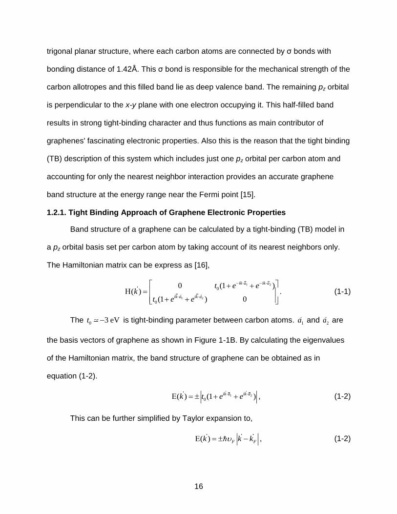
Graphene is a monolayer (ML) of carbon tightly packed into a dense 2D
honeycomb lattice as visualized in Figure 1-1A. Previously, it was studied as a building
block of carbon allotropes such as, graphite and carbon nanotubes (CNTs). It was
believed until recently, that the 2D material is unstable and cannot exist in free-state.
However, in 2004, Novoselov et al. proved this belief to be false, demonstrating by
micromechanical cleavage technique [7]. Further investigation was carried out and in
2007, the subtle optical effect created on top of a chosen SiO2 substrate allowed its
observation even with an ordinary optical microscope [14].
Carbon is the sixth element in the periodic table and is smallest atom in column
IV. A carbon atom has six electrons in 1s2, 2s2 and 2p2 orbital. Two electrons are in the
1s2 orbital and are strongly bound as core electrons. When the carbons form a
crystalline, the 4 valence electron occupying 2s2 and 2p2 orbitals give rise to 2s, 2px, 2py
and 2pz orbital. Since 2s and 2p orbital are close in energy, these orbital mix and form
sp1, sp2 and sp3 hybridization. In the case of graphene, sp2 hybridization, and forms a
16
trigonal planar structure, where each carbon atoms are connected by σ bonds with
bonding distance of 1.42Å. This σ bond is responsible for the mechanical strength of the
carbon allotropes and this filled band lie as deep valence band. The remaining pz orbital
is perpendicular to the x-y plane with one electron occupying it. This half-filled band
results in strong tight-binding character and thus functions as main contributor of
graphenes' fascinating electronic properties. Also this is the reason that the tight binding
(TB) description of this system which includes just one pz orbital per carbon atom and
accounting for only the nearest neighbor interaction provides an accurate graphene
band structure at the energy range near the Fermi point [15].
1.2.1. Tight Binding Approach of Graphene Electronic Properties
Band structure of a graphene can be calculated by a tight-binding (TB) model in
a pz orbital basis set per carbon atom by taking account of its nearest neighbors only.
The Hamiltonian matrix can be express as [16],
1 2
1 2
0
0
0 (1 )( )
(1 ) 0
ik a ik a
ik a ik a
t e ek
t e e
. (1-1)
The 0 3 eVt is tight-binding parameter between carbon atoms. 1a and 2a are
the basis vectors of graphene as shown in Figure 1-1B. By calculating the eigenvalues
of the Hamiltonian matrix, the band structure of graphene can be obtained as in
equation (1-2).
1 2
0( ) (1 )ik a ik ak t e e , (1-2)
This can be further simplified by Taylor expansion to,
( ) F Fk k k , (1-2)
17
where / 300F c is the Fermi velocity. The highly linear dispersion relation differs from
conventional semiconductors, where the energy spectrum can be approximated in
parabolic manner. Although the graphene exhibits superior carrier velocity and near
ballistic transport characteristics, it is innately a zero-bandgap. This is an unappealing
feature for nano-electronic applications.
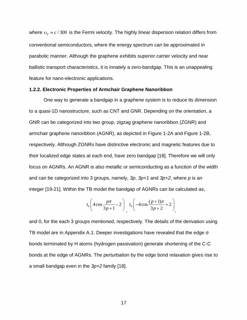
1.2.2. Electronic Properties of Armchair Graphene Nanoribbon
One way to generate a bandgap in a graphene system is to reduce its dimension
to a quasi-1D nanostructure, such as CNT and GNR. Depending on the orientation, a
GNR can be categorized into two group, zigzag graphene nanoribbon (ZGNR) and
armchair graphene nanoribbon (AGNR), as depicted in Figure 1-2A and Figure 1-2B,
respectively. Although ZGNRs have distinctive electronic and magnetic features due to
their localized edge states at each end, have zero bandgap [18]. Therefore we will only
focus on AGNRs. An AGNR is also metallic or semiconducting as a function of the width
and can be categorized into 3 groups, namely, 3p, 3p+1 and 3p+2, where p is an
integer [19-21]. Within the TB model the bandgap of AGNRs can be calculated as,
0 4cos 23 1
pt
p
, 0
( 1)4cos 2
3 2
pt
p
,
and 0, for the each 3 groups mentioned, respectively. The details of the derivation using
TB model are in Appendix A.1. Deeper investigations have revealed that the edge σ
bonds terminated by H atoms (hydrogen passivation) generate shortening of the C-C
bonds at the edge of AGNRs. The perturbation by the edge bond relaxation gives rise to
a small bandgap even in the 3p+2 family [18].

18
1.3. Outline
This work is organized as the following. Chapter 2 talks about 2D continuous
sheet of hybrid material, h-BN and Graphene. Creating domains of h-BN in graphene
has been reported. By precise control of the shape of the domain, one can engineer the
electronic properties of the graphene/h-BN hybrid material. We have conducted study
on GNRs in between BN nanoribbons (BNNRs). In this structure, the confinement of the
wave functions can be given to the AGNRs without rapid σ bond termination, thus
generate bandgap in a continuous 2D structure.
Similar approach has been studied in Chapter 3. Instead of the h-BN,
functionalized graphene was used to generate the confinement. By hydrogenation of
fluoridation, the sp2 hybridization of the graphene changes to sp3 hybridization which is
responsible for generation of bandgap. By selective chemical functionalization, we can
create nanoroads or nanomeshes and control the bandgap in a 2D graphene derivate
system. Simulations were conducted on FETs utilizing the materials as channel to
estimate and evaluate the performance limit.
While in the previous chapters focus on generating bandgap in the graphene
system and evaluating them, the scope of coming chapters are on TMDs, which are 2D
crystalline materials which innately bear bandgap. In Chapter 4, potassium (K) doping of
MoS2 and WSe2 was studied and compared with graphene via Ab initio simulations. We
find that he binding energy of the K to the is larger than to the graphene, which indicates
that the K acts as more stable dopant in the TMD system
In Chapter 5, we report the effect of uniaxial strain on bi-layer WSe2 via first
principle calculations. We find indirect to direct bandgap transition in this system, and

19
confirm this feature with measurement results. We also find that the transition originates
from the dz2 orbital of the W atom.
While Chapter 4 and 5 deals with the material features, the following Chapter 6
and 7 are oriented on the application device of the TMDs. Electrostatic screening
behavior of multi-layer of MoS2 is examined in Chapter 6. In Chapter 7, we discuss the
properties of the graphene-MoS2 heterojunction which resembles the metal-
semiconductor junction. Also operating mechanism of metal-base-transistor-like MoS2-
graphene-MoS2 heterostructure transistor is examined
Last, we summarize and conclude the work in the conclusion chapter, Chapter 8.
20
Figure 1-1. Schematic of 2D graphene and corresponding lattic vectors. A) Visualization of 2D graphene. B) Schematic of honeycomb lattice. The red dashed rhombus represents the unitcell of graphene, which consist of A and B sublattice.

21
Figure 1-2. Schematic of an AGNR and a ZGNR. A) Na-AGNR, where Na represents the AGNR width, 9 in this case. B) Nz-ZGNR, where Nz=6 represents the ZGNR width.
22
CHAPTER 2 BANDGAP OPENING IN BORON NITRIDE CONFINED ARMCHAIR GRAPHENE
NANORIBBON
Graphene nanoribbons (GNRs) have seized strong interest. Recent studies show
that domains of graphene in monolayer hexagonal boron nitride (h-BN) can be
synthesized. Using the first principle calculations we have studied the electronic
properties of armchair GNRs (AGNRs) confined by BN nanoribbons (BNNRs). While, H-
terminated AGNRs have a close to zero bandgap with the width index of 3p+2, AGNRs
confined by BNNRs exhibit a considerable bandgap. The bandgap opening is primarily
due to perturbation to the on-site potentials of atoms at AGNR edges. A tight binding
(TB) model is parameterized to confirm this mechanism and enable future device
studies.
2.1. Overview
Since the first demonstration of graphene, the ballistic transport property of the
material has attracted interest for nano-electronic applications [7]. Graphene, having a
honeycomb structure results in a zero bandgap. Stripped into a few nanometer-wide
graphene nanoribbon (GNR), bandgap can be tuned to a certain extent, by the
confinement of electronic wave function [17, 19, 23, 24]. Single-layer hexagonal boron
nitride (h-BN), also a honeycomb lattice structure, can be formed into boron nitride
nanoribbons (BNNRs). Due to large ionicity of B and N atoms, BNNRs exhibit
qualitatively different properties from those of GNRs, insulating and magnetic behaviors
[25-27]. C, B and N are all in the same period of the periodic table, thus graphene and
h-BN have similar lattice constant. This makes combining BN and graphene attractive
and has been extensively studied [28-30].

23
While H-terminated GNRs requires breaking of bonds, BNNR-confined GNRs
forms a continuous 2D atomistic layer [29]. This provides a natural way of realizing a
densely packed parallel array of semiconducting GNRs, which is necessary in providing
large on-currents for transistor applications. Focusing on Armchair GNRs (AGNRs)
confined by Armchair BNNRs (ABNNRs), we observed considerable bandgap opening
in 3p+2 categories of AGNRs and alteration in bandgap relations between the three
AGNR families. We claim that these difference from H-terminated AGNRs, originate
from the charge redistribution at the edges of AGNRs confined by BNNRs, and we
exclude edge bond relaxation effect.
2.2. Simulation Method
We conducted ab-initio density-functional theory (DFT) calculations with SIESTA
codes on sets of H-terminated AGNRs and AGNRs bounded by ABNNRs for
comparison [31]. From now on we will denote an AGNR confined by ABNNR as A-
Cx(BN)y, where the x and y represents the width of AGNR and BNNR portion of the
system, respectively. Simulations were run using the double-ζ polarized (DZP) basis set
employing the generalized gradient approximation (GGA) method. The Perdew–Burke–
Ernzerhof (PBE) exchange-correlation functional is adopted and the Troullier–Martins
scheme is used for the norm-conserving pseudopotentials. A grid cutoff of 210 Ry was
used and the Brillouin zone sampling is done by the Monkhost pack mesh of k-points
(16×4×1). Figure 2-1A shows a random structure of an A-Cncc(BN)nbn1+nbn2 used
throughout the work. The width of BNNRs on each side of GNR, nbn1 and nbn2, are set in
a manner that the sum, ncc+nbn1+nbn2 is even, i.e. for an odd ncc, nbn1=9 and nbn2=10,
and for even ncc, nbn1=nbn2=10, so that the unit cell replicate along the y-direction. Total
length of the BNNR in the unit cell is chosen as so that it is wide enough to act as an
24
insulator. The DFT calculation results of A-C14(BN)20 and A-C14(BN)32 were compared.
Bandgap of the two cases are, 0.4016 eV and 0.4193 eV, respectively, resulting in an
around 4.5% difference. Thus, larger value of nbn1 and nbn2 would result in similar
dispersion relations, meaning that nbn1+nbn2=19 and 20 functions well for our purpose.
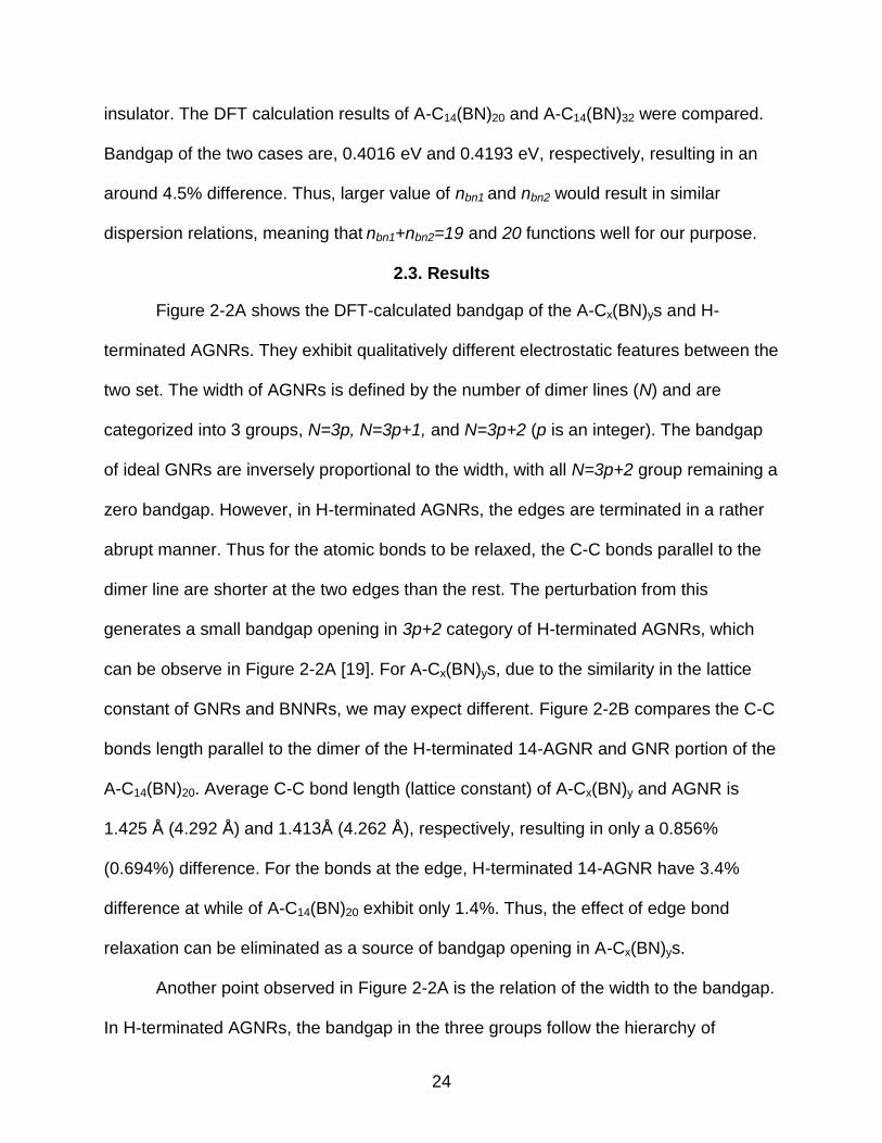
2.3. Results
Figure 2-2A shows the DFT-calculated bandgap of the A-Cx(BN)ys and H-
terminated AGNRs. They exhibit qualitatively different electrostatic features between the
two set. The width of AGNRs is defined by the number of dimer lines (N) and are
categorized into 3 groups, N=3p, N=3p+1, and N=3p+2 (p is an integer). The bandgap
of ideal GNRs are inversely proportional to the width, with all N=3p+2 group remaining a
zero bandgap. However, in H-terminated AGNRs, the edges are terminated in a rather
abrupt manner. Thus for the atomic bonds to be relaxed, the C-C bonds parallel to the
dimer line are shorter at the two edges than the rest. The perturbation from this
generates a small bandgap opening in 3p+2 category of H-terminated AGNRs, which
can be observe in Figure 2-2A [19]. For A-Cx(BN)ys, due to the similarity in the lattice
constant of GNRs and BNNRs, we may expect different. Figure 2-2B compares the C-C
bonds length parallel to the dimer of the H-terminated 14-AGNR and GNR portion of the
A-C14(BN)20. Average C-C bond length (lattice constant) of A-Cx(BN)y and AGNR is
1.425 Å (4.292 Å) and 1.413Å (4.262 Å), respectively, resulting in only a 0.856%
(0.694%) difference. For the bonds at the edge, H-terminated 14-AGNR have 3.4%
difference at while of A-C14(BN)20 exhibit only 1.4%. Thus, the effect of edge bond
relaxation can be eliminated as a source of bandgap opening in A-Cx(BN)ys.
Another point observed in Figure 2-2A is the relation of the width to the bandgap.
In H-terminated AGNRs, the bandgap in the three groups follow the hierarchy of

25
E3p+2<E3p<E3p+1, where Ez represents the bandgap of the categorized group z. However,
A-Cx(BN)ys, follows the hierarchy as E3p+2<E3p+1<E3p. The C atoms close to the junction
will encounter perturbation of on-site energy which we expect also be the cause for
bandgap opening for 3p+2 group.
Evidence of the perturbation can be observed in Figure 2-3, which shows the
pseudo charge density of an A-Cx(BN)y and a H-terminated AGNR. For an H-terminated
AGNR, the symmetry of the charge density is preserved with only a small perturbation
at the H-terminated edge. An A-Cx(BN)y on the other hand, the charges redistribute and
populate highly at nitrogen, which is caused by the large ionic potential difference
between B and N.
For analytical purpose, we can construct an effective Hamiltonian matrix only
focusing on the GNR part of the A-Cx(BN)y structure as in the schematic of Figure 2-1B.
The difference considered for this effective Hamiltonian matrix from that of ideal AGNR,
is the perturbed potential energies on the C atoms adjacent to the B and N. Here, for
simplicity we will assume that the large absolute on-site energy of B and N will only
affect the nearest C atoms, thus total 4 atoms. We will refer the perturbed potential
energies as Ea (Eb) as perturbed by B (N). The perturbation was calculated on
equivalent two-ladder system at k=0 [19]. The bandgap for the 3p and 3p+1 category of
the A-Cx(BN)y is as in equation (2-1). Further derivation is in the Appendix A.2.
0 2 2
3 3
0 2 2
3 1 3 1
2 1 3 (2 1)2 sin ( ) sin ( )
1 3 1 3 1
1 3 ( 1)2 sin ( ) sin ( )
1 3 2 3 2
a bp p
a bp p
E E p p pE E
N p p
E E p p pE E
N p p
(2-1)

26
The Eo3p and Eo
3p+1 are the bandgap for ideal AGNR which are given by,
tCC[4cos(pπ/(3p+1))-2] and tCC[2-4cos(pπ/(3p+2))] , respectively [19]. The analytical
calculation results are included in Figure. 2-2A, marked as gray crosses. The cases for
3p+2 are not included. Due to the initial zero bandgap of the 3p+2 systems, perturbation
calculation does not hold for this category. However shows perturbation indeed affects
the bandgap hierarchy.
For better understanding the mechanism, a Tight Binding (TB) model was
conducted. Though DFT calculation provides accurate description of the system, it is
computationally expensive. The TB model is a computationally cost effective method,
which can facilitate further device studies. The Hamiltonian of this model can be
expressed as equation (2-2) and the values of the parameters used are listed in Table
2-1.
0
,
, ,
( ) ( ) 'i i i i i j j i i i j j i C i
i i j i j i
H c c t c c c c t c c c c E
(2-2)
Indices i and j denote the site, ci+ and ci are creation, annihilation operators.
Also,
: Site Energy of Boron
: Site Energy of Nitrogen
: Site Energy of Carbon at sublattice A
: Site Energy of Carbon at sublattice B
BN
BN
i
CC
CC
,
: B to N bonding parameter
: C to C bonding parameter
: B to C bonding parameter
: N to C bonding parameter
BN
CC
BC
i
NC
t
t
t
t
t

27
.
The 1st and 2nd nearest tight binding parameters were introduced for better fitting. Also,
potential changes in the confined GNR portion due to the adjunct B and N atoms were
considered, as in the previous analytic calculations. Because the TB model is
constructed within the unit cell of the system, we assumed that the potential would
effectively influence nearby atoms only in lateral direction, as indicated in Figure. 2-1C.
The fourth term in the RHS of equation (2-2) represents the changes in potential profile
at the atomistic sites. Where the value of E’C,i , is 0 for ABNNR part and denotes the
decaying potential from the B or N atoms affecting the nearby C atoms, which can be
expressed as equation (2-3) in the AGNR part.
,' ( ) ( )C n B NE V n V n (2-3)
/( ) B Cnd
B B BNV n P e
(2-4)
/( ) ( ) N Cnd
N N BNV n P e
(2-5)
In equation (2-4) and (2-5), the potential is defined in exponential manner, where,
PB and PN are the strength of the potential and λ is the decay length [25]. dB-Cn (dN-Cn)
denotes distance from the B (N) at the edge to the nth C atom. Figure 2-4A plots the
bandgap results of ab-initio calculation and TB model, which fits within 6% range.
Figure 2-4B depicts few of the resulting dispersion relations in the region of interest.
Thus the TB model employing potential changes in the AGNR portion of A-Cx(BN)ys
describes the system well. Figure 2-4C shows the extended TB calculation. Although
,2
,2
0
: 2nd nearest B to N bonding parameter
: 2nd nearest C to C bonding parameter
: 2nd nearest B to B bonding parameter
: 2nd nearest N to N bonding pa
BC
CC
BB
NN
i
t
t
t
t
t
,2
rameter
: 2nd nearest N to C bonding parameterNCt

28
the bandgap is inversely proportional to the width for both cases, the minimal bandgap
of A-Cx(BN)ys’ is considerably larger than that of H-terminated GNRs. Both TB
calculation and analytic calculation match.
2.4. Summary
We have investigated electronic properties of A-Cx(BN)ys through DFT
calculation. The edge bond relaxation that is evident in H-terminated AGNRs has a
significantly small effect in A-Cx(BN)ys due to the similar lattice constant of two materials
and thus can act as stable passivation method. The source of considerably bandgap
opening for A-Cx(BN)ys with width index of 3p+2, and distinctive width to bandgap
relations from that of H-terminated AGNRs is evaluated by the perturbation calculation
and verifies that it originates from the change in the potential energy of the C atoms in
the AGNR edges that are adjacent to B and N. A TB model of the system was
constructed as a simple and effective method to predict the electronic properties.

29
Table 2-1. Tight binding parameters for A-Cx(BN)ys
Parameters (eV)
ΔCC ΔBN tCC tBN tBC tNC tBC,2
0.015 1.95 2.5 2.9 2.0 2.5 0
tCC,2 tBB tNN tNC,2 PB PN λ (Å)
0 0 0.15 0.59 0.75 0.68 2.1
Figure 2-1. Schematic of an A-Cx(BN)ys. A) Simulated structure of A-Cx(BN)y. x-Axis is the transport direction. B) Schematic of AGNR portion of A-Cx(BN)y unitcell. Inverted open triangle (closed triangle) represents C atom perturbed by adjacent B (N), for analytical calculation. C) Schematic of A-Cx(BN)y unit cell, B and N, affecting the potential profile of at C atomic sites within the unit cell.

30
Figure 2-2. Bandgap properties and C to C distance as a function of AGNR and A-Cx(BN)ys width. A) Bandgap (Eg) vs. width plot of the DFT calculation of AGNRs (the solid line with closed square) and A-Cx(BN)ys (the solid line with open triangle), and analytical calculations of A-Cx(BN)y (gray cross ). B) C to C distance of bonds that are parallel to the dimer line vs. the atomic indices. Data extracted from the DFT calculation of H-terminated 14-AGNR (the solid line with open square) and A-C14(BN)20 (the solid line with closed triangle). Average of the H-terminated 14-AGNR is represented as dot and A-C14(BN)20 as dash. Top panel is in absolute scale, distance unit in Å. Bottom panel is in relative scale regards to the average.

31
Figure 2-3. A Pseudocharge density plot of A-Cx(BN)y and H-terminated AGNR. A) A-Cx(BN)y. B) H-terminated AGNR. Units are in e/Å3.

32
Figure 2-4. DFT and TB model bandgap calculation comparison. A) Bandgap (Eg) of A-Cx(BN)ys’ as a function of width. The DFT calculation (solid line with closed square) and the TB model results (dashed line with open triangle) are compared. On the left y-axis is the bandgap and on the right y-axis is the relative error of the two calculations. Relative error is defined as, err(%)=(Eg,ab-intio – Eg,TB)/Eg,ab-intio. B) E-k band plots of A-C8(BN)20 , A-C9(BN)19 , A-C13(BN)19 ,and A-C14(BN)20 comparing the DFT calculations (solid line) and TB results (dashed line). C) TB calculated Bandgap

33
CHAPTER 3 PERFORMANCE PROJECTION OF GRAPHENE NANOMESH AND NANOROAD
TRANSISTORS
We examine the performance limits of the field-effect transistors (FETs) with
chemically modified graphene as the channel materials. Graphene nanoroad (XNR) and
graphene nanomesh (XNM) can be created through selective chemical modification of X
adsorbate (either H or F) on graphene, which generates a bandgap while conserving
the continuous two-dimensional atomistic layer. We adopt a ballistic transistor model,
where the band structure were calculated using the Ab intio simulations to assess the
performance of graphene nanoroad and nanomesh transistors. It is shown that array of
graphene nanoroads, defined by hydrogenation or fluorination of atomically narrow
dimmer lines in a 2D graphene, are most ideal for transistor channel material in terms of
delivering a large on-current, which significantly outperforms Si metal-oxide-
semiconductor (MOS) FETs. Alternatively, comparable performance to silicon can be
achieved by careful designed graphene nanomesh through patterned hydrogenation or
fluorination. As for the chemical modification, both hydrogenation and fluorination leads
to similar transistor performance, with fluorination more preferred in terms of chemical
energetics.
3.1. Overview
Graphene, a material with high mobility, has been extensively explored for
electronics applications [32,33]. However, due to its honeycombs structure, the material
innately suffers from zero bandgap. Thus, employing pristine graphene as a channel
material in the field-effect-transistor (FET), result in a low ION/IOFF ratio. This imposes a
major obstacle for using graphene in future digital electronic device applications. To
address this problem, few ways have been proposed to induce bandgap in graphene.

34
For example, in graphene nanoribbons (GNRs) the confinement of the wave functions
tunes the electronic properties, resulting in a bandgap [34,35]. Similarly, the graphene
nanomesh or antidot, a two-dimensional (2D) graphene with nanoscale array of holes,
has also been proposed [9-11]. However, all these structures have abrupt C-C bond
terminations at the edges, and hence the atomistic control is crucial for reliable
performance. At current status, the fabrication of such precisely defined edge is still
unreliable. A bandgap can also be induced by introducing chemical modification, such
as hydrogenation and fluorination, to the graphene. These modifications alter the initial
sp2 hybridization to sp3, which induces a bandgap of a few eV in graphane or fluorinated
graphene [36-39]. The combination of the two mentioned methods has been proposed
and investigated by Singh et al [40].
Graphene-nanoroad (XNR, X denotes the type of adsorbate, i.e. H or F) is a
narrow graphene strip, similar to the GNR, sandwiched in-between two hybridized
graphenes. The hybridized graphenes confine the electron within the XNR, giving rise to
a finite bandgap. Arrays of XNRs provide a natural way of realizing a densely packed
parallel semiconductor with potentially uniform edge orientation. Applying the same idea
to antidot systems, we propose a structure with vacancy replaced by selective chemical
modification of graphene. We denote this as graphene-nanomesh (XNM). Note that,
both XNR and XNM are formed by selective chemical modifications, without breaking
the covalent C-C bonds. Thus, these structures have continuous carbon 2D atomistic
layer, in which the excessive edge-defects can be prevented.
In chapter, we evaluate the performance of FETs using the XNRs and XNMs as
the channel materials. Our results indicate that array of XNRs, which behave as densely
35
packed current paths defined by hydrogenation or fluorination functionalization, can
outperform Si metal-oxide- semiconductor (MOS) FETs. Both the hydrogenation and the
fluorination structure exhibited similar performance, even with atomistic narrow
separation. On the other hand, XNM exhibits similar performance to that of Si.
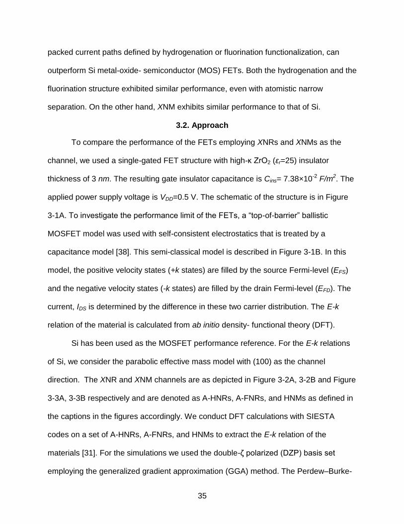
3.2. Approach
To compare the performance of the FETs employing XNRs and XNMs as the
channel, we used a single-gated FET structure with high-κ ZrO2 (εr=25) insulator
thickness of 3 nm. The resulting gate insulator capacitance is Cins= 7.38×10⁻² F/m2. The
applied power supply voltage is VDD=0.5 V. The schematic of the structure is in Figure
3-1A. To investigate the performance limit of the FETs, a “top-of-barrier” ballistic
MOSFET model was used with self-consistent electrostatics that is treated by a
capacitance model [38]. This semi-classical model is described in Figure 3-1B. In this
model, the positive velocity states (+k states) are filled by the source Fermi-level (EFS)
and the negative velocity states (-k states) are filled by the drain Fermi-level (EFD). The
current, IDS is determined by the difference in these two carrier distribution. The E-k
relation of the material is calculated from ab initio density- functional theory (DFT).
Si has been used as the MOSFET performance reference. For the E-k relations
of Si, we consider the parabolic effective mass model with (100) as the channel
direction. The XNR and XNM channels are as depicted in Figure 3-2A, 3-2B and Figure
3-3A, 3-3B respectively and are denoted as A-HNRs, A-FNRs, and HNMs as defined in
the captions in the figures accordingly. We conduct DFT calculations with SIESTA
codes on a set of A-HNRs, A-FNRs, and HNMs to extract the E-k relation of the
materials [31]. For the simulations we used the double-ζ polarized (DZP) basis set
employing the generalized gradient approximation (GGA) method. The Perdew–Burke-

36
Ernzerhof (PBE) exchange-correlation functional is adopted and the Troullier–Martins
scheme is used for the norm-conserving pseudopotentials. A grid cutoff of 300 Ry is
used and the Brillouin zone sampling is done by the Monkhost pack mesh of k-points
(31×11×1) for A-XNRs and (31×31×1) for XNMs.
3.3. Results
3.3.1. DFT Results : E-k Dispersion Relation
We first examine the E-k relation of the XNR arrays. Figure 3-2C shows 2D E-k
dispersion relations of the A-HNR{9,3} obtained from the DFT calculation. The Brillouin
zone is indicated by the red rectangle in the center. The A-HNRs have a small effective
mass along the transport direction (mt) and a large effective mass in the width direction
(ml), resulting in a highly anisotropic E-k relations. This highly anisotropic E-k relation,
would maximize both the band-structure-limited velocity in the transport direction and
the 2D density of states (DOS), simultaneously, ideal for improving transistor
performance. Figure 3-2D compares the E-k dispersion relations of the A-HNRs{9,Na},
with Na of 1, 3 and 5. The results are plotted along Y-Г-X band lines in the Brillouin
zone. Notice that the x-axis is not in scale but normalized to the Y-Г and Г-X directions.
As shown in Figure 3-2D, the slope (which represents the group velocity, vg) of the
lowest conduction band in the Y-Г direction is negligibly small, compared to that of the
Г-X direction. Even for Na of 1, isolation in transverse direction is achieved. The
bandgap of few other samples of A-HNRs with varying Ng and Na are plotted in Figure
3-2E. The Na is set to 1 or 2, 3 or 4, and 5 or 6, depending on the width of the
chemically modified portion, such that the total unitcell is an even dimer-line structure,
i.e. Na+Ng is even. This enables the unit cell to be replicated along the y-direction for
DFT calculations. The plot indicates that for the Ng=3p and 3p+1(p is an integer)

37
groups, the bandgap values remain considerably high even with one atomistic line
separation. This confirms that the atomistic chemical modification provides sufficient
confinement to the system, resulting in A-HNRs functioning similar to armchair GNRs
(AGNRs).
The inset of Figure 3-2E shows the effective mass along the transport direction
mt as a function of Ng. The mt of A-HNR{9,Na} and A-HNR{12,Na} is smaller than that of
A-HNR{10,Na}, as well as the transverse effective mass of Si, which is 0.19m0. A small
effective mass along the transport direction is preferred for a larger carrier injection
velocity and faster transistor intrinsic speed.
Next we examine the band structures of XNMs. The structure of a XNM is
illustrated in Figure 3-3A. The XNM consists of periodic arrangement of chemically
modified pattern. We consider only the modified pattern that result in hexagonal pattern
with six C and H atoms. We define this structure by the distance between the
neighboring chemically modified hexagons, which is refered to as nanoneck.
Furthermore, only the even indexed structures are taken into account, since the
bandgap of the odd indexed structures is zero [11]. The unitcell of the XNM is shown in
Figure 3-3 B. The symmetry of the unitcell provides clear definition of nanoneck and
also efficiency in DFT calculation.
Figure 3-2C, 3-2D shows the band structures of HNM{1,2} and HNM{1,6},
obtained from the DFT calculations. In the 2D gaphene, the Dirac-cone lies in the K and
K’. However, in HNMs, the shape of the super-lattice causes the Brillouin zone folding,
and thus resulting in a direct bandgap at Γ point. The two lowest conduction bands
shares the same minimum point, located at the Г point. These bands separate with

38
increasing |k|, similar to the light hole band and heavy hole band in Si. We denote the
two conduction band as the light electron (LE) and the heavy electron (HE) band. The
extracted effective mass of both the LE and HE bands are shown in the inset of Figure
3-3E. The narrower nanoneck induces stronger quantum confinement to the system and
as a result, the bandgap decreases with increasing W. In general, the HNMs introduce
sufficient bandgap in the graphene system. However, due to its nearly isotropic E-k
relation with a larger effective mass, HNM are less advantages compared to A-HNRs in
terms of carrier transport.
3.3.2. DFT Results : Binding Energy Calculation Using Basis Set Superposition Error (BSSE)
In the earlier work, schemes of hydrogenation and fluorination on carbon system
have been studied, and it was suggested that fluorination is energetically more
preferred and easier to be achieved [39]. We confirm the argument by calculating the
binding energy of the A-HNRs and A-FNRs by the DFT calculation.
SIESTA, a DFT calculation code used in this work utilizes localized pseudo-
atomic-orbital (PAO) basis. However, it is well known that in calculating binding energy
of two systems, the PAO basis set may generate error. The unequal basis set between
interacting bonded system and non-interacting separate system gives over-estimation.
This is known as basis set superposition error (BSSE), and need to be compensated
for. Detail of the method is in appendix B.
Figure 3-4 compares the C-H and C-F binding energy of the A-HNRs and A-
FNRs as a function of width of the AGNR portion (Ng). The Na is set a 3(4) for odd
(even) Ng to set the width of the whole unitcell as even for simulation purpose. Notice
that C-F binding energy is ~1.2 eV larger than C-H. Thus, we conclude that the

39
fluorination is advantageous over hydrogenation in terms of fabrication and structural
stability, without sacrificing the performance as we will demonstrate in the Chapter
3.3.3.
3.3.3. Device Performance
Next we study the ballistic performance of the MOSFET devices using XNMs and
XNRs as the channel. We apply the top-of-barrier model to the E-k dispersion relations
calculated from DFT. The performance of the MOSFETs using the A-HNRs (HNMs), as
is compared to Si, is shown in Figure 3-5 (Figure 3-6).
Figure 3-5A shows the I-V characteristic of the A-HNR FETs. For a fair
comparison of the on-current (ION), we adjust the gate workfuntion such that the off-
current density (IOFF) is set to 100nA/µm for all the MOSFETs. The A-HNR FETs with an
index of {9,3} or {12,4} offer the largest ION. Especially, A-HNR{12,4} MOSFET show
52.4% larger ION compared to the Si-MOSFET. Since we have adopted a ballistic
transistor model to evaluate the performance of the channel materials, the current is
calculated as product of vavg and number of mobile carriers that are at the top of the
barrier. As shown in Figure 3-5B, at a fixed gate bias of VG=0.5V, vavg of A-HNR{12,4}
MOS-FET is 82.9% higher than Si MOSFET, resulting in a larger ION. The larger vavg in
A-HNR{9,3} and A-HNR{12,4} is due to the large ml, as mentioned previously. The solid
lines with closed polygon in the Figure 3-5B are thermal velocity of the carriers
expressed as equation (3-1).
2 BT
t
k Tv
m (3-1)
The, kB is the Boltzmann constant and T=300K. The analytic values and the
numerical results match well in the low VG range at the non-degenerate limit. The ION is
40
the product of the charge density and the average velocity. It has been reported before
that a smaller effective mass in an isotropic E-k does not necessarily leads to a larger
on-current, because increase of the carrier injection velocity can be offset by decrease
of the density-of-states (DOS)[42]. A small effective mass along the transport direction
(for a larger carrier injection velocity) and a large effective mass in the transverse
direction (for a high DOS) are most ideal, which require a highly anisotropic 2D E-k.
We also compared the intrinsic speed of the FETs, using the intrinsic delay,
( ) /ON OFF ONQ Q I . This serves as a fair comparison metric in that it takes account of
both ON state and OFF state of the device, and also the power supply voltage. The
details of the method to compute the intrinsic delay are delineated in ref. 43. The
calculated results are shown in Figure 3-5 C, which indicate that, at a common on-off
ratio of 103, A-HNR{12,4} is two times faster than Si. This is caused by the larger
average carrier injection velocity in A-HNR{12,4}.
Figure 3-6 shows performance limits of HNMs compared to that of Si. The
modeled HNM{1,2} and HNM{1,4}, whose bandgaps are larger than 0.7 eV exhibit
comparable performance to Si, but are less preferable than A-HNRs with Ng=3p+1
category. The main limiting factor in the HNMs, is the large effective mass in the
transport direction, which lowers the carrier injection velocity. The extracted effective
mass for HNM{1,4} is 0.15m0 for LE band and 0.17m0 for the HE band. Even though the
effective mass in HNM can be further decreased by increasing the nanoneck (Figure 3-
3E), this would also decrease the bandgap, thus limit the achievable maximum on-off
current ratio.

41
Finally we further investigate the performance of HNRs as shown in Figure 3-7.
First, we study the effect of varying separation (Na) of HNRs, on the device
performance. Referring to Figure 3-7A, at VG of 0.5 V, comparing A-HNR{9,1} and A-
HNR{9,3}, the current show a difference of less than 5% and vavg show a difference of
12.5%. Thus we can verify that even one atomistic dimer-line separation generated by
chemical modification can offer enough isolation and provide comparable performance
to those of large Na. Second, we compare the effect of hydrogenation and fluorination of
HNRs, by comparing the performance of A-HNRs and A-FNRs. Referring to Figure 3-
7A, and 3-7B, A-HNR{9,3} and A-FNR{9,3} show close performance resemblance, only
2% difference in ION, and 3% in vavg. The summary of the performance of each device is
compared with Si in Table 3-1.
3.4. Summary
The electronic properties of selectively chemical modified XNRs and XNMs were
evaluated using Ab initio calculations. For XNRs, a considerable band gap comparable
to AGNR of the same confinement width can be achieved even with a single atomistic
line of hydrogenation or fluorination in a 2D graphene sheet. Hydrogenation and
fluorination leads to similar transistor performance, with fluorination more preferred in
terms of chemical energetic. The ballistic performance limits of devices using XNRs and
XNMs as channel were investigated using a top-barrier method. Due to high anisotropic
feature of the E-k relations, the performance of XNR transistors is better than that of
XNM transistors. A carefully defined pattern of the selective chemical modification to the
graphene system is promising in achieving high on-off ratio and speed, which are
required in digital electronic device applications.
42
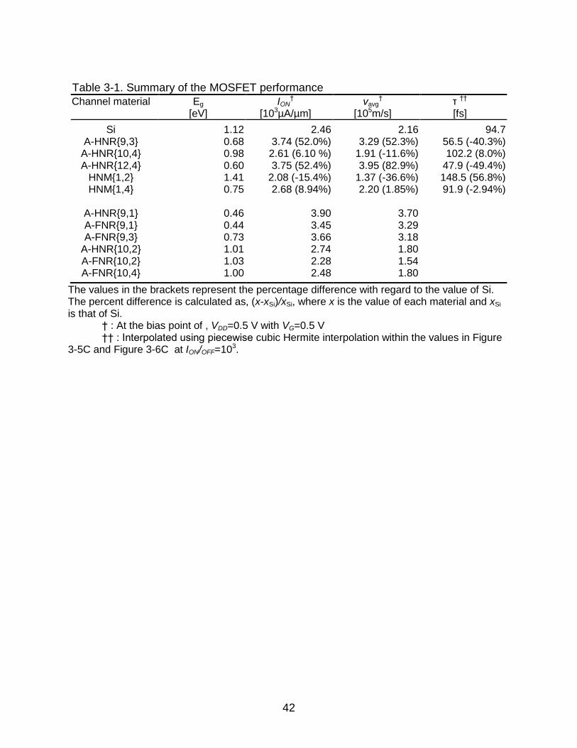
Table 3-1. Summary of the MOSFET performance
Channel material Eg [eV]
ION†
[103µA/µm] vavg
† [105m/s]
τ †† [fs]
Si 1.12 2.46 2.16 94.7 A-HNR{9,3} 0.68 3.74 (52.0%) 3.29 (52.3%) 56.5 (-40.3%)
A-HNR{10,4} 0.98 2.61 (6.10 %) 1.91 (-11.6%) 102.2 (8.0%) A-HNR{12,4} 0.60 3.75 (52.4%) 3.95 (82.9%) 47.9 (-49.4%)
HNM{1,2} 1.41 2.08 (-15.4%) 1.37 (-36.6%) 148.5 (56.8%) HNM{1,4} 0.75 2.68 (8.94%) 2.20 (1.85%) 91.9 (-2.94%)
A-HNR{9,1} 0.46 3.90 3.70 A-FNR{9,1} 0.44 3.45 3.29 A-FNR{9,3} 0.73 3.66 3.18
A-HNR{10,2} 1.01 2.74 1.80 A-FNR{10,2} 1.03 2.28 1.54 A-FNR{10,4} 1.00 2.48 1.80
The values in the brackets represent the percentage difference with regard to the value of Si. The percent difference is calculated as, (x-xSi)/xSi, where x is the value of each material and xSi is that of Si.
† : At the bias point of , VDD=0.5 V with VG=0.5 V †† : Interpolated using piecewise cubic Hermite interpolation within the values in Figure
3-5C and Figure 3-6C at ION/OFF=103.

43
Figure 3-1. Schematic of the device structure and the top-of-barrier ballistic transistor model. A) Schematic of device structure. Single top gated MOSFET with high-κ ZrO2 (εr=25) insulator with thickness of 3 nm. Cins= 7.38×10⁻² F/m2, VDD=0.5 V B) Schematic of “top-of-barrier” ballistic transistor model. The +k states are filled by the source Fermi level (EFS) and the -k states are filled by the drain Fermi level (EFD).

44
Figure 3-2. Schematic of the graphene Nanoroad and the bandgap properties. A) Graphene Nanoroad array. B) Atomistic structure of the Armchair Nanoroad. The unit cell of the 2D structure which is denoted as A-XNR{Ng,Na}. Ng is the number of dimer lines of the graphene portion and Na is the number of dimer lines of chemically modified graphene. The Ng=9, and Na=3 for this case. X denotes the adsorbate (i.e. H or F). C) The 2-D band structure of A-HNR{9,3}. The red dash rectangle is the Brillouin zone. D) E-k relation of A-HNR{9,Na} along the Y-Г-X band lines in the Brillouin zone with varying Na. Notice that the x-axis is not in scale but normalized for Y-Г and Г-X direction. E) The bandgap as a function of the Ng for a few different Na values. Na is 1 or 2 (solid line), 3 or 4(dashed line), and 5 or 6 (dotted line), depending on the width of the chemically modified portion. The inset shows the effective mass in the transport direction (mt) as a function of Ng.

45
Figure 3-3. Schematic of the graphene nanomesh and the bandgap properties. A) Atomistic structure of the nanomesh, which is denoted as XNM{R,W}. R, fixed to 1 lattice constant throughout the work, is the radius of the selectively chemical modified graphene portion. W is the width of the graphene nanoneck between two neighboring selectively chemical modified graphene. X denotes the adsorbate i.e. H. The structure shown here is HNM{1,4}. B) The unit cell of the 2D nanomesh superlattice structure. Band structure of C) HNM{1,2}, and D) HNM{1,6}. The red dash hexagon is the Brillouin zone. E) The bandgap as a function of W. The inset shows the electron effective masses of the structure. LE (HE) stands for light electron (heavy electron) band effective mass.

46
Figure 3-4. C-H and C-F binding energy of A-XNR structures with Na=3 or 4. The results are from DFT calculations. The figure indicates that C-F bonding is more energetically favorable than C-H bonds.
Figure 3-5. The ballistic performance limits of Graphene nanoroad FETs compare to Si. A common off current density of 100nA/µm is defined by adjusting the gate workfunction for all transistors for a fair comparison of the ION. A) The IDS vs. VG characteristics are compared to that of Si MOSFETs. B) Average carrier injection velocity (vavg) as a function of the gate voltage for graphene nanoroad FETs. The solid lines with closed polygons are thermal velocity. C) Intrinsic transistor delay vs. on-off current ratio where the channel length was assumed as 22nm. The detailed method is described in [14].

47
Figure 3-6.The ballistic performance limits of Graphene nanomesh FETs compare to Si and GaAs. A) The IDS vs. VG characteristics. B) Average carrier injection velocity (vavg) as a function of the gate voltage for graphene nanomesh FETs. The solid lines with closed polygons are the thermal velocities. C) Intrinsic transistor delay vs. on-off current ratio where the channel length was assumed as 22nm
Figure 3-7. A-HNRs and A-FNRs device performance comparison A) Comparison of ID vs. VG characteristics of A-HNRs and A-FNRs. B) Average carrier injection velocity (vavg) as a function of the VG for A-HNRs and A-FNRs.

48
CHAPTER 4 n-DOPING OF TRANSITION METAL DICHALCOGENIDES BY POTASSIUM
Potassium (K) has a small electron affinity and thus is acts as a strong electron
donor, however, its high reactivity impairs it stability as a dopant in graphene. Transition
metal dichalcogenides (TMDs) are a new material of interest due to its atomistic
thickness and nominal bandgap. Ab initio simulations were performed to understand K
doping of MoS2 and WSe2 in comparison with graphene. The results indicate that K
dopant in MoS2 or WSe2 induce larger charge transfer compared to K dopant in
graphene. Also the binding energy of the K to the MoS2 and WSe2 is larger than K to
graphene indicating that the K acts as more stable dopant in the TMD system.
4.1. Overview
The first demonstration of graphene [7] unveiled a class of 2D layered material to
the palette of future nano-devices. Such material includes h-BN, topological insulators,
and transition metal dichalcogenides (TMDs). Graphene has been of a great interest
due to its fascinating properties such as mobility in the order of 105 cm2/V.s, thermal
conductivity up to 3000 W/K.m [48,49]. However, due to the absence of band gap, the
graphene-based field-effect transistors (FETs) have high off-current (IOFF) and thus is
not suitable for current logic applications. On the contrary the h-BN, has large direct
bandgap of 5.9 eV which makes it appropriate for optoelectronic applications [50,51],
but rather too high for low power device applications. The TMDs, e.g., MoS2 and WSe2
are also layered 2D material with crystal structure built up of X–M–X monolayers
(M=Mo, W; X=S, Se). Each layer is interacted through van der Waals force. Previous
research reports that TMDs have a nominal bandgap of 1.1–2 eV [52,53], which is
comparable to Si, and thus it is a promising candidate for future nano-electronics.

49
Recent study of monolayer and few layered MoS2, which has a bandgap of ∼1.8 eV,
has shown the potential use high performance n-type FETs (n-FETs) [13]. Another
study has shown WSe2, which has a bandgap of ~1.2 eV, used as p-type FETs with
doped source and drain [55]. Also theoretical studies show promising results on
adapting TMDs as a channel material [56,57]. Motivated upon these studies, we focus
on understanding the doping of monolayer (ML) of MoS2 and WSe2, in particular, n-type
doping with potassium (K). K has small electron affinity and thus is acts as a strong
electron donor. K doping in graphene has already been studied in depth and the high
reactivity of the dopant make it less practical and this is illustrated by the need of
cryogenic temperatures and ultra high vacuum conditions to stably adsorb potassium on
graphene surfaces [58]. Our question is would K serve as decent n-type dopant in TMD
system and if it does, why.
In this chapter we compare the doping nature of graphene, monolayer (ML)-
MoS2 and ML-WSe2 with potassium as a dopant. Ab initio DFT simulations were
performed to understand the charge transfer and doping mechanism. Our results
indicate that the potassium has stronger interaction with the TMDs compare to
graphene. In both the K-doped MoS2 and the K-doped Wse2, the K to the neighboring
chalcogen atom bond distance was shorter than the K-C bond distance of K-graphene.
We can infer that the K doping in TMD system to be more stable than the case for
graphene.
4.2. Method
We have conducted two sets of ab-initio DFT calculation by varying the density of
K dopant atom in graphene, ML-MoS2 and ML-WSe2 system. The unitcell of graphene
consists of two C atoms, namely A, B sublattice. For the TMDs the unitcell consists of

50
one transition metal atom and two chalcogen atoms. For simulation purpose we group
the 2×2 unitcell of graphene with one K dopant (one side doping of 1/4 K atom per
unitcell) and refer it as 0.25K/UC graphene and 3×3 unitcell of graphene with one K
dopant as (1/9 K atom per unitcell) and refer it as 0.11K/UC graphene and applied the
same notation for the TMDs. Figure 4-1A shows the 2D array of 0.25K/UC of graphene,
where the supercell is depicted within the red dotted rhombus. Figure 4-1C shows that
of the TMDs. In Figure 4-1E, the supercell of 0.25K/UC TMDs is depicted for
clarification in the definition of the supercell. Figure 4-1F is the schematic for the
0.11K/UC TMDs supercell. The simulation was conducted by density-functional theory
(DFT) with Vienna ab-initio simulation package (VASP) codes [59]. Compare to SIESTA
codes [31], the VASP simulator uses atom-independent basis set to solve the Kohn-
Sham equation. Meaning that, the VASP calculation does not need compensation for
the BSSE that occurs in atom-centered basis set. Thus, to extract the binding energy of
the dopant to the 2D materials 2 sets of DFT calculation is needed. For example binding
energy of K to graphene, one calculation for K doped graphene and one for K with
graphene but distance is far enough that they will not interact with each other. The
extracted binding energy would be total energy of the first calculation subtract the value
of the second.
The double-ζ polarized (DZP) basis set was used employing the generalized
gradient approximation (GGA) method. The Perdew-Burke-Ernzerhof (PBE) is used for
the exchange-correlation potential. The cutoff energy for the wave-function expansion is
set to 500 eV. Bader analysis [60-62] was followed by the DFT calculation to
understand the charge contribution from the potassium dopant.

51
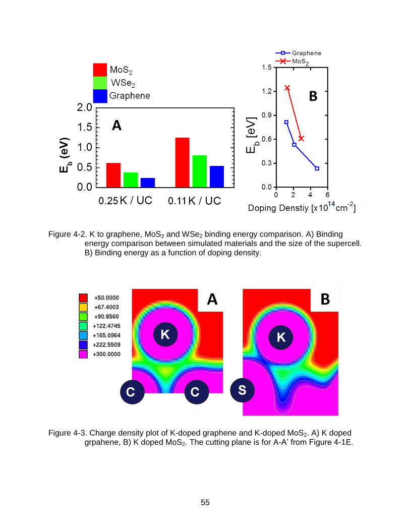
4.3. Results
For both the graphene and the TMDs, the K dopant is located above the centers
of the hexagons lattice. Figure 4-1A and 4-1B (Figure 4-1C and 4-1D) depicts the top
and side view of K-doped graphene (ML-TMD), respectively, with one-side doping and a
density of 1/4 K atom per unitcell (0.25K/UC). Despite of S being a much larger atom
than C, the distance between the K dopant and the S plane in MoS2 (2.60 Å) is shorter
than that between K and C plane in graphene (2.89 Å). The bond length of K-S is 3.06 Å
in MoS2, compared to the K-C bond length of 3.24 Å in graphene. The shorter bond
length indicates a stronger binding of K to MoS2, which is consistent with a larger
binding energy in K-doped MoS2 and more stable doping as shown in Figure 4-2A. The
results are also summarized in Table 4-1. The simulation results indicate that the bond
length decreases and the binding energy increases as the doping density decreases
from 0.25K/UC to 0.11K/UC, but the qualitative difference between K-doped MoS2 and
K-doped graphene remains unchanged. Until now we have discussed in terms of doping
density per unitcell, which may be misleading in that the size of the unitcell are rather
different. Lattice constant of graphene is 2.46 Å and MoS2 is 3.16 Å, 1.28 times larger,
and 1.64 time larger in terms of area. For a fair comparison, Figure 4-2B plots the
binding energy as function of doping density. The binding energy of the K to MoS2 is still
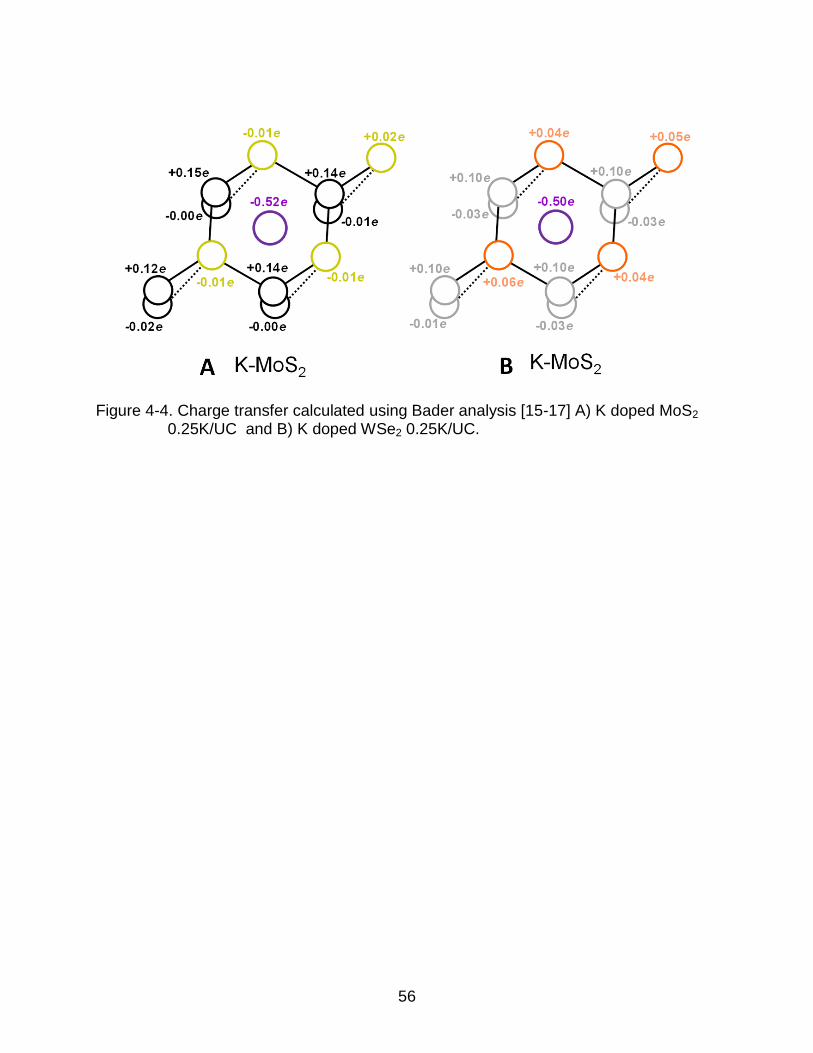
larger than K to graphene. Figure 4-3 plots the charge density distribution of K doped
graphene and K doped MoS2, where the cutting plane is shown in Figure 4-1E. For K
doped MoS2 system, we can confirm the larger interaction between the S atom to K
compare to C-K interaction in K doped graphene. We also performed similar simulations
of K-WSe2. The distance between the K dopant and the Se plane is 2.76 Å and the K-Se
bond length is 3.36 Å. Because WSe2 have larger atoms than MoS2, the bond length is

52
larger and the binding energy is smaller, but the K-WSe2 binding energy is still larger
than that of a K-graphene.
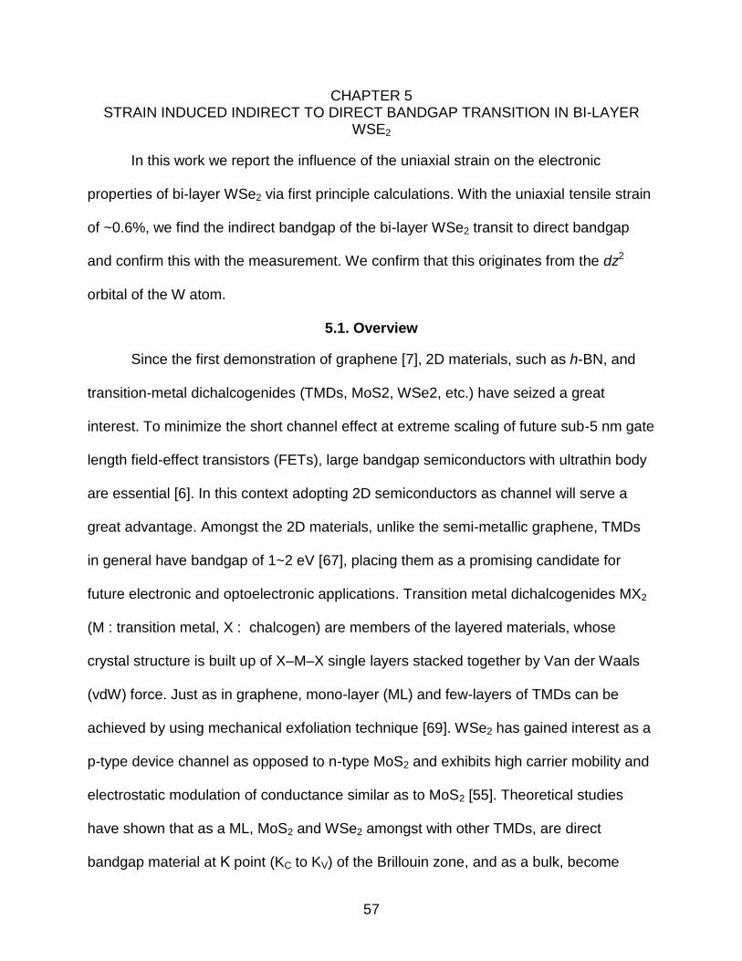
To examine charge transfer between the K dopant and the ML 2D materials, we
performed Bader analysis of charge transfer as shown in Figure. 4-4, with a K
concentration of one atom per four MoS2 unit cells (0.25K/UC). After placing one K atom
in the center of the super cell, there is 0.52e of charger transferred from the K atom to
MoS2, with the top atoms on the top S layer sharing the charge, while in ML WSe2, 0.50
of the K charge is transferred, slightly lower than that of K-MoS2’s.
4.4. Summary
In this chapter, we have studied the potassium n-doping of ML-TMD and
compared with the graphene through DFT calculations. The results indicate larger
charge transfer of K to TMD system then graphene when doped. Also the larger binding
energy indicates that K doping in TMD system is more stable than graphene case.
Confirming that TMDs can be doped, we may expect development of layered
semiconductor MOS devices.

53
Table 4-1. Summary of bonding properties of MoS2 and graphene
MoS2 Graphene
Eb(eV) dK-S (Å) Interlayer dist (Å) Eb(eV) dK-C(Å) Interlayer dist (Å)
0.25K/UC 0.612 3.19 2.60 0.233 3.22 2.89
0.11K/UC 1.248 3.07 2.43 0.532 3.11 2.77
0.06K/UC 0.813 2.97 2.6
54
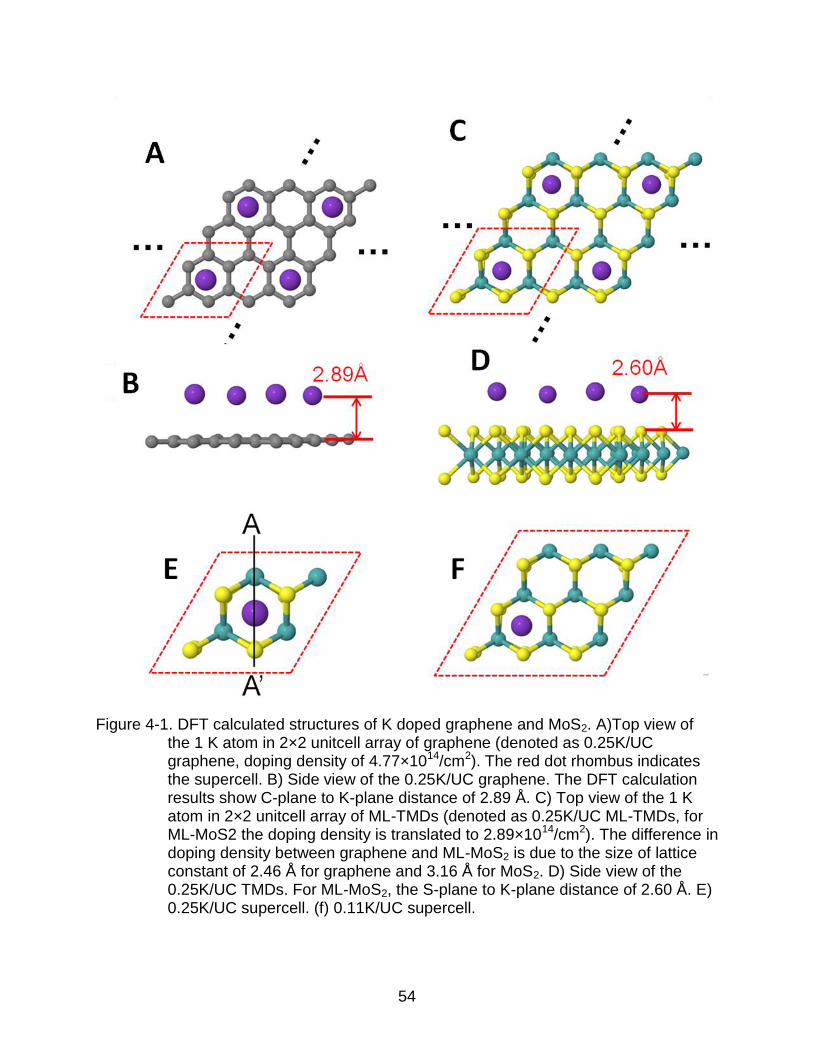
Figure 4-1. DFT calculated structures of K doped graphene and MoS2. A)Top view of the 1 K atom in 2×2 unitcell array of graphene (denoted as 0.25K/UC graphene, doping density of 4.77×10¹⁴/cm2). The red dot rhombus indicates the supercell. B) Side view of the 0.25K/UC graphene. The DFT calculation results show C-plane to K-plane distance of 2.89 Å. C) Top view of the 1 K atom in 2×2 unitcell array of ML-TMDs (denoted as 0.25K/UC ML-TMDs, for ML-MoS2 the doping density is translated to 2.89×10¹⁴/cm2). The difference in doping density between graphene and ML-MoS2 is due to the size of lattice constant of 2.46 Å for graphene and 3.16 Å for MoS2. D) Side view of the 0.25K/UC TMDs. For ML-MoS2, the S-plane to K-plane distance of 2.60 Å. E) 0.25K/UC supercell. (f) 0.11K/UC supercell.
55
Figure 4-2. K to graphene, MoS2 and WSe2 binding energy comparison. A) Binding energy comparison between simulated materials and the size of the supercell. B) Binding energy as a function of doping density.
Figure 4-3. Charge density plot of K-doped graphene and K-doped MoS2. A) K doped grpahene, B) K doped MoS2. The cutting plane is for A-A’ from Figure 4-1E.
56
Figure 4-4. Charge transfer calculated using Bader analysis [15-17] A) K doped MoS2 0.25K/UC and B) K doped WSe2 0.25K/UC.
57
CHAPTER 5 STRAIN INDUCED INDIRECT TO DIRECT BANDGAP TRANSITION IN BI-LAYER
WSE2
In this work we report the influence of the uniaxial strain on the electronic
properties of bi-layer WSe2 via first principle calculations. With the uniaxial tensile strain
of ~0.6%, we find the indirect bandgap of the bi-layer WSe2 transit to direct bandgap
and confirm this with the measurement. We confirm that this originates from the dz2
orbital of the W atom.
5.1. Overview
Since the first demonstration of graphene [7], 2D materials, such as h-BN, and
transition-metal dichalcogenides (TMDs, MoS2, WSe2, etc.) have seized a great
interest. To minimize the short channel effect at extreme scaling of future sub-5 nm gate
length field-effect transistors (FETs), large bandgap semiconductors with ultrathin body
are essential [6]. In this context adopting 2D semiconductors as channel will serve a
great advantage. Amongst the 2D materials, unlike the semi-metallic graphene, TMDs
in general have bandgap of 1~2 eV [67], placing them as a promising candidate for
future electronic and optoelectronic applications. Transition metal dichalcogenides MX2
(M : transition metal, X : chalcogen) are members of the layered materials, whose
crystal structure is built up of X–M–X single layers stacked together by Van der Waals
(vdW) force. Just as in graphene, mono-layer (ML) and few-layers of TMDs can be
achieved by using mechanical exfoliation technique [69]. WSe2 has gained interest as a
p-type device channel as opposed to n-type MoS2 and exhibits high carrier mobility and
electrostatic modulation of conductance similar as to MoS2 [55]. Theoretical studies
have shown that as a ML, MoS2 and WSe2 amongst with other TMDs, are direct
bandgap material at Κ point (KC to KV) of the Brillouin zone, and as a bulk, become

58
indirect bandgap between a local conduction band minima (CBM) near midpoint of Γ
and Κ (we will refer this as Σ point) to valence band maxima (VBM) at Γ (ΓV) [70]. The
notations ΚC, Σ, ΚV and ΓV represent the four local CBM and VBM points of the Brillouin
zone (refer to Figure 5-2C). This indirect bandgap nature of multilayer TDMs limits their
application in optoelectronic devices. One way to engineer the band structure of a
material is to apply strain. In TMDs, lattice constant and interlayer distance which is the
vdW gap, can be modified by applying strain. This results in modification of electronic
band structure, especially in the energy regions of interest: the CBM and VBM. A
dramatic transition from semiconducting to metallic with application of strain has been
reported in ML and bi-layer (BL) MoS2 by the DFT calculations [71]. In application
involving light harvesting or detection, thicker films with direct optical bandgap are
favorable. Thus, for an indirect bandgap BL or even for few-layer TMD, assuming that
the energy difference of the indirect and direct bandgap is small enough, applying strain
may lead to indirect to direct bandgap crossover. Previous study shows that the direct
and indirect bandgap difference (equivalent to KC and Σ energy difference) of BL MoS2
is relatively large, value of ~300 meV [54]. Also no transition to direct bandgap was
observed up to 2.2% uniaxial tensile strain [72]. Compared to MoS2, WSe2 BL has
smaller KC and Σ energy difference of ~40 meV. Thus, it may be possible to achieve
direct bandgap in BL WSe2 under certain strain.
In this work we present density functional theory (DFT) calculations on a BL
WSe2 to understand the effects of the strain on the band structure. BL WSe2 exhibits
indirect bandgap from Σ to KV at zero strain. As the strain is applied, we find that the KC
energy is indeed lowered while the Σ, KV and ΓV energy are relatively less perturbed. At

59
uniaxial tensile strain of ~0.6%, BL WSe2 transits to KC-KV direct bandgap which is
confirmed with the photoluminescence (PL) measurements. By further examining the
band structure of ML WSe2, we find the cause of the KC lowering in the modification of
W dz2 orbital.
5.2. Method
In this study DFT calculations were performed using the projector-augmented
wave (PAW) pseudo-potential through the Vienna Ab-initio simulation package (VASP)
[59,73]. Structure relaxation was first performed to determine the relaxed atomistic
structure in the presence of uniaxial strain, and the band structure in the presence of
strain was subsequently calculated.
For the atomic structure relaxation, generalized gradient approximation (GGA)
method was used with Perdew–Burke–Ernzerhof (PBE) exchange-correlation (XC)
functional [74]. The weak interaction of vdW force was taken account via DFT-D2
method [75]. The Brillouin-zone was sampled by the 9×9×1 Monkhorst-Pack (MH)
scheme.
As for the band calculation, GGA and local density approximation (LDA), which
are semi-local XC functionals, typically underestimate experimental bandgap [76,77].
Heyd-Scuseria-Ernzerhof (HSE) gives a larger bandgap than the LDA and GGA
simulations, but a smaller bandgap than the GW calculations [78]. It has also been
indicated that the optical gap is related to the GW bandgap subtracting the exciton
binding energy. To verify, GW quasi-particle (QP) calculation, non-self-consistent G0W0
was also performed (details can be found in the Appendix C) [79]. The band-structure
by the G0W0 calculations has an approximately k-independent shift of the conduction
bands with regard to the valence bands (0.65 eV increase between ΚC-ΚV), without

60
changing the direct or indirect bandgap feature (see Figure C.1), similar to what has
been shown before for ML TMD materials with or without strain [80]. The GW bandgap
is larger than HSE bandgaps. An exciton binding energy of about 1 eV has been
reported for ML TMD materials, but with uncertainty. The value varies by about a factor
of two if different k point grids are used in simulation [80], and it decreases by about a
factor of two from monolayer to bilayer [81]. It is also dependent on the surrounding
electrostatic environment, which is the capping PMMA and the substrate material whose
dielectric properties are not exactly clear. The uncertainty of the exciton binding energy
makes a comparison to experiment difficult. On the other hand, it is found that the PL
peak energy agrees with the bandgap of the HSE calculation with spin orbit coupling
(SOC) taken into account. This is a coincidence, which could be due to cancellation of
the blue shift by GW correction and red shift by exciton binding. Nevertheless, instead
of introduce fitting parameters for uncertainty of the exciton binding energy, the band-
structures from the HSE calculations with SOC are presented next, since we are mainly
interested in the indirect to direct bandgap transitions with the applied strain.
Thus, for band structure calculation, HSE XC potential with SOC was used with
increased k-point sampling of 15×15×1. Also as reference to the HSE results, GGA
band structure calculations were conducted (VASP input scripts in generating HSE and
G0W0 results are included in Appendix D). Figure 5-1A is the top view BL WSe2. The
arrows indicate the orientation of the applied uniaxial tensile strain. Figure 5-1B shows
the side view of the calculated structure, which the layers are in 2H stacking order.
Throughout the work, Poisson's ratio of 0.19 was used to the transverse direction of the
applied strain [67].
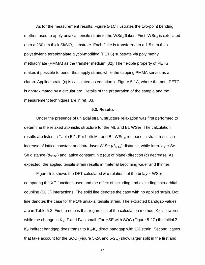
61
As for the measurement results, Figure 5-1C illustrates the two-point bending
method used to apply uniaxial tensile strain to the WSe2 flakes. First, WSe2 is exfoliated
onto a 260 nm thick Si/SiO2 substrate. Each flake is transferred to a 1.5 mm thick
polyethylene terephthalate glycol-modified (PETG) substrate via poly methyl
methacrylate (PMMA) as the transfer medium [82]. The flexible property of PETG
makes it possible to bend, thus apply strain, while the capping PMMA serves as a
clamp. Applied strain (ε) is calculated as equation in Figure 5-1A, where the bent PETG
is approximated by a circular arc. Details of the preparation of the sample and the
measurement techniques are in ref. 83.
5.3. Results
Under the presence of uniaxial strain, structure relaxation was first performed to
determine the relaxed atomistic structure for the ML and BL WSe2. The calculation
results are listed in Table 5-1. For both ML and BL WSe2, increase in strain results in
increase of lattice constant and intra-layer W-Se (dW-Se) distance, while intra-layer Se-
Se distance (dSe-Se) and lattice constant in z (out of plane) direction (c) decrease. As
expected, the applied tensile strain results in material becoming wider and thinner.
Figure 5-2 shows the DFT calculated E-k relations of the bi-layer WSe2,
comparing the XC functions used and the effect of including and excluding spin-orbital
coupling (SOC) interactions. The solid line denotes the case with no applied strain. Dot
line denotes the case for the 1% uniaxial tensile strain. The extracted bandgap values
are in Table 5-2. First to note is that regardless of the calculation method, KC is lowered
while the change in KV, Σ and ΓV is small. For HSE with SOC (Figure 5-2C) the initial Σ-
KV indirect bandgap does transit to KC-KV direct bandgap with 1% strain. Second, cases
that take account for the SOC (Figure 5-2A and 5-2C) show larger split in the first and

62
second VBM at K point, compared to the non-SOC cases (Figure 5-2B and 5-2D).
Figure 5-2E is a re-plot of SOC and non-SOC calculation using HSE XC functional,
without any strain. The band split in the VBM at Κ point is 0.65 eV for SOC calculation
and 0.13 eV for non-SOC. Because of this band split, the bandgap profile changes. To
specific, in the no strain case, the SOC calculations show Σ-KV indirect bandgap and
non-SOC Σ-ΓV indirect bandgap. This results in larger bandgap for non-SOC calculation.
Before going into the SOC effects in BL WSe2, understanding of SOC effect in ML WSe2
is required. Figure 5-5A shows the band plot of ML WSe2 with SOC taken into account.
It is well known that the broken inversion symmetry in ML WSe2 results in large spin
splitting of VBM with opposite spin moments at two K and K’ valley and are in time
reversal to each other [84,85]. Our calculation results indicate ~0.64 eV. Difference of
the split size from the past studies (0.46 eV) comes from the difference in XC function
used [84~86]. This can be confirmed by the split size in Figure 5-2A, for BL calculation
with GGA XC function shows split of 0.48 eV. Even though the value is for the BL, the
split size is known to be similar with the ML [86]. The strong SOC originates from W d
orbitals. The KC is dominated by the W dz2 orbital (which we will confirm later on), SOC
is inactive and thus, KC holds its degeneracy [87]. In the case of 2H stacked BL TMDs,
the two layers are 180 degree in plane rotated with each other. For one layer the K and
K’ valley is switched while the spin is unchanged. Thus the 2 split bands are spin
degenerate [86]. For ΓV of the ML WSe2, the time reversal symmetry which keeps the
spin degenerate. But for BL, the Pauli’s exclusion rule forces the band to split resulting
in spin degenerate to bands. Last to note is that the bandgap value from measurement
of ~ 1.52 eV fit closer to HSE results (1.585 eV) than GGA (1.188 eV) as previously
63
stated [83]. Figure 5-3A and 5-3B show the four direct and indirect KC-KV, Σ-KV, KC-ΓV,
and Σ-ΓV bandgaps as function of applied strain. The calculation results from this point
on take account of SOC. The GGA results in Figure 5-3A indicate Σ-KV to KC-ΓV, indirect
to indirect bandgap transition with extremely small window at near 1% strain of KC-KV
direct bandgap. HSE results (Figure 5-3B) is in contrast to GGA, where at strain of
~0.6% BL WSe2 transits to a direct bandgap. The difference in the two results is due to
the closer KV and ΓV energy in GGA calculation than HSE calculation. For both GGA
and HSE, it can also be seen that the Eg,KC-ΓV, decreases more rapidly than Eg,KC-KV,
which indicates that, even for HSE prediction, with much larger strain the BL WSe2 will
eventually transit to indirect KC-ΓV bandgap. Another to note is from 0% strain to the
direct bandgap transition point, the Σ-KV indirect bandgap increase. In this strain region,
Σ is the CBM, and the VBM KV is lowered in faster rate than Σ and thus the bandgap
increases. KC is also lowered with applied strain and at near 0.6%, KC becomes the
CBM, thus direct bandgap. As the KC continues to be lowered, the bandgap decreases.
Figure 5-4 is comparison of the PL measurements which are extracted from ref 83, and
the DFT calculations. Figure 5-4A shows the shift of PL peak as the strain is applied.
The PL peak is in direct relation with the bandgap of the material, and the HSE-DFT
results show close match. As DFT results predict, the PL peak increases (bandgap
increase) until strain of ~0.5% and decrease after on. Figure 5-4B shows PL intensity at
the peak which features exponential increase. More can be interpreted from the PL
amplification plot in Figure 5-4C. The PL amplification can be calculated as in equation
(5-1), where the Boltzmann approximation is used in calculating carrier concentrations.
Also we assume that there is no radiative recombination from the indirect transition (ΣC-

64
KV) and all the radiative recombination is from the direct transition (KC-KV) only. This is
reasonable given that a radiative recombination event for the indirect bandgap requires
a phonon for momentum conservation, which makes the probability of the event
negligible.
, ,
, ,
exp
PL amplification =
exp
G Direct strain
B
G Direct zero strain
B
E
k T
E
k T
(5-1)
The , ,G Direct strainE and , , G Direct no strainE are the KC-KV direct bandgap with strain and no
strain, respectively, which are from the DFT calculations. kB is the Boltzmann constant
and T is the temperature. The CB valley shifts linearly with strain, and thus the PL
amplification changes exponentially, which can be observed in Figure 5-4C. The
comparison between the two shows that the HSE-DFT predicts the actual case very
well and also confirms that the KC point indeed is lowered as the strain is applied.
As the BL Wse2 is two single layers held together by vdW force, closer
examination of ML WSe2 can reveal the origin of the KC point shift. Figure 5-5A plots the
E-k dispersion relation of the ML WSe2, with no strain and 2% uniaxial tensile strain.
Same as the BL case the KC is lowered, and thus the initial direct bandgap changes
from 1.63 eV to 1.51 eV. We can also see the increase of ΓV, however, in ML WSe2, the
ΓV is much lower than KV, and thus does not affect the bandgap transition in the range
of strain of interest. In Figure 5-5B, we can see the monotonic decrease of the direct
bandgap.
We further investigate the electronic band structure with relative contribution from
atomic orbitals. It has been reported in previously that in TMDs, d orbital in the metal

65
atom contributes largely to the lowest conduction band and highest valence band
[88,89]. Further DFT calculations on MoS2 have revealed that the at the two
inequivalent Κ and Κ’ valleys, the KV is composed by the Mo dx2−y
2 and dxy orbitals with
some mixing from the S px and py orbitals, while the KC is dominated by Mo dz2 orbitals
[88]. We may expect the similarity in WSe2. Figure 5-6A and 5-6B verifies these
previous works, where the atomic contribution of W atom and Se atom are plotted with
the size of the circles representing the contributing rate. Figure 5-6C~G shows the d
orbital contribution from W atom, namely dxy, dyz, dz2, dxz and dx
2-y
2 respectively. As
shown in Figure 5-6D and F, the dyz, and dxz play negligible role in the CBM and VBM.
The dxy and dx2-y
2 (Figure 5-6C and 5-6G) contributes to Σ and KV evenly. Most
importantly W atom dz2 (Figure 5-6E) orbital is solely responsible for KC. Another to note
is that ΓV is affected by W atom dz2 orbital too, with small contribution from Se atom.
Thus, the large increase in ΓV for ML to BL WSe2, is also caused by the modification of
W dz2 orbital. Figure 5-7 are the partial charge calculation of at each band points of
interest (KC, Σ and ΓV), to visualize the orbital characters of single states. The partial
charge is defined as partial charge density as respect to by the volume of unit cell. In
calculating the partial charge density, the weighting of the states is not in Fermi-Dirac
distribution. Rather, the occupancies of the states are set as 1.0 within the integration
energy range (indicated in the figure) and as 0.0 otherwise. Figure 5-7A and 5-7C
clearly show that the KC and ΓV are dominated by the W dz2 orbital which is in contrast
to 5-7B which confirms the in-plane dxy, dx2-y
2contribution at KV.
5.4. Summary
BL WSe2 exhibits large PL amplification when uniaxial tensile strain is applied. We
find the cause of this to be lowering of the local conduction band minima at the Κ point

66
of the Brillouin zone. Origin of this behavior is caused by the modification of dz2 orbital in
the W atom with the applied strain. At strain of ~0.6% indirect bandgap BL WSe2
transits to direct bandgap of 1.6 eV (from PL measurement) which is confirmed with
DFT calculations and PL measurements. We also find that to achieve accurate
electronic band structure, HSE exchange correlation function with account for spin
orbital coupling to be reasonable choice, which can also be used to predict the effect of
the strain.
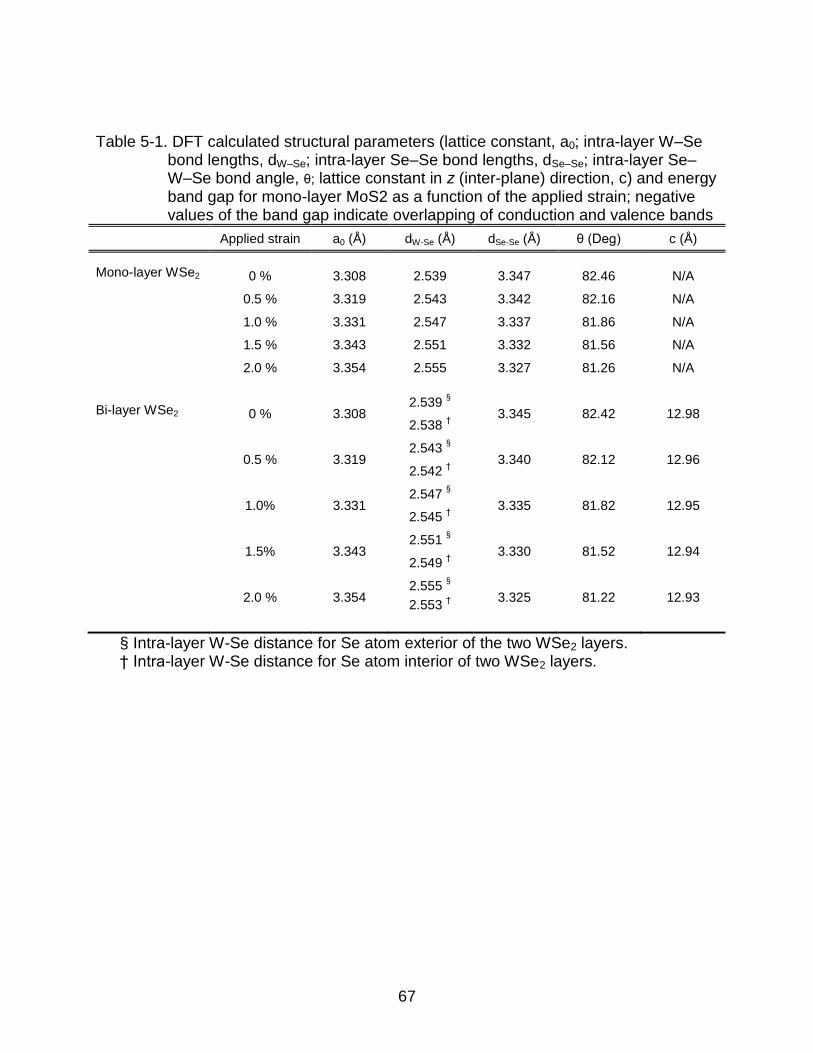
67
Table 5-1. DFT calculated structural parameters (lattice constant, a0; intra-layer W–Se bond lengths, dW–Se; intra-layer Se–Se bond lengths, dSe–Se; intra-layer Se–W–Se bond angle, θ; lattice constant in z (inter-plane) direction, c) and energy band gap for mono-layer MoS2 as a function of the applied strain; negative values of the band gap indicate overlapping of conduction and valence bands
Applied strain a0 (Å) dW-Se (Å) dSe-Se (Å) θ (Deg) c (Å)
Mono-layer WSe2 0 % 3.308 2.539 3.347 82.46 N/A
0.5 % 3.319 2.543 3.342 82.16 N/A
1.0 % 3.331 2.547 3.337 81.86 N/A
1.5 % 3.343 2.551 3.332 81.56 N/A
2.0 % 3.354 2.555 3.327 81.26 N/A
Bi-layer WSe2 0 % 3.308 2.539
§
3.345 82.42 12.98 2.538
†
0.5 % 3.319 2.543
§
3.340 82.12 12.96 2.542
†
1.0% 3.331 2.547
§
3.335 81.82 12.95 2.545
†
1.5% 3.343 2.551
§
3.330 81.52 12.94 2.549
†
2.0 % 3.354 2.555
§
3.325 81.22 12.93 2.553
†
§ Intra-layer W-Se distance for Se atom exterior of the two WSe2 layers. † Intra-layer W-Se distance for Se atom interior of two WSe2 layers.

68
Table 5-2. DFT calculated BL WSe2 bandgap
Strain XC : GGA XC : HSE
Eg [eV] Eg [eV]
SOC 0 % 1.188 Σ-ΚV 1.585 Σ-ΚV
1 % 1.210 Σ-ΚV 1.575 ΚC-ΚV
Non-SOC 0 % 1.316 Σ-ΓV 1.826 Σ-ΓV
1 % 1.305 Σ-ΓV 1.784 ΚC -ΓV
69
Figure 5-1. Schematic of bi-layer WSe2 and the mechanical strain setup. A) Schematic of bi-layer WSe2 (top view), where the arrows indicate the orientation of the applied uniaxial tensile strain. B) Side view of the bi-layer WSe2. The details of geometric parameters are in Table 5-1. C) Mechanical setup to apply strain. Arrows indicate the direction of the applied force.

70
Figure 5-2. DFT calculated E-k relations of bi-layer WSe2, comparing the XC functions and the effect of including and excluding spin-orbital coupling (SOC). The solid line denotes the case with no applied strain. Dot line denotes the case for 1% uniaxial tensile strain. A) GGA with SOC. B) GGA w/o SOC. C) HSE with SOC. D) HSE w/o SOC. Despite the method used, with applied strain, the conduction band minima at Κ point is lowered. E) Comparison of HSE-DFT calculation with and without SOC for no strain applied case.
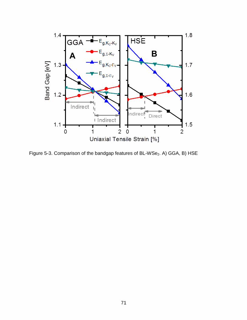
71
Figure 5-3. Comparison of the bandgap features of BL-WSe2. A) GGA, B) HSE

72
Figure 5-4. Comparison of PL measurement with HSE-DFT calculation A) PL peak energy and bandgap from DFT as function of strain. B) PL intensity at peak point vs. strain. C) PL amplification comparison between measurement and DFT calculation.

73
Figure 5-5. Bandgap features of ML WSe2. A) HSE-DFT E-k calculation of ML WSe2. B) Bandgap features as function of applied strain.

74
Figure 5-6. ML WSe2 atomic and orbital contribution on the E-k relation. A) W atom. B) Se atom. C~G are orbital contribution from the W atom dxy, dyz, dz
2, dxz and dx
2-y
2 respectively. The size of the circles is proportional to the contribution.
Figure 5-7.The partial charge calculation of at each band points of interest. A) KC, B) Σ and C) ΓV. The energy range specified in sub-figure represents the integration interval.

75
CHAPTER 6 ELECTROSTATIC SCREENING PROPERTIES OF MULTILAYER MOS2
The nonlinear electrostatic screening behavior of a multi-layer MoS2 is studied,
through numerical calculations composed of one dimensional capacitance model and
equilibrium charge statistics. We find that the electrostatic screening properties depend
highly on the applied gate voltage and the temperature. Layers of MoS2 can be
electrostatically non-screening in the insulating limit due to finite bandgap of the two
dimensional material. In the opposite limit, the screening length can be as short as half
of the interlayer distance of MoS2 layer, indicating strong screening.
6.1. Overview
Since the first demonstration of graphene in 2004 [7], the two dimensional (2D)
material has been of a great interest for the future electronic devices [92]. However, the
absence of a bandgap in the graphene results in high leakage current, i.e. low on-off
current ratio (ION/IOFF) when applied as a channel material of a field effect transistor
(FET) [32]. While there have been efforts to induce a bandgap to the semi-metallic
material, such as patterning to nano-ribbon [23,24,34], application of electric field across
few layers of graphene [93], and chemical derivatives [36] and etc., it still remains as a
challenge which force to search for alternative 2D materials. h-BN and transition metal
dichalcogenides (TMDs, such as MoS2, MoSe2, WS2, WSe2 and etc.) are a few of such.
TMDs are semiconducting layered materials, composed of vertically stacked X–M–X
layers (M=Mo,W and X=S,Se,Te) that interact through a weak van der Waals (vdW)
force. Each layer consists of a hexagonal plane of M atoms sandwiched between the
two X atom layers. As a monolayer (ML), TMDs exhibit bandgap of 1~2 eV [67]. A ML
MoS2 for example exhibits direct bandgap of 1.8 eV where, Radisavljevic et al.,[13]

76
have demonstrated a ML MoS2-based FET with a room-temperature electron mobility in
the similar range of graphene nanoribbons and a high ION/ IOFF. Fang et al.,[94] also
demonstrated n-doped MoS2 and WSe2 FETs using potassium as a dopant. Other
device topologies that adapt TMDs have been introduced. Vertical quantum tunneling
FET is one of them, which use vertically stacked TMDs together with graphene layers
[65,95,96]. In this sense, understanding of the electrostatic screening behavior of these
2D materials is crucial. Kuroda et al.[97], studied electrostatic screening features of
multi-layer graphene, where the charge density profile in each layers show non-
exponential decaying behavior. Numerical analysis showed that the screening length of
the graphene can be less than 1 layer thick to as large as few layers, depending on
screened charge density, intrinsic doping and temperature.
In this theoretical work, we use a 1 dimensional (1D) capacitance model self-
consistently iterated with the equilibrium charge calculation, to determine the
electrostatic screening behavior of few layers of MoS2. We find that the electrostatic
screening is highly nonlinear due to the 2D density of states (DOS) properties of the
MoS2. Depending on the gate bias and the temperature, the screening length can be
less than 1 layer thickness of the MoS2 and extend to infinite, meaning the insulating
limit. Also, we derive analytical expression for the Debye length which is essentially
equivalent to the screening length. Last, we compare the results with Thomas-Fermi
model and assess its validity.
6.2. Method
The studied structure is in the scheme of a FET, consisting N layers of MoS2 on
top of a SiO2 substrate with a bottom gate as in the Figure 6-1A. The equilibrium
condition is considered, thus the Fermi energy is same through the layers. The

77
interlayer coupling between the stacked layers is neglected, assuming that the layers
are stacked in an incommensurate manner. Figure 6-1B describes the 1D capacitance
model to calculate the electrochemical potential of the MoS2 layers. The numerical
calculation procedure is following that of [95] for the vertical stacking of 2D materials.
The Qi in the figure represents the charge density in the ith layer and is a function of
vacuum energy level (Evac) as in equation (6-1) for N-layer MoS2.
, 1 , 1 , 1 ,i i vac i vac i i vac i vac iqQ C E E C E E , 0,1,2...,i N . (6-1)
1 0 /ox oxC t is equivalent to the gate oxide capacitance (Cox). The dielectric
constant ( ox ) of 4 is used to represent the SiO2 gate oxide with thickness (tox) of
280nm. 0 is the vacuum permittivity. For 2i , 2,MoS 0 0/i rC d where
2,MoSr is the
interlayer dielectric constant of MoS2, and d0=6Å is the interlayer distance between the
layers. 2,MoSr is crucial in determining the charge in each layer. As the
2,MoSr in TMDs
vary with number of layer, the interpolated values from the work of Kumar et al., are
used [98]. For most part of the work, N=10 and corresponding value of 6.84 is used.
The boundaries are, C0= CN+1=0, Evac,-1=Evac,N+1=0, and eq (6-1) can be expressed as
,01 1 0
,11 1 2 2 1
,22 2 3 2
,N 11 1 1
,N
...
...... ... ... ...
vac
vac
vac
vacN N N N N
vacN N N
EC C qQ
EC C C C qQ
EC C C qQ
EC C C C qQ
EC C qQ
. (6-2)
The vacuum energy level at the gate is, ,0vac BG BGE qV , where BG is the
bottom gate work-function. The equilibrium charge density is calculated through the k∙p

78
Hamiltonian. The expression for the ith layer of MoS2 is, i i
i e hQ qn qn , where, i
en ( i
hn ) is
the electron (hole) charge density.
2
0 , 1 ,2
2
0 , 1 ,2
2 2
2
2 2
2
gi i iB Be F e F e
FF
gi i iB Bh F h F h
FF
Ek T k Tn
vv
Ek T k Tn
vv
. (6-3)
We define ,
i ii F CF e
B
E E
k T
and
,
i ii V FF h
B
E E
k T
. kB is the Boltzmann constant and
T is the temperature. i
FE are the Fermi energy levels of the ith layer MoS2 and are zero
under equilibrium state. 2MoS (5.1 eV) is the electron affinity energy of the MoS2. The
conduction band energy of ith layer is 2,
i
C vac i MoSE E and the valence band energy is
2,i
i
V vac MoS gE E E . A bandgap value ( gE ) of 1.80 eV and a Fermi velocity ( Fv ) of
5.33×10⁵ m/s is used. The corresponding effective mass is 0.52m0 for the tight binding
parameter of t0=1.1eV from the Dirac equation [84]. j is the jth order Fermi-Dirac
integral. The applied gate voltage (VG) induces 2D charge density of 0 ox GQ C V , which
depends highly upon the geometry of the gate insulator. Thus, for general quantification,
we will use quantity of gate charge density of Q0 instead of VG. Through the work, we
consider the un-doped MoS2 layers only.
6.3. Results
Figure 6-2A and 6-2B shows the charge density profile normalized by Q0, for 10
layers of MoS2 at 10K and 300 K respectively. The charge density profile features not a
simple exponential decay. The screening strength depends highly on the magnitude of
Q0 : with the larger Q0, stronger the electrostatic screening. Also at higher (away from
79
the gate) layers, the slope of the Qi/Q0 decreases, which indicates weakening of the
electrostatic screening. As shown in Figure 6-2C, the conduction band (EC) is further
away from the Fermi level (EF) in the higher layers due to the less induced electrons.
Thus, at small Q0 (for example Q0=1011cm-2 in Figure 6-2B), the screening length can
increase significantly. Temperature is also critical factor in modulating the screening
behavior. At T=300K, broadening of the Fermi-Dirac tail is larger than T=10 K. To
induce similar charge, the EC for T=300K is further from the EF then T=10K case (Figure
6-2C). Thus at larger temperature, the charge profile along the layers is more even,
than lower temperature, which implies weaker screening (i.e., longer screening length).
The electric field profile along the z-axis in Figure 6-2D confirms this temperature
dependency, where the profile at 300 K is more in an exponential manner compared to
the more radical profile at 10 K. The electric field at ith layer is calculated as equation (6-
4).
2
, 0
, 0
1 i
z i j
jr MoS
E Q Q
(6-4)
As in the previous work of screening effects in the graphene system [97], we will
use the equation (6-5) to quantify the screening strength and denote it as an effective
screening length ( , 1i i
eff ), which is determined from the charge density of a two
neighboring ith and (i+1)th MoS2 layers.
, 1 0
1
log
i i
eff
i
i
d
, 1,2..., 1i N . (6-5)
Figure 6-3A and 6-3B shows the calculated , 1i i
eff for T=10 K and 300 K,
respectively. As pointed out previously, the strength of the electrostatic screening
80
decreases (screening length increase) at higher layers, which is due to reduced induced
charge density. Also, the higher temperature results in a larger , 1i i
eff . Depending on the
Q0, the , 1i i
eff vary from less than an interlayer distance (d0) of a MoS2 to as large as
insulator limit (in given Q0 range, ~100 d0 at the bottom layer).
A Debye length ( i
D ) is a critical length which the mobile charge carriers screens
the external electric field, which is essentially equivalent to the , 1i i
eff . We will use the
Debye length at each layer to quantify the screening length and compare with the , 1i i
eff .
This can be solved with the Poisson’s equation and linearized charge density
approximation. The linearized charge calculation is derived from equation (6-3) as,
0 1 ln 1 exp
1 exp
i ii i
e iB B B
B
N NV qVn q q V
k T k T k TqV
k T
. (6-6)
The /i i i
F CV E E q , and
0 2
2
2
gB
F
Ek TN
v ,
2
1
2 B
F
k TN
v
.
As we will be dealing with n-type case only, the hole charge density, i
hn is
neglected. By self consistently calculating equation (6-6) with the 1D capacitance model
[equation (6-2)], we can find the potential iV . The analytic expression of i
D is in
equation (6-7).
0 0
0 0
2
0 2
1
1 exp
ln 1 exp
i
r B
Bi r BD i
B
qVd k T
k T d k T
q N qVq N
k T
(6-7)

81
The details of the derivation are in the Appendix E. With the limiting condition of
/ 1i
BqV k T , which corresponds to the high gate bias with high temperature condition,
the Debye length can be further simplified to
0 0
02 2
0 1
20.54
ln 2
r B r BD
k T k Td
q N q N
.
This indicates that the minimum screening length to be as short as half the MoS2
interlayer distance. Figure 6-4 shows the comparison of the two methods used to
quantify the screening length (i.e., , 1i i
eff and i
D ). Since the strength of the screening is
largest at the bottom layer, we will examine only the screening length for i=1. The plots
verify that in the case of low Q0, the screening length can extend to infinity. This
differentiates from the graphene case, where the screening length saturates to a certain
value [97]. The origin of the difference is in the bandgap. Because of the zero bandgap
property of the graphene, together with the thermal broadening of the Fermi-Dirac
charge distribution, the charge is induced even when Dirac point is at the Fermi-energy.
In turn, the induced charges partially screen the electrostatics, thus, the screening
length saturates to a temperature dependent finite value. However, this is not the case
for MoS2. The bandgap permits the layers to be non-screening, or have an infinite
screening length. The Figure 6-4 plot shows that the two models used to model the
screening length match well. Especially at higher temperature case, the range of Q0
where two plots agree is larger. This is due to the linear approximation made earlier in
calculating the charge. The linearization limits accuracy only in the range of
1 / 1i
BqV k T . With larger temperature this condition can be met with larger range
of iV , which is in direct relation with Q0. Although this study deals with multi-layer of

82
MoS2, the method used here can be adopted to any stack of 2D material with finite
bandgap.
Previous studies have successfully modeled screening behavior of graphene via
nonlinear Thomas-Fermi (TF) model [100]. Following the analytical derivation from ref.
20, we evaluate the validity of TF model by comparing with the 1D capacitance model.
The details of the derivation can be found in the reference or summary in Appendix F.
The charge density in the z (vertical) position of the thickness 0( 1)D N d system in
the continuum limit is expressed as,
0
0
0 0 0
0
0
2cosh
22
sinh
TF
z Dd
Q z Q d
Dd
, where 2
2
2
0 2
, 04
v s MoS
r MoS
e N N m
.
Figure 6-5A, compares the charge profile of 10 layer MoS2 stacks with varying Q0
using the two models. The two models only agree in small range of layer index i (or z),
at large Q0. The limitation of the analytical TF model is due to the missing bandgap
information. The derivation (see Appendix F) relies on the 2D constant DOS, and the
resulting TFQ z show exponential behavior. However, in real, there exists a bandgap in
MoS2 system where DOS becomes zero. This is evident in the conduction band (EC)
plot in Figure 6-5B. At Q0=1011 cm-2, the Fermi-level of all the layers of MoS2 are
positioned within the bandgap, thus, only the thermal broadened charges exists. This
results in large discrepancy between the two models in charge density calculation.
Likewise, even for Q0 =1013 cm-2 case, at i~3, the EC becomes larger than EF. From this
point the charge density of the 1D capacitance model saturates while the TF model
show continuous decrease.

83
6.4. Summary
In this chapter, we have investigated the electrostatic screening behavior of
multi-layer MoS2, using numerical methods accounting for applied gate voltage (or gate
charge) and temperature. The screening length of the layers depends highly on the both
variables. The major difference between multi-layer graphene is that, the graphene has
saturating screening length which is due to its semi-metallic feature. On the other hand,
MoS2, due to the sufficient large bandgap of 1.8 eV, the screening length can extend to
infinity. We also derive analytical expression for the Debye length which suggests that
the lower limit of the screening length to be around half of the interlayer distance of
MoS2 layers.

84
Figure 6-1 Schematic of multi-layer MoS2, and 1D capacitance model. A) Schematic of multi-layer MoS2, in a form of field effect transistor (FET) with a back gate. B) Corresponding 1D capacitance model of A.
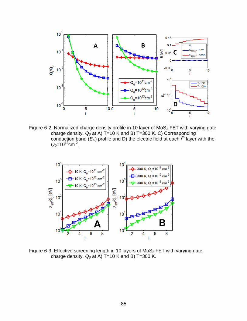
85
Figure 6-2. Normalized charge density profile in 10 layer of MoS2 FET with varying gate charge density, Q0 at A) T=10 K and B) T=300 K. C) Corresponding conduction band (EC) profile and D) the electric field at each ith layer with the Q0=1012cm-2
.
Figure 6-3. Effective screening length in 10 layers of MoS2 FET with varying gate charge density, Q0 at A) T=10 K and B) T=300 K.

86
Figure 6-4. Effective screening length between the first (bottom) two layers( i=1, λeff) compared with the Debye length (λD
i) at different temperatures.
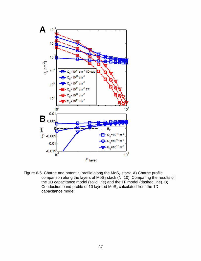
87
Figure 6-5. Charge and potential profile along the MoS2 stack. A) Charge profile comparison along the layers of MoS2 stack (N=10). Comparing the results of the 1D capacitance model (solid line) and the TF model (dashed line). B) Conduction band profile of 10 layered MoS2 calculated from the 1D capacitance model.
88
CHAPTER 7 TWO DIMENSIONAL HETEROJUNCTION DIODE AND TRANSISTOR
A vertical transistor based on a stack of atomically thin two dimensional (2D)
semiconductors is theoretically examined. The structure under study resembles that of
metal-based-transistor in that the metallic graphene is used as a base and
semiconducting MoS2 is used as an emitter and a collector. To understand the device
operating mechanism, we first investigate the properties of graphene-MoS2 junction. We
find that the characteristic of this junction depend not only on the intrinsic junction itself,
but also highly on the lateral extension region, thus detailed 2D Poisson calculation is
required for the study. As for the three terminal metal-base-transistor-like structure, the
major drawback of this structure is the large base current due to the graphene’s
excessive in-plane transport feature. This is desired in conventional lateral transport
device topologies. However, for the structure under study which utilizes the interlayer
carrier transport, the large leakage current in the base is undesired. Rather, in this type
of structure, base material with sufficient bandgpap is preferred.
7.1. Overview
Since the first demonstration of graphene in 2004 [7], the 2D material has been
of great interest for the future electronic devices [92]. However, graphene as a channel
for field effect transistor (FET) where the current path is along the in-plane direction of
the 2D material, absence of the bandgap leads to a low current on-off ratio (ION/IOFF).
This is a major obstacle in utilizing graphene as a channel material in current digital
logic applications [32]. There have been considerable efforts to induce a bandgap,
however resulted in trade off with the mobility [102,23,36]. As a contrast to the in-plane
transport of the graphene, out-plane transport properties can be exploited as

89
demonstrated by Britnell et al, using vertical stacking of 2D semiconductor materials to
create a quantum tunneling FET [65,95]. In the similar sense, graphene base hot
electron transistor (GB-HET) was proposed and explored, which show high current on-
off ratio of 104~105 [103~105]. The hot electron transistors (HETs) were introduced in
the 1960’s, where the hot electron transports from emitter to collector. The main
expectation of such device was high-speed applications due to their short base transit
time [106,107]. The GB-HETs exploits exploit this attribute to an extreme in that in that
the width of the base can be as short as single atomic thickness and the semi-metallic
property of the graphene which result in relatively low base series resistance. While the
reported structure of the GB-HETs exhibits tunneling barrier between emitter and base,
we would like to focus on a more simple structure that consists of a 2D semiconductor,
mono-layer (ML) MoS2, as a collector and an emitter and the graphene as a base. As
graphene have a semi-metallic E-k relation, this structure resembles the metal base
transistor (MBT) [108]. By adopting fabrication technique as mechanical transfer
process [64], various types of 2D material can be stacked and may expect such device
to be of low cost.
In the following chapters we will first, observe the operation principle of the metal-
semiconductor (MS) junction-like graphene-MoS2 (GM) junction. The measured I-V
curve of this 2 terminal structure show exponential behavior as expected in a MS
junction. However, the reverse bias shows non-saturating linear increase of current.
This is due to the geometry of the structure, where at the edge of the overlapping GM
junction, an extrinsic lateral tunneling path is generated. We confirm this theory with 2D
Poisson calculations coupled with the equilibrium charge calculation. We also extract
90
the graphene to MoS2 interlayer electron escape rate for transport prediction. In the
second part of this work, we focus on the MBT like structure, which is composed of two
GM junctions. Here, we consider only the intrinsic junctions to elucidate the device
mechanism. We will denote this as MoS2-graphene-MoS2 bipolar junction transistor
(MGM BJT). We find that the large base current hinders the device from achieving high
current gain. Engineering of interlayer escape rate is required and base material with
finite bandgap is preferred.
7.1. Graphene-MoS2 Junction Diode
7.1.1. One Dimensional Simulation for Vertical Junction
Figure 7-1A is a schematic of the GM junction, where the bottom MoS2 layer is
grounded and the bias (VGra) is applied to the top graphene layer. To examine the
intrinsic junction property, one-dimensional (1D) model is sufficient as in schematic in
Figure 7-1B, which can be electrostatically modeled by a 1D capacitance model as
depicted in Figure 7-1C. By solving the 1D capacitance model coupled with the carrier
statistics, potential profile can be determined. The general form to calculate the charge
at stacked system is presented in equation (7-1).
, 1 , 1 , 1 ,i i vac i vac i i vac i vac iqQ C E E C E E , 0,1,2i . (7-1)
For this case, the total number of layer is 2, where i=1 (i=2) represents the MoS2
(graphene) layer. 1 0 /ox oxC t , is equivalent to gate oxide capacitance (Cox). For the
SiO2 gate oxide, dielectric constant ( ox ) of 4 is used with thickness (tox) of 280nm. 0 is
the vacuum permittivity. 2 int 0 0/C d represents the dielectric constant between MoS2
and graphene ( int ) and is set as 1 with interlayer distance d0=6Å. The boundaries
conditions are, C0= C3=0, Evac,-1=Evac,3=0, and equation (7-1) can be expressed as [95],

91
1 1 ,0 0
1 1 2 2 ,1 1
2 2 ,2 2
vac
vac
vac
C C E qQ
C C C C E qQ
C C E qQ
(7-2).
The vacuum energy level at the gate is, ,0vac BG BGE qV , where BG is the
bottom gate work-function. This 1D electrostatic equation is self-consistently solved with
equilibrium semi-classical carrier statistics from k∙p method. The charge density of ith
layer (i=1 is MoS2 and i=2 is Graphene) is expressed as, i i
i e hQ qn qn , where,
2
0 , 1 ,2
2
0 , 1 ,2
2 2
2
2 2
2
i
gi i iB Be F e F eii
FF
i
gi i iB Bh F h F hii
FF
Ek T k Tn
vv
Ek T k Tn
vv
. (7-3)
We define1
1
,F C
F e
B
E E
k T
,
22
,F Dirac
F e
B
E E
k T
and
11
,V F
F h
B
E E
k T
,
22
,Dirac F
F h
B
E E
k T
.
kB is the Boltzmann constant and T is the temperature. 1
FE and 2
FE are quasi-Fermi
energy levels of MoS2 and graphene. When a bias of VGra is applied, they are assumed
to be separated by GraqV . The bandgap 1
gE =1.80 eV and 2
gE =0 eV for MoS2 and
graphene respectively. The MoS2 conduction band energy is 2,1C vac MoSE E and
valence band energy is 2
1
,1V vac MoS gE E E . The Dirac energy of graphene is
,2Dirac vac GraE E . 2MoS (5.1 eV) and Gra (4.5 eV) are the electron affinity energy of
MoS2 and graphene work-function, respectively. The Fermi velocity of MoS2 is 1
Fv
=5.33×10⁵ m/s and graphene is 2
Fv =1×10⁶ m/s. The corresponding effective mass for
MoS2 is 0.52m0 with tight binding parameter t0=1.1eV from the Dirac equation [84]. The
92
j is the jth order Fermi-Dirac integral. By self-consistent iteration of equation (7-2) and
(7-3), the potential the two 2D layers can be found which in turn is used to calculate the
current.
7.1.2. Classical Transport Calculation
Within the classical representation, the MoS2 and graphene interlayer tunneling
current can be expressed by the density of state (DOS) of the two materials as,
2 2
2
C MoS Gra Gra MoS
qI D E D E f E f E dE
h . (7-4)
The energy dependent DOS of MoS2, 2 2
22MoS MoSD E m (for CE E and
VE E ) and 2
0MoSD E (elsewhere), is used. The graphene DOS is
2 22gra Dirac FD E E E v and ,
2
2
1
/
/ 1 expGra MoS
Gra MoS
B
Ef
k T
.
The ML MoS2 is grounded and the bias is applied to the graphene layer thus,
20MoS and Gra GraqV . Lastly, h is the plank constant. αC is an interlayer tunneling
parameter whose value proportionally determines the interlayer transport rate and can
be extracted as a fitting factor to the experimental I-V characteristics.
The I-V of 3.3µm2 device is plotted in Figure 7-2A which is measured at 220 K
with varying back gate bias (VG). In the forward bias region, the curve exhibits
exponential behavior, however, in the reverse bias show linear current characteristic
which is not typical a typically expected in a MS or a p-n junction. The reason for this is
in the lateral extension of the junction and will be dealt in the next sub-chapter. Figure 7-
2B is the conductance plot of diode at VGra= 0. The interlayer tunneling parameter for
93
classical transport 7 2 24.19 10C eV nm is extracted as a fitting parameter between the
classical transport model and the measurement. In the numerical model, the MoS2 layer
is n-type doped to doping density of ND,MoS2=1×10¹⁶/m2 and graphene layer p-doped to
NA,Gra=1.1×10¹⁶/m2. From the non-equilibrium greens function (NEGF) formalism,
8 2 26.67 10N eV nm is extracted [109]. The relation between C and N is shown in the
Appendix G, which by the nature of the method differs by a factor of 2 . Both the
classical transport model and NEGF calculations are in a close match. In Figure 7-2C,
the MoS2-graphene interlayer electron transport time ( ) is extracted from equation (7-
5), as 3.2 nsec at VG=0 and increases up to 14 nsec at VG=15 V.
1 C graD
(7-5)
The increase of as VG increase is due to VG dependent EC of MoS2 and EDirac
of graphene. As can be noted from the Figure 2 D and E, the energy distance between
the two values decreases as the VG increases, thus, leading to smaller DOS of
graphene at the corresponding EC of the MoS2 layer.
7.1.2. Two Dimensional Simulation to Treat Lateral Variations
Previous 1D capacitance model describes only the electrostatic properties of the
intrinsic junction. To capture the barrier height variation along the horizontal direction,
we solve the two dimensional (2D) Poisson’s equation [equation (7-6)] self-consistently
with the quasi-equilibrium carrier statics [equation (7-3)] via a 2D finite difference
method. The schematic of the diode is in Figure 7-1A.
0
( )r A D
qV n p N N
(7-6)

94
The εr and ε0 are the relative dielectric constant and the vacuum permittivity,
respectively. V is the potential. n and p are the electron density and hole density,
respectively. NA is p-type doping concentration in graphene and ND is n-type doping
concentration in MoS2. The results are in Figure 7-3A and 7-3B, for the forward (VMoS2=-
0.3 V) and reverse bias (VMoS2=0.3 V), respectively. With this 2D picture, the I-V
characteristics in Figure 7-2A can be explained. At forward bias, the electron flows from
the EC of the MoS2 to the graphene layer without any barrier. In the reverse bias region,
the EC-EF,Gra becomes the Schottky barrier height (SBH), and thus blocks transport and
only the thermionic emission should contribute to the transport. However, due to the
lowering of EC at the lateral extension region of the MoS2 (0~1µm region in the Figure 7-
3B), the potential is also effected at the edge of the junction area where a lateral
tunneling path is created. This results in linear reverse current.
To confirm above mentioned argument, we use a parallel isolated diode model
as depicted in Figure 7-4A. The potential profile is obtained through the 2D Poisson
calculation, and the I-V characteristics can be calculated by extending equation (7-4) to
consider the potential barrier variation in the lateral direction. The total current is
calculated as,
N
TOT i i i
i
I xW I ,
where xi, Wi, and Ii are the length, width and current density of the Di diode.
Because the barrier height is no longer uniform and the current density is a function of
the lateral position, a summation along the lateral direction is performed, which can be
physically interpreted as multiple Schottky barrier diodes with different barrier heights in
parallel. The modeling approach only accounts for the intrinsic vertical junctions and
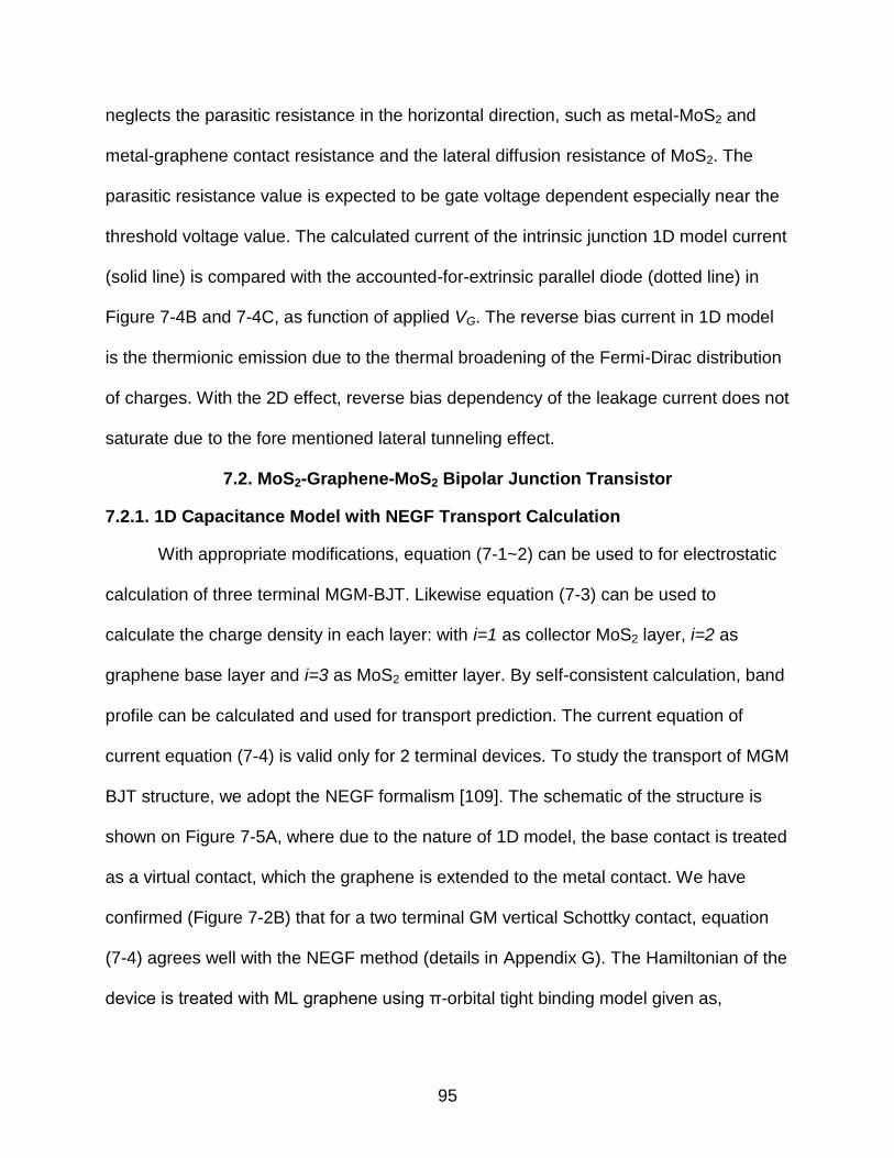
95
neglects the parasitic resistance in the horizontal direction, such as metal-MoS2 and
metal-graphene contact resistance and the lateral diffusion resistance of MoS2. The
parasitic resistance value is expected to be gate voltage dependent especially near the
threshold voltage value. The calculated current of the intrinsic junction 1D model current
(solid line) is compared with the accounted-for-extrinsic parallel diode (dotted line) in
Figure 7-4B and 7-4C, as function of applied VG. The reverse bias current in 1D model
is the thermionic emission due to the thermal broadening of the Fermi-Dirac distribution
of charges. With the 2D effect, reverse bias dependency of the leakage current does not
saturate due to the fore mentioned lateral tunneling effect.
7.2. MoS2-Graphene-MoS2 Bipolar Junction Transistor
7.2.1. 1D Capacitance Model with NEGF Transport Calculation
With appropriate modifications, equation (7-1~2) can be used to for electrostatic
calculation of three terminal MGM-BJT. Likewise equation (7-3) can be used to
calculate the charge density in each layer: with i=1 as collector MoS2 layer, i=2 as
graphene base layer and i=3 as MoS2 emitter layer. By self-consistent calculation, band
profile can be calculated and used for transport prediction. The current equation of
current equation (7-4) is valid only for 2 terminal devices. To study the transport of MGM
BJT structure, we adopt the NEGF formalism [109]. The schematic of the structure is
shown on Figure 7-5A, where due to the nature of 1D model, the base contact is treated
as a virtual contact, which the graphene is extended to the metal contact. We have
confirmed (Figure 7-2B) that for a two terminal GM vertical Schottky contact, equation
(7-4) agrees well with the NEGF method (details in Appendix G). The Hamiltonian of the
device is treated with ML graphene using π-orbital tight binding model given as,

96
0 0
0 0
2 cos
2 cos
x
x
iK
Dirac y
iK
y Dirac
E t t e KH K
t t e K E
, (7-7)
where 3 / 2y yK k a , 3 / 2x xK k a , intra-layer nearest-neighbor (NN) hopping
parameter, t0=2.7 eV and NN C to C atomic distance of a=1.42 Å. In the NEGF
formalism, electron transport across the layered device at given energy E is,
,
1, ,m n n m
K
T E trace E G E K E G E KA
, (7-8)
m,n is emitter (E), base (B) and collector (C) and
1
, E C BG E K EI H K E E
is the retarded greens function. A is the
total area of the Brillouin zone used for the numerical calculation. The two MoS2 layers,
emitter and collector, are dealt as phenomenological contacts to the graphene base and
expressed in the NEGF formalism as energy dependent self-energy ΣE and ΣC.
2E,C ,
1 0
0 12E C MoS
iD
The parameter γE,C in the definition of the self-energy (ΣE,C) is related to the inter-
layer transport coupling between graphene-MoS2 layers, same as N of current for GM
diode. Self-energy (ΣB) describes the phenomenological extension of graphene base
and the contact, and is expressed as,
1 0
0 12B B Gra
iD
.
The broadening matrix is
m m mi .

97
And lastly, the current density between the two nodes is calculated using
transmission from equation (7-8) as,
2
, ,
2m n m n m n
qI T E f E f E dE
h
.
The
1
1 exp mm
B
Ef E
k T
is the Fermi-Dirac distribution function at
temperature T. The chemical potential are, , , E E C C B BqV qV qV . The
applied voltage at each port, emitter, collector and base (VE, VC, VB, respectively) alters
the H(K) in equation (7-7) and thus varies the current. The current density at each node
is summation of each current density elements defined as,
, , E CE BE C CE CB B BE CBI I I I I I I I I .
As implied in the derivation, the properties of the contact self energy defines the
characteristic of the MGM BJT, thus careful engineering of γE,C and γB is required.
7.2.2. Results of the MGM BJT
As fore-mentioned the structure under study resembles that of the metal base
transistor (MBT) [108]. The short interlayer transit time is essential for high
performance, where the parameter ,E C is responsible in this model. Another to note is
that due to the high Fermi-velocity of graphene (VF=3×10⁶ m/s) [110], the excessive
base current will be the major drawback. To achieve large current gain (β=IC/IB),
suppressing the base current is critical. As the main purpose of this study is to illustrate
the operation mechanism of the device, we will examine the device behavior as a
function of , /E C B . Assuming the lateral extension of the graphene base is ~1 µm, and
in that the Fermi-velocity of graphene is 3×10⁶ m/s, the intrinsic delay time is in the

98
order of 0.33 psec. The value 5 2 28.0 10B eV nm results in the intrinsic delay time in
the similar order, and thus will be used through the investigation. The corresponding
scattering potential matrix element value is listed in Table 7-1. Figure 7-5B shows the
current density component (ICE,ICB,IBE) plot as function of VCB with MGM BJT in common
base configuration at VEB=-0.4 V, and 8 2 2
, 8.0 10E C eV nm . The value of ,E C is in the
similar range as have been extracted N earlier in GM junction section of the study. The
corresponding IC plot is in Figure 7-5D where, as VCB increase the two current plots with
varying VEB cross and at VCB>0, with larger (more negative) VEB, the current is smaller.
This is not the typical case for BJT with β >> 1. The reason for this can be found in
Figure 7-5B, where the IBE is larger than ICE. In this case, we cannot expect gain
(current gain or transconductance gain) from this device. As opposed to this case, with
increased graphene-MoS2 interlayer transport parameter to 4 2 2
, 1.6 10E C eV nm
(Figure 7-5C), we can find that the ICE exceeds IBE and as result, Figure 7-5E shows IC
larger with larger VEB in all VCB range as in a typical BJT. Figure 7-5F compares the IC
and IB of the two ,E C results. While IB is orders larger than IC for 8 2 2
, 8.0 10E C eV nm ,
current gain can be observed for 4 2 2
, 1.6 10E C eV nm case. Figure 6 A is plot of β,
intrinsic delay (τint) and graphene intralayer transport time (τB) as function of , /E C B .
The β show linear increase as , /E C B increase while τint show exponential decrease.
The τint was calculated as the below equation.
intB B
C CE CB
Q Q
I I I
(7-10)
Likewise, the

99
B BB
B CB BE
Q Q
I I I
.
The B is smaller than int at lower , /E C B , however, at , / 0.1E C B , become
similar, and at this point the 1 and further increase of , /E C B results in faster int
and larger . Figure 7-6B is to identify the effect of , /E C B on the current components.
The bias condition is VCB=0.2V which can be inferred from Figure 7-5E that is past the
saturation point, and VEB=-0.2 V. Both ICB and IBE are directly related to ,E C and B ,
thus show similar trend but shifted, while ICE show monotonic increase.
Although this study is focused on the GM junction and has utilized graphene as a
base of a MGM BJT, other combination is possible. Here, the effect of introducing a
bandgap material in the base is investigated. Figure 7-7 shows the numerical
calculation results on BJT structures with artificial 2D material in the base. The adopted
2D material has DOS as a graphene but with a bandgap of 0.1 eV and 0.8 eV. Figure 7-
7A, depicts the energy dependent DOS of the graphene and graphene with bandgap.
Figure 7 B shows the band profile at VCB=0 V and VEB=-0.4 V. From this figure we can
expect the dramatic reduction of ICB and IBE with larger bandgap, which translates to
large decrease in IB. Figure 7-7C~E compares the transmission of the two cases as
function of energy between, C-E, B-E and C-B respectively. The large bandgap clearly
blocks the transmission, especially Figure 7-7E show large reduction for C-B
transmission. Thus, large decrease in both the IC and IB is expected and is confirm by
Figure 7-7 F. Although the overall current level has been reduced, the introduction of
bandgap benefits the current gain as plotted in Figure 7-7G.

100
Summary
Graphene-MoS2 junction was studied using numerical methods. Comparing with
measurement and 2D Poission calculation, we have found the cause of linear reverse I-
V characteristic in the lateral tunneling junction. Also, interlayer transport parameter has
been extracted to predict the performance of 3 terminal MGM BJT. The major drawback
of this MBT-like device is the large base current. Careful engineering of ,E C and B
ratio, which is physically related to the interlayer transport property is required to
achieve certain current gain. We also find that the base material with bandgap results in
reduction of overall current density, however is preferred in achieving large current gain.

101
Table 7-1. Scattering potential matrix element value
γE,C/γB § 1.0×10
-3 1.0×10
-2 1.0×10
-1 2.0×10
-1 1 2 3
γE,C [eV2nm
2] 8.0×10
-8 8.0×10
-7 8.0×10
-6 1.6×10
-5 8.0×10
-5 1.6×10
-4 2.4×10
-4
MB02[eV
2nm
2] 0.0825 0.825 8.25 16.5 82.5 165 247
§ B is set to a constant value of 5 2 28.0 10 eV nm
Figure 7-1. Simulated structure of graphene-MoS2 junction. A) 2 Dimensional (2D) and B) 1 dimensional (1D) schematic of the graphene-MoS2 junction. C) 1D capacitance model.

102
Figure 7-2. MoS2-Graphene junction properties. A) Measured I-V plot of MoS2-Graphene diode with varying gate bias (VG). B) Extracted conductance from measured I-V compared with numerical results. C) Graphene-MoS2 interlayer electron transport time (τ). D) Conduction band energy of bottom MoS2 (EC,MoS2) and Dirac point of top graphene (EDirac) as function of VG and E) difference between the two value.
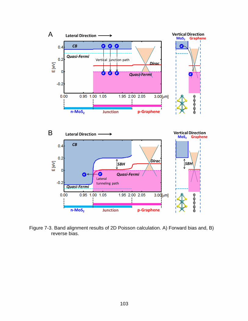
103
Figure 7-3. Band alignment results of 2D Poisson calculation. A) Forward bias and, B) reverse bias.

104
Figure 7-4. Isolated diode model and its results. A) Isolated diode model to describe the leakage current at reverse bias. B) I-V curve in logarithm scale. C) I-V curve in linear scale. The solid line represents result from 1D model. Dashed line represents results from isolated diode model.
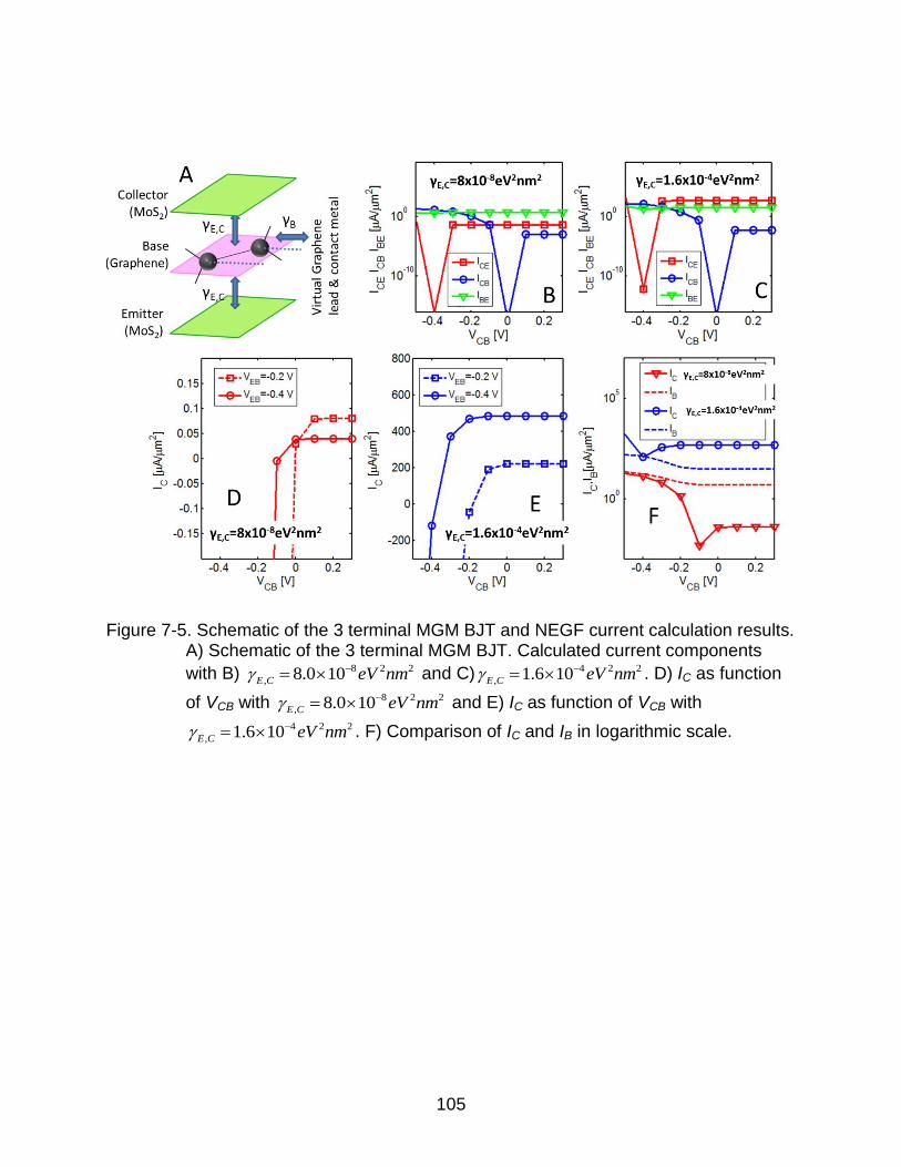
105
Figure 7-5. Schematic of the 3 terminal MGM BJT and NEGF current calculation results. A) Schematic of the 3 terminal MGM BJT. Calculated current components
with B) 8 2 2
, 8.0 10E C eV nm and C) 4 2 2
, 1.6 10E C eV nm . D) IC as function
of VCB with 8 2 2
, 8.0 10E C eV nm and E) IC as function of VCB with
4 2 2
, 1.6 10E C eV nm . F) Comparison of IC and IB in logarithmic scale.

106
Figure 7-6. Current gain and intrinsic delay of the MGM-BJT. A) Extracted current gain (β), intrinisic delay (τint) and graphene intralayer transport time (τB) as function
of , /E C B . B) Extracted current components as function of , /E C B .

107
Figure 7-7. Predicted performance of MGM-BJT with bandgap base. A) Artificial badgap induced graphene DOS with bandgap of 0.1eV and 0.8 eV. B) Band diagram of the MGM BJT. (C~E) Transmission as function of energy between, C-E, B-E and C-B respectively. F) IC and IB as function of VCB and G) corresponding current gain (β).

108
CHAPTER 8 CONCLUSION
The first demonstration of graphene [7] unveiled series of 2D layered material for
the future nano-devices. Such material includes h-BN, topological insulators, and
transition metal dichalcogenides (TMDs). Graphene has been of a great interest due to
its fascinating properties such as mobility in the order of 105 cm2/V∙s, thermal
conductivity up to 3000 W/K∙m [48,49]. However, due to the absence of band gap, the
graphene-based FETs have high off-current and thus is not suitable for current logic
applications. In this work, we have proposed few ways to induce the bandgap in the
graphene by functionalization. Also we have looked into TMDs, which are 2D materials
that naturally bear bandgap. One purpose of this work is to understand the material
properties, such as band-structure which convey the essential character of the material,
doping feature, and electrostatic screening behaviors. Another is to understand
operation mechanism and project the performance of devices that use these 2D
materials.
In the first topic, which is Chapter 2 of this dissertation, we have investigated
electronic properties of A-Cx(BN)ys through DFT calculation. An earlier study has shown
that the domains of graphene can be grown in the 2D h-BN sheet [29]. Motivated from
this, we proposed a structure, A-Cx(BN)y, which is analogous to the AGNRs. The
confinement is provided from the h-BN to induce bandgap in the graphene system. The
bandgap properties of A-Cx(BN)y resembles that of the AGNR. However, considerably
bandgap opening for A-Cx(BN)ys with width index of 3p+2 is observed. Also the relation
of the width to the bandgap in A-Cx(BN)ys, follows the hierarchy as E3p+2<E3p+1<E3p, as
opposed to AGNRs’ hierarchy of E3p+2<E3p<E3p+1. We find the cause of this as the

109
perturbation from the large ionic potential difference between B and N. A TB model of
the system was constructed as a simple and effective method to confirm out theory and
predict the electronic properties.
As an extension of the first work on A-Cx(BN)y, we have looked into chemical
modified graphene, i.e., graphane, to induce confinement on the graphene system. The
band structure of partially hydrogenated graphene, graphene nanoroad and graphene
nanomesh were studied and showed that a considerable bandgap can be achieved in a
continuous 2D layer. We also found through top-barrier ballistic MOSFET model that the
highly non-isotropic 2D E-k of graphene nanoroad is preferred in achieving higher
device performance.
Moving the focus from generating bandgap in graphene to 2D material with
bandgap, we look into TMDs. In Chapter 4 of this dissertation, we have studied the
potassium (K) doping features in MoS2 and WSe2, and compared it with the graphene,
through DFT calculations. K has a small electron affinity and thus is acts as a strong
electron donor. While the K doping in graphene has been reported to be unstable [58],
our study shows that K-MoS2 and K-WSe2 bonding to be stronger, thus more reliable.
By adopting mechanical transfer process [64], various types of 2D material can
be stacked, which leads to study of stacked heterojunctions. As prior to understanding
the junction physics, we studied the electrostatic screening behavior of multilayer TMDs
(we have work on MoS2, however, same method can be applied to other TMDs)
following the method of a graphene stack [97]. By using numerical methods, we found
the electrostatic screening to be highly dependent on applied gate voltage and
temperature. The major difference between multi-layer graphene is that, the graphene

110
has saturating screening length which is due to its semi-metallic feature. On the other
hand, MoS2, due to the sufficient large bandgap of 1.8 eV, the screening length can
extend to infinity. We also derive analytical expression for the Debye length which
suggests that the lower limit of the screening length to be around half of the interlayer
distance of MoS2 layers.
As for the last topic, we have investigated the properties of graphene-MoS2
vertical junction. As graphene is semi-metallic material, this junction resembles the
metal-semiconductor junction. However, due to their 2D nature and also geometry of
the junction, which extends to form a contact, leads to lateral tunneling junction at the
reverse bias. This result in a linear I-V characteristic, that cannot be found in the
traditional MS junction. Also, interlayer transport parameter has been extracted to
predict the performance of the 3 terminal MGM BJT. The major drawback of this MBT-
like device is the large base current. Careful engineering of ,E C and B ratio, which is
physically related to the interlayer transport property is required to achieve certain
current gain. We also find that the base material with bandgap is preferred for large
current gain.
These works can be extended to explore other 2D materials. One of such
material may be black phosphorus. This has recently gained interest in that it has highly
non-isotropic direct bandgap 2D band structure [114,115]. The peculiar crystalline
structure enables the band be tailored with applied strain which the origin is yet unclear.
In depth study via DFT is needed to understand the physics. Also the anisotropic band
structure will lead to interesting study of the transport properties.

111
APPENDIX A BANDGAP CALCULATION OF AGNR AND AGNR WITH EDGE PERTURBED BY THE
IONIC POTENTIAL
A.1. Derivation of Bandgap for AGNRs
AGNRs are semiconductors with bandgap which decrease as the width increase
and in the larger width limit will function as graphene. However, the variation of the
bandgap follows a distinctive behavior as function of the width and can be categorized
into three groups depending on the width, e.g., n=3p, 3p+1 and 3p+2. Here, we will
derive the bandgap characteristic of each family member and carry on the derivation of
the perturbed AGNR system in appendix A.2, where the perturbation is due to the
neighboring B and N atoms that are dealt in chapter 2 of the text.
Figure A-1. Graphene nanoribbon schematic. A) Schematic of AGNR with width(n) of Na=9 in this case. B) Topologically equivalent structure of Na-AGNR C) Topologically equivalent structure of Na-AGNR in the case of k=0. All the sublattices are linked with tight binding parameter t0.
The AGNR, as depicted in Figure A-1 A can be viewed topologically same as
Figure A-1 B which can be further simplified, in the condition that k=0, to Figure A-1 C
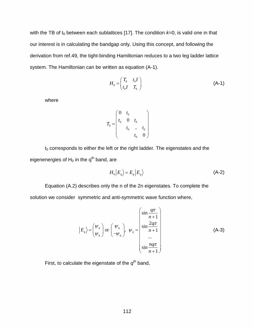
112
with the TB of t0 between each sublattices [17]. The condition k=0, is valid one in that
our interest is in calculating the bandgap only. Using this concept, and following the
derivation from ref.49, the tight-binding Hamiltonian reduces to a two leg ladder lattice
system. The Hamiltonian can be written as equation (A-1).
0 0
0
0 0
T t IH
t I T
(A-1)
where
0
0 0
0
0 0
0
0
0
..
0
t
t tT
t t
t
t0 corresponds to either the left or the right ladder. The eigenstates and the
eigenenergies of H0 in the qth band, are
0 q q qH E E E (A-2)
Equation (A.2) describes only the n of the 2n eigenstates. To complete the
solution we consider symmetric and anti-symmetric wave function where,
sin1
2sin
or , 1
...
sin1
q q
q q
q q
q
n
q
E n
nq
n
(A-3)
First, to calculate the eigenstate of the qth band,

113
0
0 0
0 0 0
0 0
0
0 ... ... ...
0 ( 1) ( 1)sin sin sin 2sin cos
.. 1 1 1 1 1
... ... ...0
q
t
t t iq i q i q iq qT t t
t t n n n n n
t
which results in,
0 02 cos1
q q
qT t
n
. (A-3)
And to solve for the Hamitonian,
0 0 0 0
0
0 0 0 0
or q q
q
q q
T t I T t IH E
t I T t I T
which leads to ,
0 0 0 0 02 cos or 2 cos1 1
q q
q
q q
q qH E t t t t
n n
.
Thus, as for the general solution of the eigenenergies of the qth subband is,
0 1 2cos1
q
qE t
n
and
0 1 2cos1
q
qE t
n
, (A-4)
where, 1,2,3...q n .
We can further derive the solution of the eigenenergies into the 3 categories of
the AGNR family.
A.1.1. Case 1. n=3p
0 1 2cos3 1
q
qE t
p
,
with 1,2,3...3q p . For this to have minimum value, 3 1 3
q
p
. Thus, at q=p,
,min 0 1 2cos3 1
q
pE t
p

114
So, the bandgap of the AGNR with width of n=3p is,
0
, 3 02 1 2cos3 1
g n p
pE t
p
(A-5)
A.1.2. Case 1. n=3p+1
Similarly,
0 1 2cos3 2
q
qE t
p
,
with 1,2,3...(3 1)q p and for this to have minimum value, 2
3 2 3
q
p
. Thus, at
q=p+1, ,min 0 0
(2 1) ( 1)1 2cos 1 2cos
3 2 3 2q
p pE t t
p p
,
0
, 3 1 0
( 1)2 1 2cos
3 2g n p
pE t
p
(A-6)
A.1.2. Case 3. n=3p+2
0 1 2cos3 3
q
qE t
p
, with 1,2,3...(3 2)q p and for this to have minimum
value, 3 3 3
q
p p
and thus, at q=p+1, ,min 0qE , , 3 2 0g n pE

115
A.2. Bandgap AGNR Perturbed by the Ionic Potential of B and N at the AGNR Edge
Figure A-2. Schematic of AGNR and perturbation modeling. A) Schematic of AGNR perturbed at the four edge C atoms by the neighboring B and N of the AGNR of the for A-Cx(BN)y system in chapter 2. B) Simplified ladder representation. C) Case for the even and odd AGNR width.
To calculate the bandgap of the AGNR confined by BNNR (A-Cx(BN)y) through
perturbation calculation, we need to account for the perturbed Hamiltonian.
1
1 0H H H
The 0H is the Hamiltonian of the AGNR itself, which has been derived in
appendix A.1, and 1H is the first order perturbation. We set the perturbation
Hamiltonian as,
1
1
2
0
0
TH
T
.

116
The off diagonal terms are zero matrix in that we assume nothing has affected
the C-C interaction of the original AGNRs (we simplify the problem to just perturbation in
the ionic onsite energy of the C atoms at the edge as represented in Figure A-2 A and
B).
1 2 ,
a b
a b
E E
T T
E E
n=odd
1 2 ,
a b
b a
E E
T T
E E
n=even
The 1st order perturbed eigenenergies can be written as,
1
1 2
0
0
2
q
q qq q q
q
q qq q
T
E H E TE
E E
(A-7)
First, solving the denominator,
2
1 1
1 cossin
1 2
n n
q q
m m
mmq
n
, where
2
1
q
n
Thus,
1
1 1 1 ( 1)cos 1 sin cos
2 2 sin( / 2) 2 2
n
q q
m
n nn m n

117
1 1 2 ( 1) 21 sin cos
1 22 1 2 2 1sin( )2 1
1 11 sin cos , since q is intger
2 1sin( )1
1( 1)
2
q q
q n n qn
q n n
n
nqn q
q n
n
n
Moving on to the nominator,
1
1 1 2
2
0
0
q
q q q q q q
q
TE H E T T
T
.
For both even and odd cases,
1 2
a b
a b
E E E
T T
E E E
, a bE E E
Thus,
1 2 2 2
sin1
0
sin sin..1 1
0
sin1
q q q
qE
n
q nqT T E
n n
nqE
n
A.2.1. Case 1. n=3p
With q=p,
2
1 2 2 2 3sin sin
3 1 3 1q q
p pT T E
p p
,
and thus,

118
22 2
3 sin sin1 3( 1) 3( 1)
a an p
E E n nE
n n n
Resulting bandgap calculation for n=3p is,
20 2 2
, 3 , 3 2 sin sin1 3( 1) 3( 1)
a bg n p g n p
E E n nE E
n n n
(A-8)
A.2.2. Case 1. n=3p+1
With q=p+1, as in the AGNR case the anti-symetric solution results in the
minimum value of the eigenergy, and thus solving for that results in.
The resulting bandgap calculation for n=3p is,
0 2 2
, 3 1 , 3 1
2 ( 2)2 sin sin
1 3( 1) 3( 1)
a bg n p g n p
E E n n nE E
n n n
1
1 1 2 2 2
2
0 2 ( 2)sin sin
3( 1) 3( 1)0
q
q q q q q q
q
T n n nE H E T T E
n nT
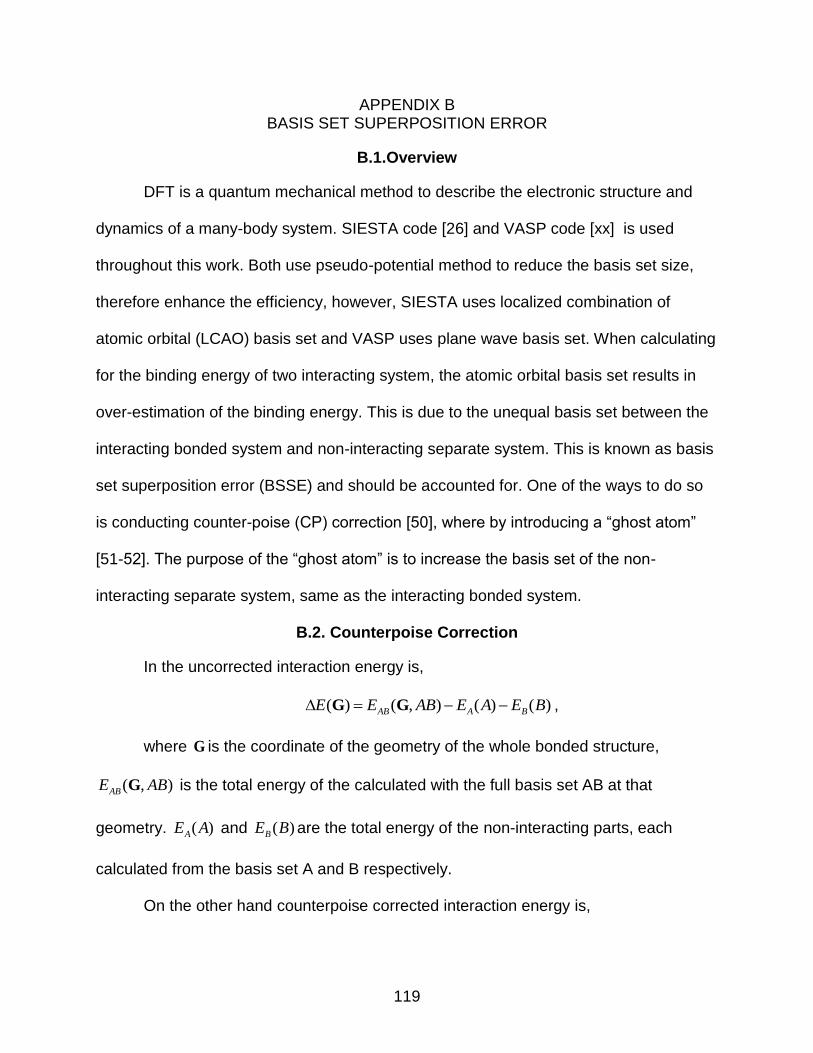
119
APPENDIX B BASIS SET SUPERPOSITION ERROR
B.1.Overview
DFT is a quantum mechanical method to describe the electronic structure and
dynamics of a many-body system. SIESTA code [26] and VASP code [xx] is used
throughout this work. Both use pseudo-potential method to reduce the basis set size,
therefore enhance the efficiency, however, SIESTA uses localized combination of
atomic orbital (LCAO) basis set and VASP uses plane wave basis set. When calculating
for the binding energy of two interacting system, the atomic orbital basis set results in
over-estimation of the binding energy. This is due to the unequal basis set between the
interacting bonded system and non-interacting separate system. This is known as basis
set superposition error (BSSE) and should be accounted for. One of the ways to do so
is conducting counter-poise (CP) correction [50], where by introducing a “ghost atom”
[51-52]. The purpose of the “ghost atom” is to increase the basis set of the non-
interacting separate system, same as the interacting bonded system.
B.2. Counterpoise Correction
In the uncorrected interaction energy is,
( ) ( , ) ( ) ( )AB A BE E AB E A E B G G ,
where G is the coordinate of the geometry of the whole bonded structure,
( , )ABE ABG is the total energy of the calculated with the full basis set AB at that
geometry. ( )AE A and ( )BE B are the total energy of the non-interacting parts, each
calculated from the basis set A and B respectively.
On the other hand counterpoise corrected interaction energy is,

120
( ) ( , ) ( , ) ( , )CP
AB A AE E AB E AB E AB G G G G ,
where ( , )AE ABG and ( , )BE ABG is the total energies of part A and B,
calculated within the basis set of AB at geometry G , respectively. This can be
understood as increasing the basis set size of each element A and B to the whole AB
structure. Thus BSSE can be calculated as, ( ) ( )CPBSSE E E G G .
B.3. Calculating the C-H Binding Energy of A-HNRs Using Counterpoise Correction
By using the CP corrected method we can extract the H or the F binding energy
to the graphene system. Figure A-3 A shows the atomic structure of the A-HNR. From
Figure A-3 B, the side view of the unitcell , we can see that the H atoms are puliing the
binding C atoms out of the graphene plane which indicates that the basis set of the A-
HNRs will differ from that of just the H atoms and the graphene. To account for the
arising BSSE, we need to set the basis set equal by introducing the “ghost atoms”. First,
by the DFT calculation, we calculate the molecular dynamically relaxed geometry (or the
atomic coordinates) and the total energy ( ( , )A HNRE A HNR G ) of the A-HNR structure.
From the obtained atomic coordinates, we run the second un-relaxed DFT calculation
with all the C atoms set to ghost atoms as in Figure A-3 D and obtain the total energy,
( , )HE A HNRG . Third conduct un-relaxed DFT calculation of the graphene with the H
atoms as ghost atoms as in Figure A-3 (e) and get ( , )A NRE A HNR G .
The resulting binding energy can be calculated as,
( , ) ( , ) ( , )CP A HNR H A NR
H
E A HNR E A HNR E A HNRE
n
G G G,

121
where nH is the number of H atoms in the unitcell of the A-HNR and CPE is the
binding energy of a H atom.
Figure B-1.BSSE calculation method. A) Atomic structure of unitcell of A-HNR, top view. B) Side view of the unitcell of A-HNR. Notice that C atoms with H bonded is pulled out of the graphene plane indicating that the atomic basis has been modified from that of graphene. C) Schematic of A-HNR. D) Schematic of H atoms with the basis set extended to the same basis set of the A-HNRs, where the dotted atoms represent the ghost atoms of the graphene. E) Schematic of graphene with the basis set extended to the same basis set of the A-HNRs, where the dotted atoms represent the ghost atoms of the H.

122
APPENDIX C G0W0 CALCULATION APPROACH
In the following GW quasi-particle (QP) calculation, non-self-consistent G0W0
was used to reduce the computational cost [79]. Same atomistic relaxed structure was
used as in the main text. HSE exchange-correlation functional was used to obtain wave
functions for the GW calculation. Although this step is not essential, this method has
been suggested to improve agreement with experiments [90]. The Brillouin zone
sampled with a 6 × 6 × 1 k-point mesh. The band-structure was Wannier interpolated
using the WANNIER90 program [91]. From the Figure CA, ~0.65 eV shift of CBM as
regard to the valence band can be observed. In Figure CB, splitting the valence bands
due to spin orbital coupling is shown.
Figure C-1. Bilayer WSe2 HSE-DFT and G0W0 calculation. A) Comparison of Wannier interpolated HSE-DFT and G0W0 calculation. SOC is not considered and no strain is applied. B) Comparison of spin orbital coupling (SOC) effect in HSE-DFT calculation. Band splitting in the K point of the valence band can be observed.

123
APPENDIX D VASP INPUT SCRIPT FOR GGA, HSE AND G0W0 SIMULATION
D.1. GGA
In Cpater 5, structural relaxation was performed using GGA XC functional. In the
VASP calculation, for fast and accurate results, first, (1) ISIF was set as 7 in the input
script (INCAR). This maintains the overall shape of the geometry from the initial guess
during the relaxation process but modified the cell volume. Once this calculation is
converged, using the updated geometry (saved as CONTCAR, update the POSCAR to
CONTCAR), another relaxation calculation was performed, with (2) ISIF=2. This
procedure relaxes the ions without changing the cell shape or the volume. The resulting
structure will be relatively precise, however, to further improve accuracy, these two
steps can be iterated. With the resulting relaxed structure, (3) self-consistent calculation
is followed with higher k-mesh grid. Then last step is the (4) bandline calculation. Below
is the INCAR script for the process.
Table D-1. GGA step 1 and 2
INCAR file Comments KPOINT file System = BL_WSe2 PREC = NORMAL SYMPREC = 1E-8 ENCUT = 400 ISTART = 0 ICHARG = 2 NELMIN = 6 EDIFF = 1E-5 NSW = 100 IBRION = 2 ADDGRID = .TRUE. ISIF = 7 ISMEAR = 0 SIGMA = 0.05 GGA = PE LVDW = .TRUE. VDW_C6 = 12.64 48.894 VDW_R0 = 1.771 1.8413
ISTART=0 for step (1), 1 for step (2). For iterating of these steps use 1. ICHARG=2 for step (1), 1 for step (2). For iterating of these steps use 1. ISIF=7 for step (1) and 2 for step (2) Last three lines are to include the effects of the vdW force vias DFT-D2 method
k-points 0 Gamma 9 9 1 0 0 0

124
Table D-2. GGA step 3
INCAR file Comments KPOINT file PREC = ACCURATE LSORBIT = .TRUE. LORBIT = 11 SYMPREC = 1E-8 ENCUT = 400 ISTART = 1 ICHARG = 1 NELMIN = 6 EDIFF = 1E-7 NSW = 0 ADDGRID = .TRUE. ISMEAR = 0 SIGMA = 0.05 GGA = PE LVDW = .TRUE. VDW_C6 = 12.64 48.894 VDW_R0 = 1.771 1.8413
LSORBIT=.TRUE. switches on spin-orbit coupling LORBIT = 11 : quick method for the determination of the spd- and site projected wave function character
Increase the k mesh points for improved accuracy KPOINTS k-points 0 Gamma 15 15 1 0 0 0
Table D-3. GGA step 4
INCAR file Comments KPOINT file PREC = ACCURATE LSORBIT = .TRUE. LORBIT = 11 SYMPREC = 1E-8 ENCUT = 400 ISTART = 1 ICHARG = 11 NSW = 0 IBRION = -1 LWAVE = .FALSE. LCHARG=.FALSE. ADDGRID = .TRUE. ISMEAR = 0 SIGMA = 0.05 GGA = PE LVDW = .TRUE. VDW_C6 = 12.64 48.894 VDW_R0 = 1.771 1.8413
ICHARG=11: To obtain the eigenvalues (for band structure plots) or the DOS for a given charge density read from CHGCAR.
k-points 50 Line-mode rec 0.66666667 0.33333333 0.00000000 ! K 0.00000000 0.00000000 0.00000000 ! Gamma 0.00000000 0.00000000 0.00000000 ! Gamma 0.50000000 0.00000000 0.00000000 ! M 0.50000000 0.00000000 0.00000000 ! M 0.66666667 0.33333333 0.00000000 ! K
D.2. HSE
VASP input script (INCAR and KPOINTS) are shown below. The script contains
self-consistent calculation, which require relaxed atomistic structure, and the band
calculation. Note that the INCAR file is basically same. However, for band calculation,
the k points in KPOINTS file must be specified with weighting of 0. Also to generate
orbital resolved bands, flag “LSORBIT = .TRUE.” must be included in INCAR. This
results in output file of PROCAR that contains the information.
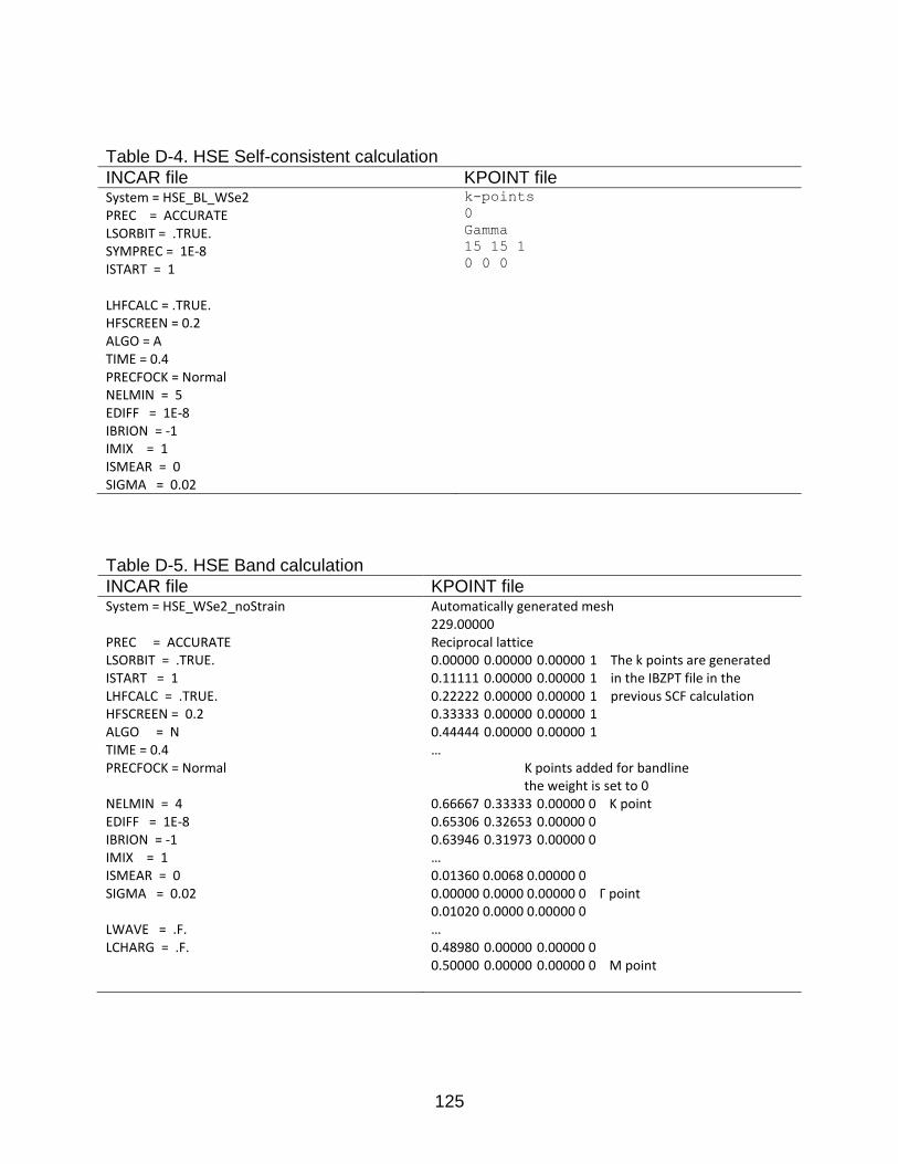
125
Table D-4. HSE Self-consistent calculation
INCAR file KPOINT file System = HSE_BL_WSe2 PREC = ACCURATE LSORBIT = .TRUE. SYMPREC = 1E-8 ISTART = 1 LHFCALC = .TRUE. HFSCREEN = 0.2 ALGO = A TIME = 0.4 PRECFOCK = Normal NELMIN = 5 EDIFF = 1E-8 IBRION = -1 IMIX = 1 ISMEAR = 0 SIGMA = 0.02
k-points
0
Gamma
15 15 1
0 0 0
Table D-5. HSE Band calculation
INCAR file KPOINT file System = HSE_WSe2_noStrain PREC = ACCURATE LSORBIT = .TRUE. ISTART = 1 LHFCALC = .TRUE. HFSCREEN = 0.2 ALGO = N TIME = 0.4 PRECFOCK = Normal NELMIN = 4 EDIFF = 1E-8 IBRION = -1 IMIX = 1 ISMEAR = 0 SIGMA = 0.02 LWAVE = .F. LCHARG = .F.
Automatically generated mesh 229.00000 Reciprocal lattice 0.00000 0.00000 0.00000 1 The k points are generated 0.11111 0.00000 0.00000 1 in the IBZPT file in the 0.22222 0.00000 0.00000 1 previous SCF calculation 0.33333 0.00000 0.00000 1 0.44444 0.00000 0.00000 1 … K points added for bandline the weight is set to 0 0.66667 0.33333 0.00000 0 K point 0.65306 0.32653 0.00000 0 0.63946 0.31973 0.00000 0 … 0.01360 0.0068 0.00000 0 0.00000 0.0000 0.00000 0 Γ point 0.01020 0.0000 0.00000 0 … 0.48980 0.00000 0.00000 0 0.50000 0.00000 0.00000 0 M point

126
D.3. G0W0
The G0W0 calculation is performed over HSE wave functions. Thus require
WAVECAR file obtained from HSE self-consistent calculation. For G0W0, the input of the
KPOINTS file is the Monkhorst-Pack (MH) scheme. The bandline calculation as in HSE
or other XC is not adaptable for GW approach. The band is Wannier interpolated from
the k mesh using WANNIER90 [91]. For honeycomb lattice structure, to sample all high
symmetry points (Κ,Μ,Γ) multiple of 6 is required in the MH k mesh. Here for calculation
cost purpose we use 6x6x1.
Table D-6. HSE Band calculation INCAR file.
Step 1 Step 2 Step 3 System = WSe2 PREC = ACCURATE ISTART = 1 ICHARG = 1 # charge: 1-file EDIFF = 1E-5 IBRION = -1 ISMEAR = 0 SIGMA = 0.02 LHFCALC = .T. HFSCREEN= 0.2 ALGO = A TIME = 0.4 LWANNIER90_RUN=.T. LWRITE_MMN_AMN=.T.
System = WSe2 PREC = ACCURATE ISTART = 1 ICHARG = 1 EDIFF = 1E-5 IBRION = -1 ISMEAR = 0 SIGMA = 0.02 LHFCALC = .T. HFSCREEN= 0.2 TIME = 0.4 ALGO = Exact NBANDS = 300 LOPTICS = .T. NEDOS = 2000
System = WSe2_BL PREC = ACCURATE ISTART = 1 ICHARG = 1 IBRION = -1 ISMEAR = 0 SIGMA = 0.02 LHFCALC = .T. HFSCREEN= 0.2 TIME = 0.4 NBANDS = 304 ALGO = GW0 LSPECTRAL = .T. NOMEGA = 50 LWANNIER90_RUN=.T. LWRITE_MMN_AMN=.T.

127
APPENDIX E ANALYTICAL DERIVATION OF DEBYE LENGTH
In a 1D system, with the varying space charge density of ( )x ,the potential V x
can be calculated by solving the Poisson’s equation,
2
2
2
0r
d V x xV x
dx
.
In the n-type semiconductor this rewritten as,
2
0 2r
d V dnq dV
dx dV (E-1),
where n is the electron density and q is the elementary charge. Here, the
gradient of n to the V is the DOS. For the n-type semiconductors, the DOS within a
small potential range near the EC can be approximated as,
1 1eff
dn nD
q dV q V ,
which results in effn qD V . Thus equation (E-1) can be simplified to,
22
0 20r eff
d Vq D V
dx ,
and this second-order differential equation can be solved by comparing with,
0 expD
xV x V
which results in the Debye length ( D ) of,
0
2
rD
effq D
. (E-2)
If we apply Boltzmann's carrier distribution to approximate the charge density as,
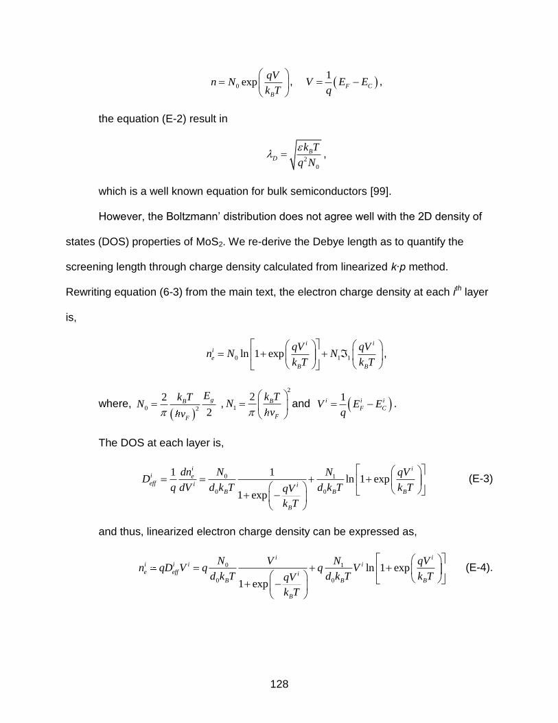
128
0 expB
qVn N
k T
,
1F CV E E
q ,
the equation (E-2) result in
2
0
BD
k T
q N
,
which is a well known equation for bulk semiconductors [99].
However, the Boltzmann’ distribution does not agree well with the 2D density of
states (DOS) properties of MoS2. We re-derive the Debye length as to quantify the
screening length through charge density calculated from linearized k∙p method.
Rewriting equation (6-3) from the main text, the electron charge density at each ith layer
is,
0 1 1ln 1 expi i
i
e
B B
qV qVn N N
k T k T
,
where,
0 2
2
2
gB
F
Ek TN
v ,
2
1
2 B
F
k TN
v
and
1i i i
F CV E Eq
.
The DOS at each layer is,
0 1
0 0
1 1ln 1 exp
1 exp
i ii eeff i i
B B B
B
dn N N qVD
q dV d k T d k T k TqV
k T
(E-3)
and thus, linearized electron charge density can be expressed as,
0 1
0 0
ln 1 exp
1 exp
i ii i i i
e eff iB B B
B
N NV qVn qD V q q V
d k T d k T k TqV
k T
(E-4).

129
Through self consistent iteration with 1D capacitance model [equation (6-2) in the
main text] and equation (E-4), the potential iV and electron charge density ( i
en ) can be
found. Inserting i
effD to equation (E-2), Debye length can be found as,
0 0
0 0
2
0 2
1
1 exp
ln 1 exp
i
r B
Bi r BD i
B
qVd k T
k T d k T
q N qVq N
k T
. (E-5)

130
APPENDIX F EVALUATION OF 2D THOMAS-FERMI MODEL
Here we provide the derivation of the two dimensional (2D) Thomas-Fermi (TF)
model to evaluate the screening characteristics on multi-layer MoS2. The details can be
found in ref 101. Also, derivations for graphene multilayer can be found in ref 100. We
use parabolic conduction band 2
2 2 2 MoSE k m , located at the K points of the Brillouin
zone, with valley and spin degeneracy ( vN , sN ) of 2 and in-plane effective mass (2MoSm )
of 0.52m0. The kinetic energy (per unit area) of each layer of MoS2 can be expressed
as,
2
0TF TFE Q z A Q z , where
2
2
0
s v MoS
AN N m
.
In the continuum limit, the grand potential for this system is,
2 2
2 2
0
0 , 0 , 0 00 0
'' '
2 4
D D
TF TF TF TF TF
r MoS r MoS
ze Qdz e dzE Q z Q Q z Q z z z Q z
d d
.
(F-1)
is the chemical potential, D is the total thickness of the MoS2 layers. 0d is the
interlayer distance between the MoS2 layers with a value of 6Å as in the main text. The
screening properties are obtained by minimizing with respect to the charge density
TFQ z . This leads to a differential equation of,
2
2 20 0
0 0
2 2TF TF TF
dQ z Q z Q D
dz d d
, (F-2)
where, 2
2
0 , 0 04 r MoSe A . The corresponding boundary conditions are as
follows.
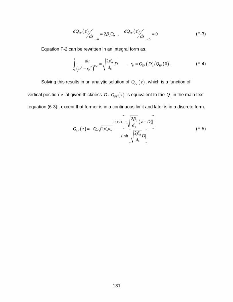
131
0 0
0
2 , 0 TF TF
z z D
dQ z dQ zQ
dz dz
(F-3)
Equation F-2 can be rewritten in an integral form as,
1
0
1/22 2
0
2
Dr D
duD
du r
, 0D TF TFr Q D Q . (F-4)
Solving this results in an analytic solution of FTQ z , which is a function of
vertical position z at given thickness D . FTQ z is equivalent to the iQ in the main text
[equation (6-3)], except that former is in a continuous limit and later is in a discrete form.
0
0
0 0 0
0
0
2cosh
22
sinh
TF
z Dd
Q z Q d
Dd
(F-5)

132
APPENDIX G INTERLAYER COUPLING FACTOR αC AND αN
In the main text, to calculate the interlayer current, classical approach is used.
This method utilizes the DOS of the graphene and MoS2 layers and an interlayer
transport parameter αC. The NEGF formalism can also be used for the same purpose.
To do so, interlayer transport parameter (we denote as αN) needs to be redefined to suit
the formalism. As in the main text Chapter 7.2.1, the Hamiltonian of the device is treated
with ML graphene using π-orbital tight binding model,
0 0
0 0
2 cos
2 cos
x
x
iK
Dirac y
iK
y Dirac
E t t e KH K
t t e K E
,
where 3 / 2y yK k a , 3 / 2x xK k a , intra-layer nearest-neighbor (NN) hopping
parameter, t0=2.7 eV and NN C to C atomic distance of a=1.42 Å. Transmission across
the layered device at given energy E is,
2MoS Gra
1, ,
K
T E trace E G E K E G E KA
,
2
1
, MoS GraG E K EI H K E E
is the retarded greens function. A is
the total area of the Brillouin zone used for the numerical calculation. The contact self-
energy needs to be defined in a way that the physical fitting parameter can be
introduced. The Table G-1 compares the classical method to the NEGF formalism for
convenience of understanding. The term 2C Gra MoSD E D E is physically equivalent to
the transmission function derive form the NEGF. As the MoS2 layer is treated as a
contact to the graphene channel (Hamiltonian matrix), interlayer transport parameter is

133
buried inside the self-energy (or the broadening matrix). Within the NEGF formalism, the
self-energy can be expressed in terms of DOS as below.
2 2 2
22 2MoS MoS MoSD D
Here, represents the device-reservoir (contact) coupling, unit in eV∙m. Thus,
the N in the main text is 2
, and connection to the classical parameter C is as,
2 2 2 2
22 2MoS MoS N MoS C MoSD D D .
2
CN
.
Table G-1. Classical and NEGF transport calculation comparison
Classical Approach NEGF approach
2 2
2 C Gra MoS Gra MoS
qI D E D E f E f E dE
h
2
2Gra MoS
qI T E f E f E dE
h
2
C Gra MoSD E D E 2
,
1
x y
MoS Gra
k k
T E trace E G E E G EA
GraD E ,
1 1
2x y
Gra
k k
trace G E E G EA
2
C MoSD E 2MoS E

134
APPENDIX H EXTRACTION OF INTERLAYER COUPLING FACTOR AND RELATION TO NEGF
A transport model for determining the interlayer current for tunneling transistor
adopting 2D semiconductors have been proposed [111]. The procedure was followed to
determine the fore-mentioned interlayer tunneling parameter αC and αN of this work. The
interlayer current between two 2D semiconductors (top and bottom represented as
subscript T and B, respectively) can be computed by the Landauer-Buttiker formula
[112],
,T B
v s TB T B
eI g g dE T E f E f E
h
k k
. (H-1)
The vg (
sg ) is the valley (spin degeneracy), ,T Bf is the Fermi-Dirac distribution
function and TBT is the interlayer transmission between the wave state with wave vectors
of Bk and
Tk . e is the elementary charge. Under assumption of weak interlayer
coupling, which has been consistent within this work, can be express in terms of DOS
(or the spectral function) and the scattering potential matrix element, TBM as,
TB T TB B TBT E A E M A E M .
The spectral function is,
, , ,2T B T B T BA E E E k
,
where , ,T B T BE k is the E-k relation of the top and bottom layer. Thus, returning to
equation (H-1) results in the interlayer current as [111],
2
,
,T B
v s TB T B B B T T B T
eI g g M E E f f
h
k k
k k k k . (H-2)

135
Although here, the scattering potential matrix element , has been expressed as a
function of wave vectors, with assumption that Tk and Bk are small compared to the
size of the Brillouin zone, thus, B T q k k is also negligible, and the wave-function
decay exponentially in the interlayer region with decay constant of κ, the scattering
potential matrix can be simplified as,
2
2 0, exp 2
B F
TB T B IL
M SM T
A
qk k . (H-3)
A is the area of the 2D semiconductor overlap (or the device area). The ILT is the
interlayer distance, equivalent to 0d in the main text. The decay constant κ, can be
expressed in tunneling as, 22
02m k , where is the barrier height (300 meV in
the work) and 04 3k a is the parallel momentum of graphene with lattice constant 0a
=2.46 Å [113]. The FS q is the power spectrum of the long range random fluctuation
which can be further approximated within a unitcell as 2
F CS L , where CL is the
correlation length set as 10nm. Thus equation (H-3) can be expressed as wave-function
independent constant of,
2 2
2 0exp 2
B C
TB IL
M LM T
A
.
The extracted scattering matrix element can be applied to NEGF calculation via
energy dependent broadening matrix. In the NEGF formalism for a 2 terminal device,
the transmission can be expressed as
1
, ,TB T T
K
T E trace E G E K E G E KA
,

136
with 1
, T BG E K EI H K E E
.
In this work the Hamiltonian of the device is treated with mono-layer of graphene
using π-orbital tight binding model. The MoS2 layer is dealt as phenomenological
contact, the broadending matrix can be expressed as,
2
, 2B
B B B T B B BE i E E M E E
k
k k k
2
2 2
02 exp 2B CB MoS IL
M LE D E T
A
2
2B N MoSE D E
2 2
0 exp 2B CN IL
M LT
A
with the extracted N value of 8 2 26.67 10 eV nm as in the main text, the resulting
2 2 2
0 0.011 BM eV nm .

137
LIST OF REFERENCES
[1] Semiconductor Industry Association (SIA). International Technology Roadmap for Semiconductors (ITRS), 2011
[2] Lundstrom, M. Science (New York, N.Y.) 299, pp.210–211, 2003.
[3] J. Wang and M. Lundstrom, “Does source-to-drain tunneling limit the ultimate scaling of MOSFETs?,” in Electron Devices Meeting, 2002. IEDM ’02. International, 2002, pp. 707 – 710.
[4] Y.-K. Choi, K. Asano, N. Lindert, V. Subramanian, T.-J. King, J. Bokor, and C. Hu, “Ultra-thin body SOI MOSFET for deep-sub-tenth micron era,” in Electron Devices Meeting, 1999. IEDM ’99. Technical Digest. International, 1999, pp. 919 –921.
[5] X. Huang, W.-C. Lee, C. Kuo, D. Hisamoto, L. Chang, J. Kedzierski, E. Anderson, H. Takeuchi, Y.-K. Choi, K. Asano, V. Subramanian, T.-J. King, J. Bokor, and C. Hu, “Sub 50-nm FinFET: PMOS,” in Electron Devices Meeting, 1999. IEDM ’99. Technical Digest. International, 1999, pp. 67 –70.
[6] M. Luisier, M. Lundstrom, D. A. Antoniadis, and J. Bokor, “Ultimate device scaling: Intrinsic performance comparisons of carbon-based, InGaAs, and Si field-effect transistors for 5 nm gate length,” in Electron Devices Meeting (IEDM), 2011 IEEE International, 2011, pp. 11.2.1 –11.2.4.
[7] K. S. Novoselov, A. K. Geim, S. V. Morozov, D. Jiang, Y. Zhang, S. V. Dubonos, I. V. Grigorieva, and A. A. Firsov, “Electric Field Effect in Atomically Thin Carbon Films,” Science, vol. 306, no. 5696, pp. 666–669, Oct. 2004.
[8] X. Wang, Y. Ouyang, X. Li, H. Wang, J. Guo, and H. Dai, “Room-Temperature All-Semiconducting Sub-10-nm Graphene Nanoribbon Field-Effect Transistors,” Phys. Rev. Lett., vol. 100, no. 20, p. 206803, May 2008.
[9] J. Bai, X. Zhong, S. Jiang, Y. Huang, and X. Duan, “Graphene nanomesh,” Nature Nanotechnology, vol. 5, no. 3, pp. 190–194, 2010.
[10] J. A. Fürst, J. G. Pedersen, C. Flindt, N. A. Mortensen, M. Brandbyge, T. G. Pedersen, and A.-P. Jauho, “Electronic properties of graphene antidot lattices,” New Journal of Physics, vol. 11, no. 9, p. 095020, Sep. 2009.
[11] F. Ouyang, S. Peng, Z. Liu, and Z. Liu, “Bandgap Opening in Graphene Antidot Lattices: The Missing Half,” ACS Nano, vol. 5, no. 5, pp. 4023–4030, May 2011.
[12] C. Jin, F. Lin, K. Suenaga, and S. Iijima, “Fabrication of a Freestanding Boron Nitride Single Layer and Its Defect Assignments,” Phys. Rev. Lett., vol. 102, no. 19, p. 195505, May 2009.
138
[13] B. Radisavljevic, A. Radenovic, J. Brivio, V. Giacometti, and A. Kis, “Single-layer MoS2 transistors,” Nature Nanotechnology, vol. 6, no. 3, pp. 147–150, 2011.
[14] D. S. L. Abergel, A. Russell, and V. I. Fal’ko, “Visibility of graphene flakes on a dielectric substrate,” Applied Physics Letters, vol. 91, no. 6, pp. 063125–063125–3, Aug. 2007.
[15] P. R. Wallace, “The Band Theory of Graphite,” Phys. Rev., vol. 71, no. 9, pp. 622–634, May 1947.
[16] L. Yang, M. P. Anantram, J. Han, and J. P. Lu, “Band-gap change of carbon nanotubes: Effect of small uniaxial and torsional strain,” Phys. Rev. B, vol. 60, no. 19, pp. 13874–13878, Nov. 1999.
[17] M. Ezawa, “Peculiar width dependence of the electronic properties of carbon nanoribbons,” Phys. Rev. B, vol. 73, no. 4, p. 045432, Jan. 2006.
[18] Y.-W. Son, M. L. Cohen, and S. G. Louie, “Half-metallic graphene nanoribbons,” Nature, vol. 444, no. 7117, pp. 347–349, Nov. 2006.
[19] Y.-W. Son, M. L. Cohen, and S. G. Louie, “Energy Gaps in Graphene Nanoribbons,” Phys. Rev. Lett., vol. 97, no. 21, p. 216803, Nov. 2006.
[20] K. Nakada, M. Fujita, G. Dresselhaus, and M. S. Dresselhaus, “Edge state in graphene ribbons: Nanometer size effect and edge shape dependence,” Phys. Rev. B, vol. 54, no. 24, pp. 17954–17961, Dec. 1996.
[21] L. Brey and H. A. Fertig, “Electronic states of graphene nanoribbons studied with the Dirac equation,” Phys. Rev. B, vol. 73, no. 23, p. 235411, Jun. 2006.
[22] M. I. Katsnelson, “Graphene: carbon in two dimensions,” Materials Today, vol. 10, no. 1–2, pp. 20–27, Jan. 2007.
[23] M. Y. Han, B. Özyilmaz, Y. Zhang, and P. Kim, “Energy Band-Gap Engineering of Graphene Nanoribbons,” Phys. Rev. Lett., vol. 98, no. 20, p. 206805, May 2007.
[24] Z. Chen, Y.-M. Lin, M. J. Rooks, and P. Avouris, “Graphene nano-ribbon electronics,” Physica E: Low-dimensional Systems and Nanostructures, vol. 40, no. 2, pp. 228–232, Dec. 2007.
[25] F. Zheng, K. Sasaki, R. Saito, W. Duan, and B.-L. Gu, “Edge States of Zigzag Boron Nitride Nanoribbons,” Journal of the Physical Society of Japan, vol. 78, no. 7, p. 074713, 2009.
[26] F. Zheng, G. Zhou, Z. Liu, J. Wu, W. Duan, B.-L. Gu, and S. B. Zhang, “Half metallicity along the edge of zigzag boron nitride nanoribbons,” Phys. Rev. B, vol. 78, no. 20, p. 205415, Nov. 2008.

139
[27] Z. Zhang and W. Guo, “Energy-gap modulation of BN ribbons by transverse electric fields: First-principles calculations,” Phys. Rev. B, vol. 77, no. 7, p. 075403, Feb. 2008.
[28] Y. Ding, Y. Wang, and J. Ni, “Electronic properties of graphene nanoribbons embedded in boron nitride sheets,” Applied Physics Letters, vol. 95, no. 12, pp. 123105–123105–3, Sep. 2009.
[29] L. Ci, L. Song, C. Jin, D. Jariwala, D. Wu, Y. Li, A. Srivastava, Z. F. Wang, K. Storr, L. Balicas, F. Liu, and P. M. Ajayan, “Atomic layers of hybridized boron nitride and graphene domains,” Nature Materials, vol. 9, no. 5, pp. 430–435, 2010.
[30] Z. Wang, H. Hu, and H. Zeng, “The electronic properties of graphene nanoribbons with boron/nitrogen codoping,” Applied Physics Letters, vol. 96, no. 24, pp. 243110–243110–3, Jun. 2010.
[31] J. M. Soler, E. Artacho, J. D. Gale, A. García, J. Junquera, P. Ordejón, and D. Sánchez-Portal, “The SIESTA method for ab initio order-N materials simulation,” Journal of Physics: Condensed Matter, vol. 14, no. 11, pp. 2745–2779, Mar. 2002.
[32] P. Avouris, Z. Chen, and V. Perebeinos, “Carbon-based electronics,” Nature Nanotechnology, vol. 2, no. 10, pp. 605–615, 2007.
[33] G. Iannaccone, G. Fiori, M. Macucci, P. Michetti, M. Cheli, A. Betti, and P. Marconcini, “Perspectives of graphene nanoelectronics: probing technological options with modeling,” in Electron Devices Meeting (IEDM), 2009 IEEE International, 2009, pp. 1 –4.
[34] X. Wang, Y. Ouyang, X. Li, H. Wang, J. Guo, and H. Dai, “Room-Temperature All-Semiconducting Sub-10-nm Graphene Nanoribbon Field-Effect Transistors,” Phys. Rev. Lett., vol. 100, no. 20, p. 206803, May 2008.
[35] X. Wang, X. Li, L. Zhang, Y. Yoon, P. K. Weber, H. Wang, J. Guo, and H. Dai, “N-Doping of Graphene Through Electrothermal Reactions with Ammonia,” Science, vol. 324, no. 5928, pp. 768–771, May 2009.
[36] D. C. Elias, R. R. Nair, T. M. G. Mohiuddin, S. V. Morozov, P. Blake, M. P. Halsall, A. C. Ferrari, D. W. Boukhvalov, M. I. Katsnelson, A. K. Geim, and K. S. Novoselov, “Control of Graphene’s Properties by Reversible Hydrogenation: Evidence for Graphane,” Science, vol. 323, no. 5914, pp. 610–613, Jan. 2009.
[37] D. K. Samarakoon and X.-Q. Wang, “Chair and Twist-Boat Membranes in Hydrogenated Graphene,” ACS Nano, vol. 3, no. 12, pp. 4017–4022, Dec. 2009.

140
[38] M. A. Ribas, A. K. Singh, P. B. Sorokin, and B. I. Yakobson, “Patterning nanoroads and quantum dots on fluorinated graphene,” Nano Res., vol. 4, no. 1, pp. 143–152, Jan. 2011.
[39] Leenaerts, H. Peelaers, A. D. Hernández-Nieves, B. Partoens, and F. M. Peeters, “First-principles investigation of graphene fluoride and graphane,” Phys. Rev. B, vol. 82, no. 19, p. 195436, Nov. 2010.
[40] K. Singh and B. I. Yakobson, “Electronics and Magnetism of Patterned Graphene Nanoroads,” Nano Lett., vol. 9, no. 4, pp. 1540–1543, Apr. 2009.
[41] Rahman, J. Guo, S. Datta, and M. S. Lundstrom, “Theory of ballistic nanotransistors,” IEEE Transactions on Electron Devices, vol. 50, no. 9, pp. 1853 – 1864, Sep. 2003.
[42] J. Wang and M. Lundstrom, “Channel material optimization for the ultimate planar and nanowire mosfets: a theoretical exploration,” in Device Research Conference Digest, 2005. DRC ’05. 63rd, 2005, vol. 1, pp. 241 – 242.
[43] J. Guo, A. Javey, H. Dai, and M. Lundstrom, “Performance analysis and design optimization of near ballistic carbon nanotube field-effect transistors,” in Electron Devices Meeting, 2004. IEDM Technical Digest. IEEE International, 2004, pp. 703 – 706.
[44] Y. Lu and J. Guo, “Band gap of strained graphene nanoribbons,” Nano Res., vol. 3, no. 3, pp. 189–199, Mar. 2010.
[45] S. F. Boys and F. Bernardi, “The calculation of small molecular interactions by the differences of separate total energies. Some procedures with reduced errors,” Molecular Physics, vol. 19, no. 4, pp. 553–566, 1970.
[46] R. Rurali, N. Lorente, and P. Ordejón, “Comment on ‘Molecular Distortions and Chemical Bonding of a Large π-Conjugated Molecule on a Metal Surface’,” Phys. Rev. Lett., vol. 95, no. 20, p. 209601, Nov. 2005.
[47] F. Tournus and J.-C. Charlier, “Ab initio study of benzene adsorption on carbon nanotubes,” Phys. Rev. B, vol. 71, no. 16, p. 165421, Apr. 2005.
[48] Balandin, S. Ghosh, W. Bao, I. Calizo, D. Teweldebrhan, F. Miao, and C. N. Lau, “Superior Thermal Conductivity of Single-Layer Graphene,” Nano Lett., vol. 8, no. 3, pp. 902–907, Mar. 2008.
[49] J. H. Seol, I. Jo, A. L. Moore, L. Lindsay, Z. H. Aitken, M. T. Pettes, X. Li, Z. Yao, R. Huang, D. Broido, N. Mingo, R. S. Ruoff, and L. Shi, “Two-Dimensional Phonon Transport in Supported Graphene,” Science, vol. 328, no. 5975, pp. 213–216, Apr. 2010.

141
[50] Y. Shi, C. Hamsen, X. Jia, K. K. Kim, A. Reina, M. Hofmann, A. L. Hsu, K. Zhang, H. Li, Z.-Y. Juang, M. S. Dresselhaus, L.-J. Li, and J. Kong, “Synthesis of Few-Layer Hexagonal Boron Nitride Thin Film by Chemical Vapor Deposition,” Nano Lett., vol. 10, no. 10, pp. 4134–4139, Oct. 2010.
[51] K. Watanabe, T. Taniguchi, and H. Kanda, “Direct-bandgap properties and evidence for ultraviolet lasing of hexagonal boron nitride single crystal,” Nature Materials, vol. 3, no. 6, pp. 404–409, 2004.
[52] Gmelin Handbook of Inorganic and Organometallic Chemistry, 8th ed. Berlin, Germany: Springer-Verlag, pp. 16, 1985.
[53] J. A. Wilson and A. D. Yoffe, “The transition metal dichalcogenides discussion and interpretation of the observed optical, electrical and structural properties,” Advances in Physics, vol. 18, no. 73, pp. 193–335, 1969.
[54] K. F. Mak, C. Lee, J. Hone, J. Shan, and T. F. Heinz, “Atomically Thin MoS2: A New Direct-Gap Semiconductor,” Phys. Rev. Lett., vol. 105, no. 13, p. 136805, Sep. 2010.
[55] H. Fang, S. Chuang, T. C. Chang, K. Takei, T. Takahashi, and A. Javey, “High-Performance Single Layered WSe2 p-FETs with Chemically Doped Contacts,” Nano Lett., vol. 12, no. 7, pp. 3788–3792, Jul. 2012.
[56] Y. Yoon, K. Ganapathi, and S. Salahuddin, “How Good Can Monolayer MoS2 Transistors Be?,” Nano Lett., vol. 11, no. 9, pp. 3768–3773, Sep. 2011.
[57] L. Liu, S. B. Kumar, Y. Ouyang, and J. Guo, “Performance Limits of Monolayer Transition Metal Dichalcogenide Transistors,” IEEE Transactions on Electron Devices, vol. 58, no. 9, pp. 3042 –3047, Sep. 2011.
[58] Coletti, C. Riedl, D. S. Lee, B. Krauss, L. Patthey, K. von Klitzing, J. H. Smet, and U. Starke, “Charge neutrality and band-gap tuning of epitaxial graphene on SiC by molecular doping,” Phys. Rev. B, vol. 81, no. 23, p. 235401, Jun. 2010.
[59] G. Kresse and J. Furthmüller, “Efficient iterative schemes for ab initio total-energy calculations using a plane-wave basis set,” Phys. Rev. B, vol. 54, no. 16, pp. 11169–11186, Oct. 1996.
[60] G. Henkelman, A. Arnaldsson, and H. Jónsson, “A fast and robust algorithm for Bader decomposition of charge density,” Computational Materials Science, vol. 36, no. 3, pp. 354–360, Jun. 2006.
[61] E. Sanville, S. D. Kenny, R. Smith, and G. Henkelman, “Improved grid-based algorithm for Bader charge allocation,” Journal of Computational Chemistry, vol. 28, no. 5, pp. 899–908, 2007.

142
[62] W. Tang, E. Sanville, and G. Henkelman, “A grid-based Bader analysis algorithm without lattice bias,” Journal of Physics: Condensed Matter, vol. 21, no. 8, p. 084204, Feb. 2009.
[63] Lugo-Solis and I. Vasiliev, “Ab initio study of K adsorption on graphene and carbon nanotubes: Role of long-range ionic forces,” Phys. Rev. B, vol. 76, no. 23, p. 235431, Dec. 2007.
[64] Dean, A. F. Young, L. Wang, I. Meric, G.-H. Lee, K. Watanabe, T. Taniguchi, K. Shepard, P. Kim, and J. Hone, “Graphene based heterostructures,” Solid State Communications, vol. 152, no. 15, pp. 1275–1282, Aug. 2012.
[65] L. Britnell, R. V. Gorbachev, R. Jalil, B. D. Belle, F. Schedin, A. Mishchenko, T. Georgiou, M. I. Katsnelson, L. Eaves, S. V. Morozov, N. M. R. Peres, J. Leist, A. K. Geim, K. S. Novoselov, and L. A. Ponomarenko, “Field-Effect Tunneling Transistor Based on Vertical Graphene Heterostructures,” Science, vol. 335, no. 6071, pp. 947–950, Feb. 2012.
[66] K. Kośmider and J. Fernández-Rossier, “Electronic properties of the MoS2-WS2 heterojunction,” arXiv:1212.0111, Dec. 2012.
[67] J. Kang, S. Tongay, J. Zhou, J. Li, and J. Wu, “Band offsets and heterostructures of two-dimensional semiconductors,” Applied Physics Letters, vol. 102, no. 1, pp. 012111–012111–4, Jan. 2013.
[68] X. Wang, X. Li, L. Zhang, Y. Yoon, P. K. Weber, H. Wang, J. Guo, and H. Dai, “N-Doping of Graphene Through Electrothermal Reactions with Ammonia,” Science, vol. 324, no. 5928, pp. 768–771, May 2009.
[69] K. S. Novoselov, D. Jiang, F. Schedin, T. J. Booth, V. V. Khotkevich, S. V. Morozov, and A. K. Geim, “Two-dimensional atomic crystals”, Proc. Natl. Acad. Sci. U.S.A 102, 10451, 2005.
[70] W. Yun, S. Han, S. Hong, I. Kim, and J. Lee, " Thickness and strain effects on electronic structures of transition metal dichalcogenides: 2H-MX2 semiconductors (M = Mo, W; X = S, Se, Te)", Physical Review B 85, 033305, 2012.
[71] E. Scalise, M. Houssa, G. Pourtois, V. Afanas’ev, and A. Stesmans, “Strain-Induced Semiconductor to Metal Transition in the Two-Dimensional Honeycomb Structure of MoS2”, Nano Res. 5(1): 43–48, 2012.
[72] H. Conley, B. Wang, J. Ziegler, R. Haglund, Jr., S. Pantelides, and K. Bolotin, “Bandgap Engineering of Strained Monolayer and Bilayer MoS2”, Nano Lett., 13, 3626−3630, 2013.
[73] G. Kresse, J. Hafner, “Ab initio molecular dynamics for liquid metals”, Phys. Rev. B, 47, R558, 1993.
143
[74] J. Perdew, K. Burke, M. Ernzerhof, “Generalized Gradient Approximation Made Simple”, Phys. Rev. Lett., 77, (18), 3865-3868, 1996.
[75] S. Grimme, " Semiempirical GGA-Type Density Functional Constructed with a Long-Range Dispersion Correction", J Comput Chem 27: 1787–1799, 2006.
[76] R.Godby, M. Schluter and L. Sham, “Accurate Exchange-Correlation Potential for Silicon and Its Discontinuity on Addition of an Electron”, PRL, 56, 22, 1986.
[77] D. M. Ceperley and B. J. Alder,” Ground State of the Electron Gas by a Stochastic Method”, Phys. Rev. Lett., 45,566, 1980.
[78] J. Heyd, G. Scuseria, M. Ernzerhof, “Hybrid functionals based on a screened Coulomb potential”, J. Chem. Phys., 118, 8207, 2003.
[79] L. Hedin, “New Method for Calculating the One-Particle Green's Function with Application to the Electron-Gas Problem”, Phys. Rev. 139, A796, 1965.
[80] H. Shi, H. Pan, Y. Zhang, and B. Yakobson, “Quasiparticle band structures and optical properties of strained monolayer MoS2 and WS2”, Phys. Rev. B 87, 155304, 2013.
[81] T. Cheiwchanchamnangij and W. Lambrecht, “Quasiparticle band structure calculation of monolayer, bilayer, and bulk MoS2”, PRB, 85, 205302, 2012.
[82] H. Fang, C. Battaglia, C. Carraro, S. Nemsak, B. Ozdol, J. Kang, et al., “Strong interlayer coupling in van der Waals heterostructures built from single-layer chalcogenides”, Proceedings of the National Academy of Sciences 2014.
[83] S. Desai, G. Seol, J. Kang, H. Fang, C. Battaglia, R. Kapadia, J. Ager, J. Guo, and A. Javey, " Strain Induced Indirect to Direct Bandgap Transition in Multilayer WSe2", under submission .
[84] D. Xiao, G. Liu, W. Feng, X. Xu and W. Yao, “Coupled Spin and Valley Physics in Monolayers of MoS2 and Other Group-VI Dichalcogenides”, PRL 108, 196802, 2012.
[85] Z. Zhu, Y. Cheng, and U. Schwingenschlögl, “Giant spin-orbit-induced spin splitting in two-dimensional transition-metal dichalcogenide semiconductors”, PHYSICAL REVIEW B 84, 153402, 2011.
[86] H. Zeng, G. Liu, J. Dai, Y. Yan, B. Zhu, R. He, L. Xie, S. Xu, X. Chen, W. Yao and X. Cui, “Optical signature of symmetry variations and spin-valley coupling in atomically thin tungsten dichalcogenides”, Scientific Reports 3, 1608, 2013.
[87] W. Feng, Y. Yao, W. Zhu, J. Zhou, W. Yao, and D. Xiao, “Intrinsic spin Hall effect in monolayers of group-VI dichalcogenides: A first-principles study”, PHYSICAL REVIEW B 86, 165108, 2012.

144
[88] H. Terrones, F. López-Urías and M. Terrones, “Novel hetero-layered materials with tunable direct band gaps by sandwiching different metal disulfides and diselenides”, Scientific Reports 3,1549, 2013.
[89] S. Bhattacharyya and A. Singh, “Semiconductor-metal transition in semiconducting bilayer sheets of transition-metal dichalcogenides”, PHYSICAL REVIEW B 86, 075454, 2012.
[90] A. Ramasubramaniam, “Large excitonic effects in monolayers of molybdenum and tungsten dichalcogenides”, PRB, 86, 115409, 2012.
[91] A. Mostofi, J. Yates, Y. Lee, I. Souza, D. Vanderbilt, and N. Marzari, “A tool for obtaining maximally-localised Wannier functions”, Comput. Phys. Commun. 178, 685, 2008.
[92] Y. Zhang, Y. Tan, H. L. Stormer, and P. Kim, “Experimental observation of the quantum Hall effect and Berry's phase in graphene”, Nature 438, 201-204, Nov. 2005.
[93] Y. Zhang, T.-T. Tang, C. Girit, Z. Hao, M. C. Martin, A. Zettl, M. F. Crommie, Y. R. Shen, and F. Wang, “Direct observation of a widely tunable bandgap in bilayer graphene,” Nature, vol. 459, no. 7248, pp. 820–823, Jun. 2009.
[94] H. Fang, M. Tosun, G. Seol, T. Chang, K. Takei, J. Guo, and Ali Javey,
“Degenerate n‑Doping of Few-Layer Transition Metal Dichalcogenides by
Potassium”, Nano Lett., 13, 1991−1995, 2013.
[95] S. B. Kumar, G. Seol and J. Guo, “Modeling of a vertical tunneling graphene heterojunction field-effect transistor”, Appl. Phys. Lett. 101, 033503, 2012.
[96] L. Britnell, R. Gorbachev, A. Geim, L. Ponomarenko, A. Mishchenko, M. Greenaway, T. Fromhold, K. Novoselov, L. Eaves, " Resonant tunnelling and negative differential conductance in graphene transistors”, Nature Communications, 4, 1794, 2013.
[97] M. Kuroda, J. Tersoff, and G. Martyna, “Nonlinear Screening in Multilayer Graphene Systems”, PRL 106, 116804, 2011.
[98] A. Kumar, P. Ahluwalia, “Tunable dielectric response of transition metals dichalcogenides MX2”, Physica B 407, 4627–4634, 2012.
[99] Y. Taur, T. Ning,”Fundamental of Modern VLSI Devices”, Cambridge.
[100] S. Datta, D. Strachan, E. Mele, and A. Charlie Johnson, “Surface Potentials and Layer Charge Distributions in Few-Layer Graphene Films”, Nano Lett., Vol. 9, No. 1, 7-11, 2009.

145
[101] A. Castellanos-Gomez, E. Cappelluti, R. Roldán, N. Agraït, F. Guinea, and G. Rubio-Bollinger, “Electric-Field Screening in Atomically Thin Layers of MoS2 : the Role of Interlayer Coupling”, Adv. Mater., 25, 899–903, 2013.
[102] K. Novoselov, V. Fal'ko, L. Colombo, P. Gellert, M. Schwab, K. Kim, “A Roadmap for Graphene”. Nature 490, 192–200, 2012.
[103] W. Mehr, J. Dabrowski, J.C. Scheytt, G. Lippert,Y. Xie, et al.,” Vertical Graphene Base Transistor”, IEEE Electron Device Letters, Vol. 33, No. 5, May 2012.
[104] S. Vaziri, G. Lupina, C. Henkel, A. D. Smith, M. O stling, “A Graphene-Based Hot
Electron Transistor”, NanoLett, 13,1435-1439, 2013.
[105] C. Zeng, E. B. Song, M. Wang, S. Lee, C.M. Torres, “Vertical Graphene-Base Hot-Electron Transistor”, NanoLett, 13,2370-2375, 2013.
[106] C.A. Mead "Operation of Tunnel-Emission Devices", J. Appl. Phys. 32, 646 1961.
[107] M. Heiblum, I. M. Anderson, and C. M. Knoedler, " dc performance of ballistic tunneling hot-electron transfer amplifiers", Applied Physics Letters 49, 207, 1986.
[108] S.M. Sze, H.K. Gummel, Solid-State Electron. 9, 751, 1966.
[109] S. Datta, “Quantum Transport: Atom to Transistor”, Cambridge University Press, Cambridge, 2005.
[110] D. Elias, R. Gorbachev, A. Mayorov, S. Morozov, A. Zhukov, et al., “Dirac cones reshaped by interaction effects in suspended graphene”, Nature Physics 7, 701–704, 2011.
[111] M. Li, D. Esseni, G. Snider, D. Jena, and H. Xing, “Single particle transport in two-dimensional heterojunction interlayer tunneling field effect transistor”, Journal of Applied Physics 115, 074508, 2014.
[112] S. Datta, “Electronic transport in mesoscopic systems”, Cambridge, UK: Cambridge University Press, 1995.
[113] R. Feenstra, D. Jena, and G. Gu,” Single-particle tunneling in doped graphene-insulator-graphene junctions”, Journal of Applied Physics 111, 043711, 2012.
[114] R. Fei, L. Yang, “Strain-Engineering the Anisotropic Electrical Conductance of Few Layer Black Phosphorus”, Nano Lett., 14, 2884−2889, 2014.
[115] A. S. Rodin, A. Carvalho, and A. H. Castro Neto, “Strain-Induced Gap Modification in Black Phosphorus”, PRL 112, 176801, 2014.
146
BIOGRAPHICAL SKETCH
Gyungseon Seol was born in Seoul, Republic of Korea, in 1980. He received his
B.S. degree in Department of Electrical and Computer Engineering in 2005 from
Hanyang University, Korea. From 2005 to 2007, he worked on his M.S. degree in Seoul
National University, Korea. His scope of study at the period was on optimization and
characterization of high electron mobility transistors (HEMTs) for millimeter-wave
applications. To be specific, Ohmic contact of the HEMT device and its thermal
reliability. From 2008, he is pursuing Ph.D. degree in Department of Electrical and
Computer Engineering at University of Florida. His current research topics focus on
theory, modeling and simulation of nano-scale electronic devices.