· 2003-03-28 · ETSI 4 ETSI TS 101 524 V1.2.1 (2003-03) 7.2.1.5...
180
ETSI TS 101 524 V1.2.1 (2003-03) Technical Specification Transmission and Multiplexing (TM); Access transmission system on metallic access cables; Symmetric single pair high bitrate Digital Subscriber Line (SDSL)
Transcript of · 2003-03-28 · ETSI 4 ETSI TS 101 524 V1.2.1 (2003-03) 7.2.1.5...

ETSI TS 101 524 V1.2.1 (2003-03)
Technical Specification
Transmission and Multiplexing (TM);Access transmission system on metallic access cables;
Symmetric single pair high bitrateDigital Subscriber Line (SDSL)

ETSI
ETSI TS 101 524 V1.2.1 (2003-03) 2
Reference RTS/TM-06022
Keywords access, adaption, basic, coding, digital, HDSL,
IP, ISDN, local loop, PSTN, rate, SDSL, subscriber, transmission, xDSL
ETSI
650 Route des Lucioles F-06921 Sophia Antipolis Cedex - FRANCE
Tel.: +33 4 92 94 42 00 Fax: +33 4 93 65 47 16
Siret N° 348 623 562 00017 - NAF 742 C
Association à but non lucratif enregistrée à la Sous-Préfecture de Grasse (06) N° 7803/88
Important notice
Individual copies of the present document can be downloaded from: http://www.etsi.org
The present document may be made available in more than one electronic version or in print. In any case of existing or perceived difference in contents between such versions, the reference version is the Portable Document Format (PDF).
In case of dispute, the reference shall be the printing on ETSI printers of the PDF version kept on a specific network drive within ETSI Secretariat.
Users of the present document should be aware that the document may be subject to revision or change of status. Information on the current status of this and other ETSI documents is available at
http://portal.etsi.org/tb/status/status.asp
If you find errors in the present document, send your comment to: [email protected]
Copyright Notification
No part may be reproduced except as authorized by written permission. The copyright and the foregoing restriction extend to reproduction in all media.
© European Telecommunications Standards Institute 2003.
All rights reserved.
DECTTM, PLUGTESTSTM and UMTSTM are Trade Marks of ETSI registered for the benefit of its Members. TIPHONTM and the TIPHON logo are Trade Marks currently being registered by ETSI for the benefit of its Members. 3GPPTM is a Trade Mark of ETSI registered for the benefit of its Members and of the 3GPP Organizational Partners.

ETSI
ETSI TS 101 524 V1.2.1 (2003-03) 3
Contents
Intellectual Property Rights ..............................................................................................................................10
Foreword...........................................................................................................................................................10
1 Scope ......................................................................................................................................................11
2 References ..............................................................................................................................................11
3 Definitions and abbreviations.................................................................................................................13 3.1 Definitions........................................................................................................................................................13 3.2 Abbreviations ...................................................................................................................................................13
4 Reference configuration .........................................................................................................................15 4.1 Physical reference configuration ......................................................................................................................15 4.2 PMS-TC and TPS-TC layers ............................................................................................................................17
5 Functions ................................................................................................................................................17 5.1 Transparent transport of SDSL frames.............................................................................................................17 5.2 Stuffing and destuffing.....................................................................................................................................17 5.3 Transmission error detection ............................................................................................................................17 5.4 Error reporting..................................................................................................................................................17 5.5 Failure detection ...............................................................................................................................................17 5.6 Failure reporting ...............................................................................................................................................17 5.7 Bit timing..........................................................................................................................................................18 5.8 Frame alignment...............................................................................................................................................18 5.9 Power Back-Off (PBO) ....................................................................................................................................18 5.10 Transceiver start-up control..............................................................................................................................18 5.11 Loopback control and co-ordination.................................................................................................................18 5.12 Synchronization of SDSL transceivers.............................................................................................................18 5.13 Remote power feeding......................................................................................................................................18 5.14 Wetting current.................................................................................................................................................18
6 Transmission medium ............................................................................................................................18 6.1 Description .......................................................................................................................................................18 6.2 Physical characteristics of a Digital Local Line (DLL)....................................................................................19 6.3 Electrical characteristics of a Digital Local Line (DLL) ..................................................................................19 6.3.1 Principal transmission characteristics .........................................................................................................20 6.3.2 Crosstalk characteristics .............................................................................................................................20 6.3.3 Unbalance about earth ................................................................................................................................20 6.3.4 Impulse noise ..............................................................................................................................................20 6.3.5 Micro interruptions .....................................................................................................................................20 6.4 Minimum Digital Local Line (DLL) requirements for SDSL applications ......................................................20
7 Frame structure and bit rates ..................................................................................................................21 7.1 Data mode frame structure ...............................................................................................................................21 7.1.1 Introduction.................................................................................................................................................21 7.1.2 General structure of SDSL frames ..............................................................................................................21 7.1.3 Frame structures for synchronous and plesiochronous transmission ..........................................................22 7.1.4 Determination of bit rates and payload block structure ..............................................................................23 7.1.4.1 Two-wire mode .....................................................................................................................................23 7.1.4.2 Four-wire mode.....................................................................................................................................24 7.1.5 Frame bit assignments ................................................................................................................................25 7.1.6 Scrambling method .....................................................................................................................................28 7.1.7 Differential delay buffer .............................................................................................................................30 7.2 Activation mode frame structure ......................................................................................................................30 7.2.1 Activation framer........................................................................................................................................30 7.2.1.1 Frame sync ............................................................................................................................................30 7.2.1.2 Precoder coefficients.............................................................................................................................30 7.2.1.3 Encoder coefficients..............................................................................................................................31 7.2.1.4 Vendor data ...........................................................................................................................................31

ETSI
ETSI TS 101 524 V1.2.1 (2003-03) 4
7.2.1.5 Reserved................................................................................................................................................31 7.2.1.6 CRC.......................................................................................................................................................31
8 Clock architecture...................................................................................................................................31 8.1 Tolerance of the line symbol rate .....................................................................................................................31 8.2 Reference clock architecture ............................................................................................................................31 8.3 Definitions of clock sources .............................................................................................................................32 8.3.1 Transmit symbol clock................................................................................................................................32 8.3.2 Local oscillator ...........................................................................................................................................32 8.3.3 Network reference clock.............................................................................................................................32 8.3.4 Transmit data clock.....................................................................................................................................33 8.3.5 Receive symbol clock .................................................................................................................................33 8.3.6 Receive data clock ......................................................................................................................................33 8.4 Synchronization to clock sources .....................................................................................................................33
9 PMD Layer functional characteristics....................................................................................................33 9.1 Activation .........................................................................................................................................................33 9.1.1 Activation PMD reference model ...............................................................................................................33 9.1.2 Activation sequence....................................................................................................................................34 9.1.2.1 Signal Cr ................................................................................................................................................36 9.1.2.2 Signal Sc ................................................................................................................................................37 9.1.2.3 Signal Sr ................................................................................................................................................37 9.1.2.4 Signal Tc................................................................................................................................................37 9.1.2.5 Signal Tr ................................................................................................................................................37 9.1.2.6 Signal Fc ................................................................................................................................................37 9.1.2.7 Datac and Datar......................................................................................................................................37 9.1.2.8 Exception state ......................................................................................................................................38 9.1.2.9 Exception condition ..............................................................................................................................38 9.1.3 Activation framer........................................................................................................................................38 9.1.4 Scrambler....................................................................................................................................................38 9.1.5 Mapper........................................................................................................................................................38 9.1.6 Spectral shaper............................................................................................................................................38 9.1.7 Timeouts .....................................................................................................................................................38 9.2 PMD preactivation sequence............................................................................................................................39 9.2.1 PMD preactivation reference model ...........................................................................................................39 9.2.2 PMD preactivation sequence description....................................................................................................40 9.2.2.1 Signal Pri................................................................................................................................................40 9.2.2.2 Signal Pci ...............................................................................................................................................41 9.2.3 Scrambler....................................................................................................................................................41 9.2.4 Mapper........................................................................................................................................................41 9.2.5 Spectral shaper............................................................................................................................................41 9.2.6 Power Back-Off ..........................................................................................................................................42 9.2.7 PMMS target margin ..................................................................................................................................42 9.3 Data mode ........................................................................................................................................................43 9.3.1 Data mode PMD reference model...............................................................................................................43 9.3.1.1 PMD rates .............................................................................................................................................43 9.3.2 Scrambler....................................................................................................................................................43 9.3.3 UC-PAM encoder .......................................................................................................................................43 9.3.3.1 Serial-to-parallel converter....................................................................................................................44 9.3.3.2 Convolutional encoder ..........................................................................................................................44 9.3.3.3 Mapper ..................................................................................................................................................45 9.3.4 Channel precoder ........................................................................................................................................45 9.3.5 Spectral shaper............................................................................................................................................46 9.4 PSD masks........................................................................................................................................................46 9.4.1 Symmetric PSD masks................................................................................................................................47 9.4.2 Asymmetric 2 048 kbit/s and 2 304 kbit/s PSD masks ...............................................................................50
10 Operation and maintenance ....................................................................................................................53 10.1 Management reference model ..........................................................................................................................53 10.2 SDSL primitives and failures ...........................................................................................................................54 10.2.1 Cyclic Redundancy Check anomaly (CRC)................................................................................................54 10.2.2 SEGment Anomaly (SEGA) .......................................................................................................................54 10.2.3 Loss of Sync Word defect (LOSW defect) .................................................................................................54

ETSI
ETSI TS 101 524 V1.2.1 (2003-03) 5
10.2.4 SEGment Defect (SEGD) ...........................................................................................................................54 10.2.5 Loop Attenuation Defect ............................................................................................................................54 10.2.6 SNR Margin Defect ....................................................................................................................................55 10.2.7 LOss of Sync Word Failure (LOSW failure) ..............................................................................................55 10.2.8 Loss of local power.....................................................................................................................................55 10.2.9 Loss Of Signal (LOS) .................................................................................................................................55 10.3 SDSL line related performance parameters......................................................................................................55 10.3.1 Code Violation (CV)...................................................................................................................................55 10.3.2 Errored Second (ES) ...................................................................................................................................55 10.3.3 Severely Errored Second (SES) ..................................................................................................................55 10.3.4 LOSW Second (LOSWS) ...........................................................................................................................55 10.3.5 UnAvailable Second (UAS)........................................................................................................................56 10.3.6 Inhibiting rules............................................................................................................................................56 10.4 Performance data storage .................................................................................................................................56 10.5 SDSL embedded operations channel (eoc).......................................................................................................56 10.5.1 eoc management reference model...............................................................................................................56 10.5.2 eoc overview and reference model..............................................................................................................57 10.5.3 eoc start-up..................................................................................................................................................57 10.5.4 Remote management access .......................................................................................................................59 10.5.5 eoc transport................................................................................................................................................60 10.5.5.1 eoc data format......................................................................................................................................60 10.5.5.2 eoc frame format ...................................................................................................................................60 10.5.5.3 Data transparency..................................................................................................................................60 10.5.5.4 Frame Check Sequence .........................................................................................................................61 10.5.5.5 Unit addresses .......................................................................................................................................61 10.5.5.6 Message IDs..........................................................................................................................................61 10.5.5.7 Message contents ..................................................................................................................................62 10.5.5.7.1 Discovery Probe - Message ID 1 .....................................................................................................63 10.5.5.7.2 Discovery Response - Message ID 129 ...........................................................................................63 10.5.5.7.3 Inventory Request - Message ID 2 ..................................................................................................63 10.5.5.7.4 Inventory Response - Message ID 130............................................................................................64 10.5.5.7.5 Configuration Request - SDSL - Message ID 3 ..............................................................................64 10.5.5.7.6 Configuration Request - Loopback Time-Out - Message ID 5........................................................65 10.5.5.7.7 Configuration Response - SDSL - Message ID 131 ........................................................................65 10.5.5.7.8 Configuration Response - Loopback Time-Out - Message ID 133 .................................................65 10.5.5.7.9 NTU Config Request - Management: Message ID 18.....................................................................66 10.5.5.7.10 Config Response - Management message: Message ID 146 ...........................................................66 10.5.5.7.11 Status Request - Message ID 11 ......................................................................................................66 10.5.5.7.12 Full Status Request - Message ID 12...............................................................................................67 10.5.5.7.13 Status Response/SNR - Message ID 139.........................................................................................67 10.5.5.7.14 SDSL Network Side Performance Status - Message ID 140 ...........................................................67 10.5.5.7.15 SDSL Customer Side Performance Status - Message ID 141 .........................................................68 10.5.5.7.16 Virtual Terminal Connect/Disconnect Request/Response - Message IDs 6,7,134 ..........................69 10.5.5.7.17 Screen Message/Keyboard Message - Message IDs 8,136..............................................................70 10.5.5.7.18 Maintenance Request - System Loopback - Message ID 9 .............................................................70 10.5.5.7.19 Maintenance Request - Element Loopback - Message ID 10..........................................................71 10.5.5.7.20 Maintenance Status Response - Message ID 137 ............................................................................71 10.5.5.7.21 Soft Restart/Power Back-off Disable Message - Message ID 15 ....................................................72 10.5.5.7.22 Segment Management Message - Message IDs 64 - 88, 192 - 216 .................................................72 10.5.5.7.23 Proprietary Messages - Message IDs 112 - 119, 240 - 247 .............................................................72 10.5.5.7.24 Proprietary External Message - Message ID 120 ............................................................................73 10.5.5.7.25 G.997.1 External Message - Message ID 121 .................................................................................73 10.5.5.7.26 Generic Unable to Comply (UTC) Message (ID 144).....................................................................73 10.5.6 Examples of Virtual Terminal Control Functions.......................................................................................73
11 Electrical characteristics of a SDSL transceiver ....................................................................................74 11.1 General .............................................................................................................................................................74 11.2 Transmitter/Receiver impedance and return loss .............................................................................................74 11.3 Unbalance about earth ......................................................................................................................................75 11.3.1 Longitudinal conversion loss ......................................................................................................................75 11.3.2 Longitudinal output voltage........................................................................................................................76 11.4 Signal transfer delay.........................................................................................................................................76

ETSI
ETSI TS 101 524 V1.2.1 (2003-03) 6
12 Laboratory performance measurements .................................................................................................76 12.1 General .............................................................................................................................................................76 12.2 Test procedure ..................................................................................................................................................77 12.2.1 Test set-up definition ..................................................................................................................................77 12.2.2 Signal and noise level definitions ...............................................................................................................78 12.2.3 Noise injection network ..............................................................................................................................78 12.2.3.1 Differential mode injection ...................................................................................................................78 12.2.3.2 Common mode injection .......................................................................................................................79 12.2.4 Noise levels calibration...............................................................................................................................79 12.2.4.1 Differential mode noise calibration.......................................................................................................79 12.2.4.2 Common mode noise calibration...........................................................................................................80 12.3 Performance test procedure ..............................................................................................................................80 12.4 Testloops ..........................................................................................................................................................81 12.4.1 Functional description.................................................................................................................................81 12.4.2 Testloop topology .......................................................................................................................................82 12.4.3 Testloop length ...........................................................................................................................................83 12.5 Impairment generator .......................................................................................................................................84 12.5.1 Functional description.................................................................................................................................85 12.5.2 Cable crosstalk models ...............................................................................................................................86 12.5.3 Individual impairment generators ...............................................................................................................87 12.5.3.1 Equivalent NEXT disturbance generator [G1.xx] .................................................................................87 12.5.3.2 Equivalent FEXT disturbance generator [G2.xx]..................................................................................88 12.5.3.3 Background noise generator [G3] .........................................................................................................88 12.5.3.4 White noise generator [G4]...................................................................................................................88 12.5.3.5 Broadcast RF noise generator [G5].......................................................................................................88 12.5.3.6 Amateur RF noise generator [G6].........................................................................................................89 12.5.3.7 Impulse noise generator [G7]................................................................................................................89 12.5.4 Profiles of the individual impairment generators........................................................................................90 12.5.4.1 Frequency domain profiles for SDSL ...................................................................................................90 12.5.4.1.1 Self crosstalk profiles ......................................................................................................................91 12.5.4.1.2 Alien crosstalk profiles....................................................................................................................91 12.5.4.2 Time domain profiles of generator G1-G4............................................................................................92 12.5.4.3 Mandatory noise shape substitution rule ...............................................................................................93 12.6 Measurement of noise margin ..........................................................................................................................94 12.6.1 Measurement of crosstalk noise margin......................................................................................................95 12.6.2 Measurement of impulse noise margin .......................................................................................................95 12.7 Micro interruptions...........................................................................................................................................95
13 Power feeding.........................................................................................................................................95 13.1 General .............................................................................................................................................................95 13.2 Power feeding of the NTU ...............................................................................................................................95 13.3 Power feeding of the interface for narrowband services ..................................................................................96 13.4 Feeding power from the LTU...........................................................................................................................96 13.5 Power available at the NTU .............................................................................................................................96 13.5.1 Static requirements .....................................................................................................................................96 13.5.2 Dynamic requirements ................................................................................................................................96 13.5.3 Reset of NTU..............................................................................................................................................97 13.6 DC and low frequency AC termination of NTU ..............................................................................................97
14 Environmental requirements ..................................................................................................................97 14.1 Climatic conditions...........................................................................................................................................97 14.2 Safety................................................................................................................................................................97 14.3 Over-voltage protection....................................................................................................................................97 14.4 Electromagnetic compatibility..........................................................................................................................97
Annex A (normative): Application specific TPS-TC.........................................................................98
A.1 TPS-TC for clear channel data ...............................................................................................................98
A.2 TPS-TC for clear channel byte-oriented data.........................................................................................98
A.3 TPS-TC for European 2 048 kbit/s digital unstructured leased line (D2048U) .....................................99
A.4 TPS-TC for Unaligned European 2 048 kbit/s Digital Structured Leased Line (D2048S) ....................99

ETSI
ETSI TS 101 524 V1.2.1 (2003-03) 7
A.5 TPS-TC for aligned European 2 048 kbit/s digital structured leased line (D2048S) and fractional ....100
A.6 TPS-TC for synchronous ISDN BA.....................................................................................................101 A.6.1 ISDN BA over SDSL frames .........................................................................................................................101 A.6.2 Mapping of ISDN B- and D-channels on SDSL payload channels ................................................................102 A.6.3 Multi-ISDN BAs ............................................................................................................................................103 A.6.4 ISDN BA for lifeline service..........................................................................................................................103 A.6.5 Time slot positions of ISDN B- and D16-channels (eoc signalling)................................................................104 A.6.5.1 Time slot Positions of ISDN B- and D16-channels (EOC signalling) in 4-wire mode ..............................104 A.6.6 Time slot positions of ISDN B- and D16-channels and the optional fast signalling channel ..........................105 A.6.6.1 Time Slot Positions of ISDN B- and D16-channels (fast signalling) in four-wire mode ...........................107 A.6.7 Signalling over the SDSL eoc or the fast signalling channel .........................................................................109 A.6.7.1 SDSL eoc messages ..................................................................................................................................110 A.6.7.2 ISDN message codes ................................................................................................................................110 A.6.8 S-Bus control..................................................................................................................................................111 A.6.9 BA termination reset ......................................................................................................................................112 A.6.10 Transport of ISDN eoc messages over SDSL eoc ..........................................................................................112
A.7 TPS-TC for POTS ................................................................................................................................113 A.7.1 Mapping of 64 kbit/s POTS channels onto the SDSL frame..........................................................................113 A.7.2 POTS access for lifeline service.....................................................................................................................114 A.7.3 Signalling .......................................................................................................................................................114 A.7.3.1 Signalling channel over Z-bit....................................................................................................................114 A.7.3.2 Signalling channel over a B-channel ........................................................................................................114
A.8 ATM transport over SDSL...................................................................................................................114 A.8.1 Reference model for ATM transport ..............................................................................................................114 A.8.2 Flow control ...................................................................................................................................................115 A.8.3 ATM-TC sub-layer functionality ...................................................................................................................116 A.8.3.1 Idle cell insertion ......................................................................................................................................116 A.8.3.2 Header Error Control (HEC) generation...................................................................................................116 A.8.3.3 HEC verification.......................................................................................................................................116 A.8.3.4 Cell payload scrambling/de-scrambling....................................................................................................116 A.8.3.5 Cell delineation.........................................................................................................................................116 A.8.3.6 Bit timing, ordering and data rates............................................................................................................117 A.8.3.6.1 Two-wire mode ...................................................................................................................................117 A.8.3.6.2 Four-wire mode...................................................................................................................................118 A.8.3.7 IMA sub-layer functionality (informative) ...............................................................................................119 A.8.4 Operations and maintenance...........................................................................................................................120 A.8.4.1 ATM data path related near-end anomalies ..............................................................................................120 A.8.4.2 ATM data path related near-end defects ...................................................................................................120 A.8.4.3 ATM data path related far-end anomalies.................................................................................................120 A.8.4.4 ATM data path related far-end defects .....................................................................................................120 A.8.4.5 ATM cell level protocol performance information collection ..................................................................121 A.8.4.6 Failures and performance parameters .......................................................................................................121 A.8.4.7 EOC ATM Cell Status Request Message Format - Message ID 17..........................................................121 A.8.4.8 EOC ATM Cell Status Information Message Format - Message ID 145..................................................121
A.9 Dual bearer TPS-TC mode for SDSL...................................................................................................122 A.9.1 Dual bearer mode framing..............................................................................................................................122 A.9.2 Bearer channel allocation ...............................................................................................................................123 A.9.3 Dual bearer clock synchronization .................................................................................................................123 A.9.4 Dual bearer mode types ..................................................................................................................................123
A.10 TPS-TC for LAPV5 enveloped POTS or ISDN...................................................................................124 A.10.1 Signalling channel ..........................................................................................................................................124 A.10.2 Mapping of 64 kbit/s payload channels..........................................................................................................124 A.10.3 Signalling and port control .............................................................................................................................125 A.10.4 Protocol architecture for LAPV5 enveloped POTS and ISDN.......................................................................125 A.10.5 System procedures..........................................................................................................................................126 A.10.5.1 System startup...........................................................................................................................................126 A.10.5.1.1 Preconditions.......................................................................................................................................126 A.10.5.1.2 Normal procedure ...............................................................................................................................126

ETSI
ETSI TS 101 524 V1.2.1 (2003-03) 8
A.10.5.1.3 Exceptional procedures in case of failure in system startup................................................................126 A.10.5.2 System restart............................................................................................................................................127 A.10.6 Nsig, Npots, and Nisdn...................................................................................................................................127
A.11 Dynamic Rate Repartitioning (DRR) ...................................................................................................127 A.11.1 Message structure ...........................................................................................................................................128 A.11.2 Message flow for DRR...................................................................................................................................129 A.11.3 Error protection ..............................................................................................................................................129 A.11.4 DRR control channel ......................................................................................................................................129 A.11.5 Lead time........................................................................................................................................................130 A.11.6 The DRR protocol - finite state machine description .....................................................................................130 A.11.7 DRR master state machine .............................................................................................................................131 A.11.8 DRR slave state machine................................................................................................................................133 A.11.9 Result of DRR procedure ...............................................................................................................................135 A.11.10 Payload sub-block ordering with DRR..........................................................................................................136
Annex B (normative): Use of G.994.1 in the pre-activation communications channel ................138
B.1 G.994.1 code point definitions .............................................................................................................138
B.2 G.994.1 tone support ............................................................................................................................139
B.3 G.994.1 transactions.............................................................................................................................139
B.4 Operation with signal regenerators.......................................................................................................140
Annex C (normative): Signal regenerator operation ......................................................................141
C.1 Reference diagram................................................................................................................................141
C.2 Startup procedures................................................................................................................................141 C.2.1 REG-C............................................................................................................................................................141 C.2.2 REG-R............................................................................................................................................................142 C.2.3 LTU................................................................................................................................................................143 C.2.4 NTU................................................................................................................................................................144 C.2.5 Segment failures and retrains .........................................................................................................................144
C.3 Symbol rates.........................................................................................................................................144
C.4 PSD masks............................................................................................................................................144
Annex D (normative): Deactivation and warm-start procedure....................................................145
D.1 Deactivation to reduced power mode ...................................................................................................145 D.1.1 Void................................................................................................................................................................146 D.1.2 Deactivation sequence ....................................................................................................................................146 D.1.3 Deactivation EOC Messages ..........................................................................................................................146 D.1.3.1 Deactivation Request – Management: Message .......................................................................................146 D.1.3.2 Deactivation Response - Management message: Message .......................................................................147
D.2 Warm-start activation...........................................................................................................................147 D.2.1 Warm-start activation PMD reference model.................................................................................................147 D.2.2 Warm-start activation sequence .....................................................................................................................148 D.2.3 State transition diagram..................................................................................................................................150 D.2.4 Signals used in warm-start activation.............................................................................................................150 D.2.4.1 Signal W
WUN.............................................................................................................................................150
D.2.4.2 Signal WWUL .............................................................................................................................................151 D.2.4.3 Signal WECN ..............................................................................................................................................151 D.2.4.4 Signal WSL ................................................................................................................................................151 D.2.4.5 Signal WSN ................................................................................................................................................151 D.2.4.6 Signal WOKN..............................................................................................................................................151 D.2.4.7 Signal WOKL ..............................................................................................................................................151 D.2.4.8 Datac and Datar .........................................................................................................................................151 D.2.4.9 Warm-start exception-condition ...............................................................................................................151 D.2.4.10 Warm-start Exception-state ......................................................................................................................152 D.2.4.11 Timeouts ...................................................................................................................................................152

ETSI
ETSI TS 101 524 V1.2.1 (2003-03) 9
Annex E (informative): Signal regenerator startup description ......................................................153
E.1 NTU initiated startup............................................................................................................................153
E.2 LTU initiated startup ............................................................................................................................155
E.3 REG initiated startup............................................................................................................................155
E.4 Collisions and retrains ..........................................................................................................................156
E.5 Diagnostic mode activation ..................................................................................................................156
Annex F (informative): Typical characteristics of cables .................................................................157
Annex G (informative): Transmission and reflection of cable sections ...........................................158
G.1 Definition of transfer function and insertion loss.................................................................................158
G.2 Derivation of s-parameters from primary cable parameters.................................................................159
Annex H (informative): Guideline for the narrowband interfaces implementation in the SDSL NTU....................................................................................................160
Annex I (informative): Tabulation of the noise profiles ..................................................................163
Annex J (informative): Differences with G.991.2 (G.shdsl annex B) ..............................................178
Annex K (informative): Bibliography.................................................................................................179
History ............................................................................................................................................................180

ETSI
ETSI TS 101 524 V1.2.1 (2003-03) 10
Intellectual Property Rights IPRs essential or potentially essential to the present document may have been declared to ETSI. The information pertaining to these essential IPRs, if any, is publicly available for ETSI members and non-members, and can be found in ETSI SR 000 314: "Intellectual Property Rights (IPRs); Essential, or potentially Essential, IPRs notified to ETSI in respect of ETSI standards", which is available from the ETSI Secretariat. Latest updates are available on the ETSI Web server (http://webapp.etsi.org/IPR/home.asp).
All published ETSI deliverables shall include information which directs the reader to the above source of information.
Foreword This Technical Specification (TS) has been produced by ETSI Technical Committee Transmission and Multiplexing (TM).
The present document is partly based on the T1E1 HDSL2 specification. In turn, the ITU-T Recommendation G.991.2 annex B text was largely based on the present document. Efforts were made to ensure that the ITU G.shdsl and ETSI SDSL work items were kept in line.

ETSI
ETSI TS 101 524 V1.2.1 (2003-03) 11
1 Scope The present document specifies requirements for transceivers providing bi-directional symmetrical high bit rate transmission on a single metallic wire pair using the echo cancellation method. The technology is referred to as Symmetric single pair high bit rate Digital Subscriber Line (SDSL), and is applicable to metallic access transmission systems designed to provide digital access over existing, unshielded wire pairs.
The present document and the requirements for their implementation define the functional requirements for SDSL.
The requirements imply interoperability of SDSL systems. Such interoperability will be achieved when SDSL transceivers provided by different manufacturers are used in one SDSL link.
The definition of physical interfaces is outside the scope of the present document. The SDSL transmission system consists of an application independent core and an application specific block. The core is considered a transport bit-pump, which transports information from one end of the metallic link to the other. The data is mapped into a frame, which is considered to be the interface between the application specific and independent parts of the SDSL system. This frame is only used internally and is not accessible.
2 References The following documents contain provisions which, through reference in this text, constitute provisions of the present document.
• References are either specific (identified by date of publication and/or edition number or version number) or non-specific.
• For a specific reference, subsequent revisions do not apply.
• For a non-specific reference, the latest version applies.
Referenced documents which are not found to be publicly available in the expected location might be found at http://docbox.etsi.org/Reference.
[1] ETSI TS 101 135: "Transmission and Multiplexing (TM); High bit-rate Digital Subscriber Line (HDSL) transmission systems on metallic local lines; HDSL core specification and applications for combined ISDN-BA and 2 048 kbit/s transmission".
[2] ETSI TS 102 080: "Transmission and Multiplexing (TM); Integrated Services Digital Network (ISDN) basic rate access; Digital transmission system on metallic local lines".
[3] ETSI EN 300 012-1: "Integrated Services Digital Network (ISDN); Basic User-Network Interface (UNI); Part 1: Layer 1 specification".
[4] ETSI EN 300 001: "Attachments to the Public Switched Telephone Network (PSTN); General technical requirements for equipment connected to an analogue subscriber interface in the PSTN".
[5] EN 60950 (1992): "Safety of information technology equipment".
[6] ETSI ETS 300 019: "Equipment Engineering (EE); Environmental conditions and environmental tests for telecommunications equipment".
[7] ETSI EN 300 386: "Electromagnetic compatibility and Radio spectrum Matters (ERM); Telecommunication network equipment; ElectroMagnetic Compatibility (EMC) requirements".
[8] ITU-T Recommendation G.997.1 (1999): "Physical layer management for digital subscriber line (DSL) transceivers".
[9] ITU-T Recommendation K.17 (1988): "Tests on power-fed repeaters using solid-state devices in order to check the arrangements for protection from external interference".

ETSI
ETSI TS 101 524 V1.2.1 (2003-03) 12
[10] ITU-T Recommendation K.20 (2000): "Resistibility of telecommunication equipment installed in a telecommunications centre to overvoltages and overcurrents".
[11] ITU-T Recommendation K.21 (2000): "Resistibility of telecommunication equipment installed in costumer's premises to overvoltages and overcurrents".
[12] ITU-T Recommendation O.9 (1999): "Measuring arrangements to assess the degree of unbalance about earth".
[13] ETSI EG 201 185: "Terminal support interface for harmonized analogue PSTN terminals".
[14] IETF RFC 1662: "PPP in HDLC-like Framing".
[15] ANSI X3.4-1986 (R1997): "Information Systems - Coded Character Sets - 7-Bit American National Standard Code for Information Interchange (7-Bit ASCII)".
[16] ITU-T Recommendation G.994.1: "Handshake procedures for digital subscriber line (DSL) transceivers".
[17] ETSI TS 101 012: "Transmission and Multiplexing (TM); Broadband Access Digital Section and NT functional requirements".
[18] ISO 8601 (2000): "Data elements and interchange formats - Information interchange - Representation of dates and times".
[19] ITU-T Recommendation G.704: "Synchronous frame structures used at 1 544, 6 312, 2 048, 8 448 and 44 736 kbit/s hierarchical levels".
[20] ITU-T Recommendation I.432.1: "B-ISDN user-network interface - Physical layer specification: General characteristics".
[21] IETF RFC 2495: "Definitions of Managed Objects for the DS1, E1, DS2 and E2 Interface Types".
[22] ETSI TBR 021: "Terminal Equipment (TE); Attachment requirements for pan-European approval for connection to the analogue Public Switched Telephone Networks (PSTNs) of TE (excluding TE supporting the voice telephony service) in which network addressing, if provided, is by means of Dual Tone Multi Frequency (DTMF) signalling".
[23] ETSI EN 300 324-1: "V interfaces at the digital Local Exchange (LE); V5.1 interface for the support of Access Network (AN); Part 1: V5.1 interface specification".
[24] ETSI EG 201 900-1: "Services and Protocols for Advanced Networks (SPAN); Narrowband Services over ATM; Loop Emulation Service (LES) using AAL2; Part 1: LES interface specification [ATM Forum Specification AF-VMOA-0145.000 (2000), modified]".
[25] Void.
[26] ATM Forum Specification, AF-PHY-0086.001: "Inverse Multiplexing for ATM (IMA) Specification".
[27] ETSI EN 300 347-1: "V interfaces at the digital Local Exchange (LE); V5.2 interface for the support of Access Network (AN); Part 1: V5.2 interface specification".

ETSI
ETSI TS 101 524 V1.2.1 (2003-03) 13
3 Definitions and abbreviations
3.1 Definitions For the purposes of the present document, the following terms and definitions apply:
bridged tap: unterminated twisted pair section bridged across the line
3.2 Abbreviations For the purposes of the present document, the following abbreviations apply:
2B1Q two binary one quaternary line code 2-PAM Two-level PAM BB BroadBand BER Bit Error Ratio BERTS Bit Error Ratio Test Set BT Bridged Tap CCP Cross Connect Point CLI Calling Line Identity CRC Cyclic Redundancy Check CV Code Violation DLL Digital Local Line DRR Dynamic Rate Repartitioning DSC Dedicated Signalling Channel DSL Digital Subscriber Line EMC ElectroMagnetic Compatibility eoc embedded operations channel ES Errored Second ETS European Telecommunication Standard FCS Frame Check Sequence FEXT Far End crosstalk FSM Finite State Machines FSW Frame Synchronization Word HEC Header Error Control HDLC High level Data Link Control HDSL High bit rate Digital Subscriber Line ICP IMA Control Protocol IMA Inverse Multiplexing for ATM ISDN BA Integrated Services Digital Network Basic rate Access ITU-T International Telecommunication Union - Telecommunication Standardization Sector
(former CCITT) IUT Item Under Test LCD Loss of Cell Delineation LCL Longitudinal Conversion Loss LF Loading Factor LOS Loss Of Signal LOSW Loss Of Synch Word failure lsb least significant bit LTU Line Termination Unit MDF Main Distribution Frame MI Modulation Index MTU Maintenance Termination Unit msb most significant bit MWI Message Waiting Indication NB NarrowBand NEXT Near End Crosstalk NTP Network Termination Point NTR Network Timing Reference

ETSI
ETSI TS 101 524 V1.2.1 (2003-03) 14
NTU Network Termination Unit OAM Operation And Maintenance OH OverHead PACC Pre-Activation Communication Channel PAM Pulse Amplitude Modulation PBO Power Back-Off PLL Phase Lock Loop PMD Physical Medium Dependent PMMS Power Measurement Modulation Session (line probe) PMS Physical Medium Specific PMS-TC Physical Medium Specific Transmission Convergence POTS Plain Old Telephone Service ppm parts per million PPP Point-to-Point Protocol PRBS Pseudo Random Bit Sequence PSD Power Spectral Density PSL Power Sum Loss REG REGenerator REG-C NTU side of the regenerator REG-R LTU side of the regenerator RF Radio Frequency rms root mean square RSP Regenerator Silent Period bit SDP Subscriber Distribution Point SDSL Symmetric single pair high bit rate Digital Subscriber Line SES Severely Errored Second SNR Signal to Noise Ratio SRU Signal Regenerator Unit STM Synchronous Transfer Mode SW synchronization word TBD To Be Determined TC Transmission Convergence TC-PAM Trellis Coded Pulse Amplitude Modulation TPS Transmission Protocol Specific TPS-TC Transmission Protocol Specific Transmission Convergence TU Termination Unit TU-12 Tributary Unit-12 UAS UnAvailable Second UC-PAM Ungerboeck Coded Pulse Amplitude Modulation (same as TC-PAM) UNI User Network Interface UTC Unable To Comply xDSL a collective term referring to any of the various types of DSL technologies

ETSI
ETSI TS 101 524 V1.2.1 (2003-03) 15
4 Reference configuration
4.1 Physical reference configuration Figure 4.1 shows the reference configuration of an SDSL transmission system.
BB-Interface Options: ... ....
SDSL transceiver Common
Circuitry
Main- tenance
Main- tenance
Mapping Functions (TPS-TC) Mainte- nance
Maintenance LTU
REG
Main- tenance
Common Circuitry
Main- tenance
SDSL transceiver
Main- tenance
Maintenance Channel
CORE FRAME
Clock & Synchronization Information
NTU
SDSL CORE transparent to CORE FRAME payload
Customer side
Mainte- nance
Mapping Functions (TPS-TC)
Maintenance Interface
SDSL TRANSMISSION SECTION
Digital Local Lines (DLLs) Network side
Interface Functions
(TPS)
Core Functions (PMS)
Application Interfaces
Interface
Core Functions (PMS) BB-Interface Options: ... ....
NB-Interface Options: ISDN-BA POTS
NB-Interface Options: ISDN-BA POTS
Interface Functions
(TPS)
NB
BB
NB
BB
(Optional)
Figure 4.1: Reference configuration
TPS-TC
PMS-TC
Transceiver
Transport Protocol
UNI
NTU
TPS-TC
PMS-TC
Transceiver
out ofscope
Transport Protocol
SNI
LTU
Physical Media
out ofscope
Figure 4.2: Protocol reference model
The reference configuration provides for a bi-directional symmetrical channel with a variable bit rate that is under the control of the network management system of the operator. The maximum aggregate line bit rate is 2 320 kbit/s (allowing the support of TU-12 transport). An option to provide a four-wire operational mode that is capable of supporting user (payload) data rates from 384 kbit/s to 4 624 kbit/s in increments of 16 kbit/s is also specified. An option is provided for transporting an independent narrowband channel. The narrowband channel shall be able to carry an ISDN-BA whose clock domain is not necessarily the same as that of the rest of the channel. The narrowband channel shall alternatively be capable of supporting analogue telephone channels. Remote power feeding shall be provided by the central office. In this case, a reduced power mode (for lifeline service in case of local power failure) may be provided for the ISDN-BA or one analogue telephone connection.
The multiplexing of additional narrowband channels into the data channel is not precluded. Lifeline service is not required for these channels.

ETSI
ETSI TS 101 524 V1.2.1 (2003-03) 16
The SDSL transmission system consists of the following functional blocks:
- interface;
- mapping;
- common circuitry;
- SDSL transceiver;
- optional regenerators.
The functions at the central office side constitute the Line Termination Unit (LTU) and act as master to the customer side functions, which constitute the Network Termination Unit (NTU), and to a regenerator where applicable.
The common circuitry providing for Physical Medium Specific Transmission Convergence (PMS-TC) Layer and the SDSL transceivers comprise the core functions of the NTU and the LTU which, along with the Digital Local Line (DLL), make up the SDSL core. The DLL is commonly a copper twisted pair and may contain regenerators if an enhanced transmission range is required. In optional configurations, the DLL can be two copper twisted pairs (four-wire mode). In that case, each SDSL Termination Unit contains two separate PMD layers, interfacing to a common PMS-TC layer.
A regenerator may be inserted at any convenient intermediate point in the SDSL core with appropriate insertion loss consideration. Power feeding and lifeline service may restrict the maximum achievable loop reach. In the optional four-wire mode, four-wire regenerators may be used when this reach extension is required.
The SDSL core is application independent. It transparently transports the SDSL frames that it receives at its internal interfaces. The core functions are Physical Medium Specific (PMS) and include:
- SDSL timing generation and recovery;
- start-up;
- scrambling and descrambling;
- coding and decoding;
- modulation and demodulation;
- echo cancellation;
- line equalization.
The mapping functions and the interface functions are application dependent and Transmission Protocol Specific (TPS). The mapping function handles the Transmission Convergence (TC) Layer of the specific application including the maintenance and the mapping of the application frames into the SDSL frame. The TC-functions contain:
- channel multiplexing and demultiplexing;
- framing;
- frame synchronization;
- error detection;
- justification;
- maintenance.
The interface functional block provides interfaces to the data channel and the optional narrowband subchannel. The physical characteristics of the interfaces are application dependent. Implementation details are defined in the application descriptions.
The interfaces between the functional blocks are only logical separations and are not required to be physically accessible.
A clear embedded operations channel (eoc) is provided for within the system frame structure. The SDSL core is specified so as to promote interoperability of equipment from different vendors.

ETSI
ETSI TS 101 524 V1.2.1 (2003-03) 17
4.2 PMS-TC and TPS-TC layers The transport of STM over SDSL, ATM over SDSL and Dual Bearer Mode is defined in the present document. Additional services are defined in detail in TS 101 012 [17]. Some applications may require a simultaneous transport of STM- and ATM-traffic. In this case the total SDSL payload is split into nSTM B-channels for STM- and nATM
B-channels for ATM-transport.
5 Functions The functions listed in table 5.1 are necessary for the correct operation of the SDSL core.
Table 5.1: Necessary functions
Functions related to the SDSL core LTU NTU/ REG Transparent transport of SDSL frames <----> Stuffing and destuffing <----> Transmission error detection <----> Error reporting <----> Failure detection <----> Failure reporting <----> Bit timing <----> Frame alignment <----> Power back-off <----> Transceiver start-up control -----> Loopback control and co-ordination <----> Synchronization of SDSL transceivers -----> Remote power feeding -----> Wetting current (optional) ----->
5.1 Transparent transport of SDSL frames This function provides for the bi-directional transmission of the SDSL frames.
5.2 Stuffing and destuffing This function, when used, provides for the synchronization of the application data clock to the SDSL transceiver system clock, by means of adding zero or four stuffing bits per SDSL frame.
5.3 Transmission error detection This function provides for error performance monitoring of the SDSL transceiver systems in each SDSL frame.
5.4 Error reporting This function provides for the reporting of errors detected.
5.5 Failure detection This function provides for the detection of failures in the SDSL transceiver system.
5.6 Failure reporting This function provides for the reporting of failures detected in the SDSL transceiver systems.

ETSI
ETSI TS 101 524 V1.2.1 (2003-03) 18
5.7 Bit timing This function provides bit timing to enable the SDSL transceiver systems to recover information from the aggregate bit stream.
5.8 Frame alignment This function provides information to enable the SDSL transceiver systems to recover the SDSL frame.
5.9 Power Back-Off (PBO) The transmitter shall have the ability to reduce its transmitted power in order to reduce crosstalk with transmission systems operating in the same multi pair cable. The power back-off function shall be provided in both directions of transmission. The reduction of power shall be controlled by the network management.
5.10 Transceiver start-up control This function provides for the activation to reach the operational state. It may contain a preactivation procedure.
5.11 Loopback control and co-ordination This function provides for the activation and deactivation of loopbacks in the LTU, the REG and the NTU.
5.12 Synchronization of SDSL transceivers This function provides for the synchronization of the SDSL transceiver systems.
5.13 Remote power feeding This function provides for remote power feeding of the NTU and/or the regenerators from the LTU.
5.14 Wetting current This optional function provides for feeding of a low current on the pair to mitigate the effect of corrosion of contacts.
6 Transmission medium
6.1 Description The transmission medium over which the digital transmission system is expected to operate is the local line distribution network, known as the Digital Local Line (DLL). A digital local line distribution network employs cables comprising multiple twisted pairs to provide services to customers. In a local line distribution network, customers are connected to the local exchange via local lines. To simplify the provision of SDSL, a digital transmission system must be capable of satisfactory operation over the majority of metallic local lines without requirement of any special conditioning. In order to permit the use of SDSL transmission systems on the maximum possible number of digital local lines, the restrictions imposed by SDSL requirements are kept to the minimum necessary to guarantee acceptable operation.

ETSI
ETSI TS 101 524 V1.2.1 (2003-03) 19
6.2 Physical characteristics of a Digital Local Line (DLL) A Digital Local Line (DLL) is constructed of one or more cable sections that are spliced or interconnected together.
The distribution or main cable is structured as follows:
- cascade of cable sections of different diameters and lengths;
- up to two Bridged Taps (BTs) may exist at various points in installation and distribution cables.
A general description of the DLL physical model is shown in figure 6.1 and typical examples of cable characteristics are given in table 6.1.
Installation
Cable
Distribution
Cable
Main Cable
Exchange
Cable SDSL NTU
SDSL LTU
Figure 6.1: DLL physical model
Table 6.1: Typical cable characteristics
Exchange cable Main cable Distribution cable Installation cable Wire diameter
(mm) 0,5; 0,6; 0,32; 0,4 0,3 - 1,4 0,3 - 1,4 0,4; 0,5; 0,6; 0,8; 0,9; 0,63
Structure SQ (B) or TP (L) SQ (B) or TP (L) SQ (B) or TP (L) SQ or TP or UP Maximum number
of pairs 1 200 4 800 600 2 (aerial)
600 (in house) Installation underground in ducts underground or
aerial aerial (drop) or in ducts
(in house) Capacitance
(nF/km at 800 Hz) 55 ... 120 25 ... 60 25 ... 60 35 ... 120
Wire insulation PVC, FRPE PE, paper pulp paper, PE, Cell PE PE, PVC
TP: SQ: UP: L: B:
Twisted Pairs Star Quads
Untwisted Pairs Layer
Bundles (units)
PE:
PVC: Pulp:
Cell PE:
FRPE:
Polyethylene
Polyvinylchloride Pulp of paper Cellular Foam Polyethylene
Fire Resistant PE
NOTE: This table is intended to describe the cables presently installed in the local loop. Not all of the above cable types are suitable for SDSL systems.
6.3 Electrical characteristics of a Digital Local Line (DLL) The transmitted signal will suffer from impairments due to crosstalk, impulsive noise and the non-linear variation with frequency of DLL characteristics. These impairments are described in more detail in the following clauses.

ETSI
ETSI TS 101 524 V1.2.1 (2003-03) 20
6.3.1 Principal transmission characteristics
The principal electrical characteristics varying nonlinearly with frequency are:
- insertion loss;
- group delay;
- characteristic impedance, comprising real and imaginary parts.
6.3.2 Crosstalk characteristics
Crosstalk noise in general is the result of finite coupling loss between pairs sharing the same cable, especially those pairs that are physically adjacent. Finite coupling loss between pairs causes a vestige of the signal flowing on one DLL (disturber DLL) to be coupled into an adjacent DLL (disturbed DLL). This vestige is known as crosstalk noise. Near-end crosstalk (NEXT) is assumed to be the dominant type of crosstalk for SDSL.
Intersystem NEXT results when pairs carrying different digital transmission systems interfere with each other.
Intrasystem NEXT or self-NEXT results when all pairs interfering with each other in a cable are carrying the same digital transmission system. Intrasystem NEXT noise coupled into a disturbed DLL from a number of DLL disturbers can be represented as being due to an equivalent single disturber DLL with a coupling loss versus frequency characteristics known as Power Sum Loss (PSL). Values for 1 % worst case NEXT loss vary from 40 dB to 70 dB at 150 kHz depending upon the cable type, number of disturbers and environment.
6.3.3 Unbalance about earth
The DLL will have finite balance about earth. Unbalance about earth is described in terms of Longitudinal Conversion Loss (LCL). The expected worst case value is 42,5 dB at 150 kHz decreasing with frequency by 5 dB/decade.
6.3.4 Impulse noise
The DLL will have impulse noise resulting from other systems sharing the same cables as well as from other extrinsic sources.
6.3.5 Micro interruptions
A micro interruption is a temporary line interruption due to external mechanical action on the copper wires constituting the transmission path, for example, at a cable splice.
6.4 Minimum Digital Local Line (DLL) requirements for SDSL applications
- no loading coils;
- only twisted pair or quad cable;
- no additional shielding necessary;
- when bridged taps are present, the maximum number shall be limited to 2 and the length of each to 500 m.

ETSI
ETSI TS 101 524 V1.2.1 (2003-03) 21
7 Frame structure and bit rates
7.1 Data mode frame structure
7.1.1 Introduction
This clause describes the proposed SDSL frame structure before scrambling and encoding. This structure is valid during normal operation after symbol timing synchronization, frame alignment and after all internal transceiver coefficients have been stabilized sufficiently to permit a reliable transport of the signals.
The frame structure provides the flexibility to transport variable payload bit rates from 192 kbit/s up to 2 312 kbit/s and the option of plesiochronous or synchronous mode.
In plesiochronous mode, the SDSL transceiver clock is independent of the incoming data clock. It may be derived from the free running local oscillator or from an external clock source. The data is mapped to the SDSL frame employing the HDSL stuffing procedure [1]. Each individual frame contains either 0 or 4 stuffing bits resulting in a variable frame length. The mean length of the SDSL frames is 6 ms.
In synchronous mode, the SDSL transceiver clock is locked to the clock of the transmit data. The SDSL frames have a fixed length of 6 ms. Instead of the stuffing bits, two spare bits are defined at the end of each frame.
7.1.2 General structure of SDSL frames
Figure 7.1 illustrates bit sequences of the SDSL frame structure prior to scrambling at the transmit and after descrambling at the receive side.
The nominal SDSL frame length is 6 ms. The frame is subdivided into four blocks. The first group of the frame starts with the 14 bit long synchronization word followed by two SDSL overhead bits and 12 sub-blocks of SDSL payload. Each payload sub-block consists of i + n × 8 bits (i = 0..7, n = 3..36) according to the number of B-channels (n) and Z-bits (i) (service, signalling, maintenance) which are transmitted. Depending on the payload bit rate, each sub-block contains between 24 bits and 289 bits. For i = 1 and n = 36 compatibility with the HDSL frame of TS 101 135 [1] is achieved. Operation with values of i > 1 for n = 36 are not covered by the present document.
The three subsequent blocks have the same structure. Each consists of ten SDSL overhead bits and 12 SDSL payload sub-blocks as described above. Therefore, one frame contains a 14 bit synchronization word, 32 overhead bits, and between 1 152 and 13 872 payload bits. (The total number of bits in one 6 ms frame is 48 × (1 + i + n × 8) [bits]. The corresponding line rates are between 192 kbit/s + 8 kbit/s and 2 312 kbit/s + 8 kbit/s). There are two possibilities for the bits that occur at the end of the frame (after the P48 sub-block). If bit stuffing is used, either zero or four stuffing bits are inserted. If bit stuffing is not used, two spare bits are available.

ETSI
ETSI TS 101 524 V1.2.1 (2003-03) 22
Symbol Name/Function
P01 to P48 Payload Sub-Blocks OH SDSL overhead (eoc, crc,...) Sync word Double Barker code Spare Spare bits B B-channel (64 kbit/s), n = 3,4,5...,36 Z Z-bits i = 0,1,2,....,7
i = 0: no Z-bits i = 1 default
Sync word O
H
P 0 1
P 0 2
P 0 3
...... P 1 2
O H
O H
P 1 3
......... P 2 4
O H
P 2 5
......... P 3 6
P 3 7
......... P 4 8
S p a r e
6 ms 0 ms 6 ms
14 2 12 * (i+n*8) 12 * (i+n*8) 12 * (i+n*8) 12 * (i+n*8) 10 10 10 2 [bits]
48*(1+i+n*8) bits
[bits] Payload Sub-Block
Z 1 Z 2 Z 3 ... Z i
i=0,1,2,...7
i B 1 B 2 B 3 B 4 ........ B n
n=3,4,5.....36
n * 8
Figure 7.1: SDSL frame structure
In the optional four-wire mode, two separate PMS-TC sublayers are active - one for each wire pair. In this case, the above formula represents the payload data rate for each pair rather than the aggregate payload rate. Each pair shall operate at the same payload rate, and the transmitters for both pairs shall maintain frame alignment within specified limits. In the LTU, the symbol clocks for each pair shall be derived from a common source. The maximum differential delay between the start of LTU frames shall be no greater than four (4) symbols at the line side of each SDSL transmitter. In the NTU, symbol clocks may be derived from loop timing on each pair, so these clocks shall be locked in frequency but shall have an arbitrary phase relationship. The maximum differential delay between the start of NTU frames shall be no greater than six (6) symbols at the line side of each SDSL transmitter.
7.1.3 Frame structures for synchronous and plesiochronous transmission
Figures 7.2 and 7.3 show the general structure of the SDSL frames for plesiochronous and for synchronous transmission.
Symbol Name/Function
P01 to P48 PayloadSub- Blocks OH SDSL overhead (eoc, crc,...) Sync word Double Barker code Stuff Stuffing bits
Sync word
O H
P 0 1
P 0 2
P 0 3
...... P 1 2
O H
O H
P 1 3
......... P 2 4
O H
P 2 5
......... P 3 6
P 3 7
......... P 4 8
S t u f f
6 ms 0 ms 6 ms
14 2 12 * (i+n*8) 12 * (i+n*8) 12 * (i+n*8) 12 * (i+n*8) 10 10 10 2 [bits]
S t u f f
2
Figure 7.2: SDSL frame structure for plesiochronous transmission

ETSI
ETSI TS 101 524 V1.2.1 (2003-03) 23
In plesiochronous mode either zero or four stuffing bits are inserted at the end of each frame. The average frame length is 6 ms. Due to the insertion of the stuffing bits, the real length of the frame varies and is 6 ms ± ((2 × 6)/(Number of bits in frame)) [ms]. Thus the real frame length is also dependent on the data rate.
Symbol Name/Function
P01 to P48 Payload Sub-Blocks OH SDSL overhead (eoc, crc,...) Sync word Double Barker code Spare Spare bits
Sync word
O H
P 0 1
P 0 2
P 0 3
...... P 1 2
O H
O H
P 1 3
......... P 2 4
O H
P 2 5
......... P 3 6
P 3 7
......... P 4 8
S p a r e
6 ms 0 ms 6 ms
14 2 12 * (i+n*8) 12 * (i+n*8) 12 * (i+n*8) 12 * (i+n*8) 10 10 10 2 [bits]
Figure 7.3: SDSL frame structure for synchronous transmission
The SDSL frame for synchronous transmission (see figure 7.3) is almost the same as described above. The only difference is the spare bits at the end of the frame which replace the stuffing bits. These SDSL frames are always 6 ms long. Instead of the zero or four stuffing bits, two spare bits are always available at the end of each frame in order to equal the average length of (plesiochronous) SDSL frames.
7.1.4 Determination of bit rates and payload block structure
7.1.4.1 Two-wire mode
Table 7.1 shows the relationship between the payload bit rate and the line bit rate.
Table 7.1: Bit rates
Bit type Channel type Number of bits in one frame of 6 ms
Bit rate
Frame bits Overhead 48 / 48 ± 2 8 kbit/s Payload bits
B-channel (n × 64 kbit/s) (n = 3...36)
n × 48 × 8 n × 64 kbit/s
Z-bits (i × 8 kbit/s) (i = 0...7)
i × 48 i × 8 kbit/s
Total number of bits in frame
48 × (1 + i + n × 8) (n × 64 + i × 8 + 8) kbit/s
The minimum and maximum values possible for the line bit rate are:
Minimum (i = 0; n = 3) 192 kbit/s + 8 kbit/s = 200 kbit/s
Maximum (i = 1; n = 36) 2 304 kbit/s + 8 kbit/s + 8 kbit/s = 2 320 kbit/s
The payload block structure for the two-wire mode is shown in figure 7.4. All structure of data within payload sub-blocks (i.e. support for application specific TPS-TC) is specified in annex A.

ETSI
ETSI TS 101 524 V1.2.1 (2003-03) 24
Frame Sync
O H
Payload Block
O H
Payload Block
O H
Payload Block
O H
Payload Block Stb
Sub
-Blo
ck 1
S
ub-B
lock
2
Sub
-Blo
ck 3
S
ub-B
lock
4
Sub
-Blo
ck 5
S
ub-B
lock
6
Sub
-Blo
ck 7
S
ub-B
lock
8
Sub
-Blo
ck 9
S
ub-B
lock
10
Sub
-Blo
ck 1
1 S
ub-B
lock
12
Figure 7.4: Payload structure for 2-wire mode
7.1.4.2 Four-wire mode
In the optional four-wire mode, interleaving of payload data between pairs is necessary. This shall be accomplished by interleaving within payload sub-blocks between Pair 1 and Pair 2. ks bits in each Sub-Block shall be carried on Pair 1,
and an additional ks bits shall be carried on Pair 2, as shown in figure 7.5. The size of each payload sub-block is defined
as 2ks , where ks= i + n x 8 [bits]. As stated in clause 7.1.4.1, the payload data rate per pair is set by: n x 64 + i x 8 kbit/s,
where 3 < n < 36 and 0 < i < 7. For n = 36, i is restricted to the values of 0 or 1. All structure of data within payload sub-blocks (i.e. support for application specific TPS-TC) is specified in annex A.
Frame Sync
O H
Payload Block
O H
Payload Block
O H
Payload Block
O H
Payload Block Stb
ligned air 1 and air 2 rames
air 1 and air 2
Payload Data, Bits 1 to k s
Payload Data, Bits k s +1 to 2 k s
Pair 1
Pair 2
Sub
-Blo
ck 1
S
ub-B
lock
2
Sub
-Blo
ck 3
S
ub-B
lock
4
Sub
-Blo
ck 5
S
ub-B
lock
6
Sub
-Blo
ck 7
S
ub-B
lock
8
Sub
-Blo
ck 9
S
ub-B
lock
10
Sub
-Blo
ck 1
1 S
ub-B
lock
12
Figure 7.5: Payload structure for four-wire mode

ETSI
ETSI TS 101 524 V1.2.1 (2003-03) 25
7.1.5 Frame bit assignments
In table 7.2 the bit sequence of SDSL frame prior to scrambling at the transmit side and after descrambling at the receive side is presented. While the frame structures are identical in both directions of transmission, the functional assignments of individual bits in the direction LTU to NTU or NTU to LTU are different. Unused bits in either direction shall be set to ONE. For example the proposed NTU local power status bit is defined only in the frame transmitted towards the LTU and the corresponding bit position in the reverse direction has no assignment.
The value k is defined as k = i + n × 8.
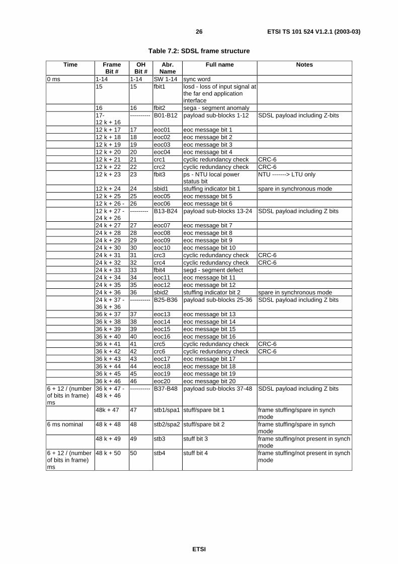
ETSI
ETSI TS 101 524 V1.2.1 (2003-03) 26
Table 7.2: SDSL frame structure
Time Frame Bit #
OH Bit #
Abr. Name
Full name Notes
0 ms 1-14 1-14 SW 1-14 sync word 15 15 fbit1 losd - loss of input signal at
the far end application interface
16 16 fbit2 sega - segment anomaly 17-
12 k + 16 ---------- B01-B12 payload sub-blocks 1-12 SDSL payload including Z-bits
12 k + 17 17 eoc01 eoc message bit 1 12 k + 18 18 eoc02 eoc message bit 2 12 k + 19 19 eoc03 eoc message bit 3 12 k + 20 20 eoc04 eoc message bit 4 12 k + 21 21 crc1 cyclic redundancy check CRC-6 12 k + 22 22 crc2 cyclic redundancy check CRC-6 12 k + 23 23 fbit3 ps - NTU local power
status bit NTU -------> LTU only
12 k + 24 24 sbid1 stuffing indicator bit 1 spare in synchronous mode 12 k + 25 25 eoc05 eoc message bit 5 12 k + 26 - 26 eoc06 eoc message bit 6 12 k + 27 -
24 k + 26 --------- B13-B24 payload sub-blocks 13-24 SDSL payload including Z bits
24 k + 27 27 eoc07 eoc message bit 7 24 k + 28 28 eoc08 eoc message bit 8 24 k + 29 29 eoc09 eoc message bit 9 24 k + 30 30 eoc10 eoc message bit 10 24 k + 31 31 crc3 cyclic redundancy check CRC-6 24 k + 32 32 crc4 cyclic redundancy check CRC-6 24 k + 33 33 fbit4 segd - segment defect 24 k + 34 34 eoc11 eoc message bit 11 24 k + 35 35 eoc12 eoc message bit 12 24 k + 36 36 sbid2 stuffing indicator bit 2 spare in synchronous mode 24 k + 37 -
36 k + 36 ---------- B25-B36 payload sub-blocks 25-36 SDSL payload including Z bits
36 k + 37 37 eoc13 eoc message bit 13 36 k + 38 38 eoc14 eoc message bit 14 36 k + 39 39 eoc15 eoc message bit 15 36 k + 40 40 eoc16 eoc message bit 16 36 k + 41 41 crc5 cyclic redundancy check CRC-6 36 k + 42 42 crc6 cyclic redundancy check CRC-6 36 k + 43 43 eoc17 eoc message bit 17 36 k + 44 44 eoc18 eoc message bit 18 36 k + 45 45 eoc19 eoc message bit 19 36 k + 46 46 eoc20 eoc message bit 20 6 + 12 / (number of bits in frame) ms
36 k + 47 - 48 k + 46
---------- B37-B48 payload sub-blocks 37-48 SDSL payload including Z bits
48k + 47 47 stb1/spa1 stuff/spare bit 1 frame stuffing/spare in synch mode
6 ms nominal 48 k + 48 48 stb2/spa2 stuff/spare bit 2 frame stuffing/spare in synch mode
48 k + 49 49 stb3 stuff bit 3 frame stuffing/not present in synch mode
6 + 12 / (number of bits in frame) ms
48 k + 50 50 stb4 stuff bit 4 frame stuffing/not present in synch mode

ETSI
ETSI TS 101 524 V1.2.1 (2003-03) 27
The following gives a short description of the currently defined overhead bits:
• sync word:
- the synchronization word (SW) enables the SDSL receivers to acquire frame alignment. The synchronization word consists of the following 14-bit sequence: 11111100001100. This sequence shall be passed as a parameter for both upstream and downstream directions during the pre-activation;
- the SW is present in every frame and is the same in both the upstream and downstream directions.
• losd-bit (loss of signal):
- if there is no signal from the application interface, the losd-bit shall be set to ZERO in the next frame towards the far end. Under normal conditions, this bit shall be set to ONE. In four-wire mode, losd on Pair 1 shall carry the primary losd indication. The Pair 2 losd bit shall be a duplicate of the Pair 1 bit.
• sega (segment anomaly):
- the sega-bit shall be used to indicate CRC-errors on the incoming SDSL frames. It is set to ZERO if CRC-errors are detected and to ONE in normal operation.
• segd (segment defect):
- the segd-bit shall be used to indicate loss of synchronization on the incoming SDSL frames. It is set to ZERO if loss of synchronization is detected and to ONE in normal operation.
• eoc-bits (embedded operations channel):
- 20 bits (eoc01...eoc20) are provided as a separate maintenance channel. For a description of codes and the messaging procedure in this channel, see clause 10.5. In four-wire mode, eoc01 - eoc20 on Pair 1 shall carry the primary EOC data. The corresponding Pair 2 eoc bits shall be duplicates of the Pair 1 eoc bits.
• crc-bits:
- the SDSL frame shall have six bits assigned to a Cyclic Redundancy Check (CRC) code. The CRC is generated for each transmitted frame, and then transmitted in the following frame.
The six crc-bits transmitted in the (N + 1)th frame shall be determined as follows:
1) all bits of the Nth frame except the fourteen sync word bits, the six crc-bits and any stuffing bits, for a total of m bits, are used, in order of occurrence, to construct a polynomial in "X" such that bit "0" of the Nth frame is the coefficient of the term Xm-1 and bit m-1 of the Nth frame is the coefficient of the term X0;
2) the polynomial is multiplied by the factor X6, and the result is divided, modulo 2, by the generator polynomial X6 ⊕ X ⊕ 1. The coefficients of the remainder polynomial are used, in order of occurrence, as the ordered set of check bits, crc1 through crc6, for the (N + 1)th frame. The ordering is such that the coefficient of the term X5 in the remainder polynomial is check bit crc1 and the coefficient of the term X0 in the remainder polynomial is check bit crc6;
3) the check bits, crc1 through crc6, contained in a frame are those associated with the content of the preceding frame. When there is no immediately preceding frame, the check bits may be assigned any value.
• ps-bit (power supply bit):
- the power supply bit ps is used to indicate the status of the local power supply in the NTU. The power status bit is set to ONE if power is normal and to ZERO if the power has failed. In four-wire mode, ps on Pair 1 shall carry the primary power status indication. The Pair 2 ps bit shall be a duplicate of the Pair 1 ps bit;
- regenerators shall pass this bit transparently.

ETSI
ETSI TS 101 524 V1.2.1 (2003-03) 28
• sbid (stuff indicator bits):
- (sbid1, sbid2);
- these bits are only needed in plesiochronous mode and are spare in synchronous mode. These stuff indicator bits indicate whether or not a stuffing event has occurred in the frame. Both bits shall be set to 1 if the 4 stuff bits are present at the end of that frame. Both bits shall be set to 0 if there are no stuff bits at the end of the current frame.
• stb (stuffing bits):
- (stb1, stb2, stb3, stb4);
- these bits are only needed in plesiochronous mode and are spare in synchronous mode. They are always used together. Either zero or four stuffing bits are inserted, depending on the relation of the timing. If not used the stuffing bits shall be set to ONE;
- spa (spare bits);
- (spa1, spa2).
These bits are only available in synchronous mode and always used together.
7.1.6 Scrambling method
SDSL transceiver systems use the same self synchronizing scrambling as the 2B1Q transmission system for ISDN-BA as defined in TS 102 080 [2], annex A and HDSL as defined in TS 101 135 [1]. The data stream with the exception of the 14 bits of the sync word and the stuffing bits is scrambled by means of a 23rd-order polynomial prior to encoding.
Table 7.3: Scrambler polynomials
Transmit direction Polynomial Scrambler/Descrambler
NTU → LTU x-23 ⊕ x-18 ⊕ 1 Transmit NTU Receive LTU
LTU → NTU x-23 ⊕ x-5 ⊕ 1 Transmit LTU Receive NTU
NOTE: The sign ⊕ stands for modulo 2 summation.
Figure 7.6 shows block diagrams for the scramblers and the descramblers. It also shows that the binary data stream is recovered in the receiver by applying the same polynomial used for scrambling to the scrambled data.

ETSI
ETSI TS 101 524 V1.2.1 (2003-03) 29
D scrambled (s) data
D unscrambled input ( i) data
D unscrambled output (o ) data
X delay of n bit periods
S
i
O
-n
===
=
X-1 X-1 X
-1X
-1X
-1
D XS-23⋅
X-1 X-1 X
-1X
-1X
-1
D XS-23⋅
DS
DS
X-1 X-1
X-1 X-1 X-1
D XS-23⋅
DS
X-1 X
-1X
-1X
-1X
-1
D XS-23⋅
DS
DO
DO
Di
Di
⊕ = logical exclusive or
⋅ = multiplication
D XS-18⋅
D XS-18⋅
D XS-5⋅
D XS-5⋅
D D D X D XS i S-18
S-23= ⊕ ⋅ ⊕ ⋅
D D D X D XS i S-5
S-23= ⊕ ⋅ ⊕ ⋅
D D X XO S-18 -23= ⋅ ⊕ ⊕( )1
D D X XO S-5 -23= ⋅ ⊕ ⊕( )1
Figure 7.6: Scramblers and descramblers

ETSI
ETSI TS 101 524 V1.2.1 (2003-03) 30
7.1.7 Differential delay buffer
In the optional four-wire mode, it is understood that the characteristics of the two-wire pairs may differ. Differences in wire diameter, insulation type, length, number and length of bridged taps and exposure to impairments may result in differences in transmission time between pairs. It is recommended that such differences in signal transfer delay between the two pairs be limited to a maximum of 50 µs at 150 kHz, corresponding to about 10 km difference in line length between NTU and LTU.
In transceivers supporting four-wire mode, a delay difference buffer shall be implemented to compensate for any difference in total transmission time of the SDSL frames on different pairs. Such delay differences may be due to the pair differences described above, as well as to delays due to signal processing in the SDSL transceivers in the LTU, NTU and possible signal regenerators. The function of this delay difference buffer is to align the SDSL frames so that frames can be correctly reassembled. This buffer shall be capable of absorbing a delay difference of at least 6 symbols + 50 µs at the line side of each SDSL receiver.
7.2 Activation mode frame structure
7.2.1 Activation framer
The format of the activation frame is shown in table 7.4. A Tc or Tr signal shall be generated by repetitively applying
the activation frame information shown in table 7.4 to the scrambler shown in figure 9.1. The activation frame contents shall be constant during the transmission of Tc and Tr The activation frame sync bits are not scrambled, so they shall be
applied directly to the uncoded 2-PAM constellation. The total number of bits in the activation frame is 4 227. The activation frame shall be sent starting with bit 1 and ending with bit 4 227.
In the optional four-wire mode, activation shall proceed in parallel on each of the two-wire pairs.
Table 7.4: Activation frame format
Activation frame bit lsb:msb
Definition
Frame sync for Tc and Tr: 11111001101011, where the left-most bit is sent first in time 1:14
Frame sync for Fc: 11010110011111, where the left-most bit is sent first in time
15:36 Precoder coefficient 1: 22 bit signed two's complement format with 17 bits after the binary point, where the LSB is sent first in time
37:58 Precoder coefficient 2 59:3952 Precoder coefficients 3 - 179 3953:3974 Precoder coefficient 180 3975:3995 Encoder coefficient A: 21 bits where the LSB is sent first in time 3996:4016 Encoder coefficient B: 21 bits where the LSB is sent first in time 4017:4144 Vendor data: 128 bits of proprietary information 4145:4211 Reserved: 67 bits set to logical zeros 4212:4227 CRC: C1 sent first in time, C16 sent last in time
7.2.1.1 Frame sync
The frame sync for Tc and Tr is a 14 bit Barker code. In binary, the code shall be 11111001101011, and shall be sent
from left to right. For Fc, the frame sync shall be 11010110011111, or the reverse of the frame sync for Tc and Tr.
7.2.1.2 Precoder coefficients
The precoder coefficients are represented as 22-bit two's complement numbers, with the 5 most significant bits representing integer numbers from -16 (10000) to +15 (01111), and the remaining 17 bits representing the fractional bits. The coefficients are sent sequentially, starting with coefficient C1 and ending with coefficient CN
(from figure 9.10), and the least significant bit of each coefficient is sent first in time. The minimum number of precoder coefficients shall be 128 and the maximum number shall be 180. If fewer than 180 precoder coefficients are used, the remaining bits in the field shall be set to zero.

ETSI
ETSI TS 101 524 V1.2.1 (2003-03) 31
7.2.1.3 Encoder coefficients
Referring to figure 9.9, the coefficients for the programmable encoder are sent in the following order: a0 is sent first in
time, followed by a1, a2, …, and b20 is sent last in time.
7.2.1.4 Vendor data
These 128 bits are reserved for vendor-specific data.
7.2.1.5 Reserved
These 67 bits are reserved for future use and shall be set to logical zeros.
7.2.1.6 CRC
The sixteen CRC bits (c1 to c16) shall be the coefficients of the remainder polynomial after the message polynomial,
multiplied by D16, is divided by the generating polynomial. The message polynomial shall be composed of the bits of the activation frame, where m0 is bit 15 and m4 196 is bit 4 211 of the activation frame, such that:
CRC(D) = m1(D) D16 mod g(D)
where:
m(D) = m0D4 196 ⊕ m1 D4 195 ⊕ ...⊕ m4 195 D ⊕ m4 196
is the message polynomial,
g(D) = D16 ⊕ D12 ⊕ D5 ⊕ 1
is the generating polynomial,
CRC(D) = c1D15 ⊕ c2D14 ⊕ ...⊕ c15D ⊕ c16
is the CRC check polynomial, ⊕ indicates modulo-2 addition (exclusive OR), and D is the delay operator.
8 Clock architecture
8.1 Tolerance of the line symbol rate At all rates, the transmit symbol clock during data mode from any SDSL device shall be accurate to within ±32 ppm of the nominal frequency. During activation, the LTU shall maintain ±32 ppm accuracy of its transmit symbol clock, but the NTU transmit symbol clock may vary up to ±100 ppm.
8.2 Reference clock architecture Due to the multiple applications and variable bit rates called for in SDSL, a flexible clocking architecture is required. The LTU and NTU symbol clocks are described in terms of their allowed synchronization references. Other clock domains may be accommodated via the supported bit-stuffing mechanism or by using other methods of clock information transport (as in the ISDN-BA narrowband transport option).
The SDSL reference configuration permits the flexibility to provide a symbol clock reference based on the sources shown in figure 8.1. These sources may be chosen independently in the up and downstream directions (with bit stuffing employed as required by the application). The clock accuracy and jitter requirements are specified in a separate clauses or application dependent annexes. It illustrates the clock reference options in the context of a simplified SDSL reference model. Table 8.1 lists the normative synchronization configurations as well as example applications.

ETSI
ETSI TS 101 524 V1.2.1 (2003-03) 32
The clock domain of embedded ISDN-BA channels may be different from that of the data channel. In this case separate stuffing and framing procedures have to be provided for these channels, which shall be described in the relevant application dependent annex.
SDSLTransceiver
Transmit Clk
Transmit Data
Receive Clk
Receive Data
SDSLTransceiver
Transmit Data
Receive Clk
Receive Data
Local oscillator
Receive Symbol Clk
Local oscillator
Network Reference Clk
(Startup Mode only)
NTULTU
TransmitSymbol Clk
TransmitSymbol Clk
Transmit Clk
Figure 8.1: SDSL symbol clock synchronization references
Table 8.1: SDSL symbol clock synchronization configurations
Mode No. LT symbol clock source
NT symbol clock source
Example application Mode
1 Local oscillator Received symbol clock
"Classic" HDSL Plesiochronous
2 Network reference
Received symbol clock
"Classic" HDSL with embedded timing reference
Plesiochronous with timing reference
3a (see note)
Transmit data clock
Received symbol clock
Main application is synchronous transport in both directions
Synchronous
3b (see note)
Transmit data clock
Received symbol clock
Synchronous downstream transport and bit-stuffed upstream is also possible
Downstream: synchronous Upstream: plesiochronous
NOTE: Both modes 3a and 3b are possible with the same clock sources depending on clock tolerances.
8.3 Definitions of clock sources The following definitions shall apply to the clock sources shown in figure 8.1.
8.3.1 Transmit symbol clock
A reference clock from which the actual transmit symbol clock is derived (i.e. the TU's transmit symbol clock is synchronized to this reference).
8.3.2 Local oscillator
A clock derived from an independent local crystal oscillator.
8.3.3 Network reference clock
A primary reference clock derived from the network.

ETSI
ETSI TS 101 524 V1.2.1 (2003-03) 33
8.3.4 Transmit data clock
A clock that is synchronous with the transmitted data at the application interface.
8.3.5 Receive symbol clock
A clock that is synchronous with the downstream received symbols at the SDSL line interface. This clock is used as the transmit symbol clock reference in the NTU.
8.3.6 Receive data clock
A clock that is synchronous with the received data at the application interface.
8.4 Synchronization to clock sources In synchronous mode, the LTU can be synchronized to the transmit data clock or to a network reference clock. If a network reference clock is used, the transmit data clock must be synchronized to the network reference clock. (The various transmit data rates are independent of the reference clock frequency).
When available, the network reference clock shall be either a fundamental 8 kHz network clock or a related reference clock at some multiple of 8 kHz. Such reference clocks are typically 1,544 MHz or 2,048 MHz, although in some applications other frequencies, such as 64 kHz, may be available. These related clocks include implicit 8 kHz timing signals. Selection of a specific network clock reference frequency shall be application dependent.
9 PMD Layer functional characteristics
9.1 Activation This clause describes waveforms at the loop interface and associated procedures during activation mode. The direct specification of the performance of individual receiver elements is avoided when possible. Instead, the transmitter characteristics are specified on an individual basis and the receiver performance is specified on a general basis as the aggregate performance of all receiver elements. Exceptions are made for cases where the performance of an individual receiver element is crucial to interoperability.
In clause 9.1.2 "convergence" refers to the state where all adaptive elements have reached steady state. The declaration of convergence by a transceiver is therefore vendor dependent. Nevertheless, actions based on the state of convergence are specified to improve interoperability.
An optional deactivation and warm start procedure is described in annex D.
9.1.1 Activation PMD reference model
The block diagram of the activation mode PMD layer of an LTU or NTU transmitter is shown in figure 9.1.
ActivationFramer
SpectralShaper
MapperScrambler
d(m)
f(m)
s(m) y(m) z(t)
logicalones
precodercoefficients,
encodercoefficients
output atloop
interface
Figure 9.1: Activation reference model

ETSI
ETSI TS 101 524 V1.2.1 (2003-03) 34
The time index m represents the symbol time, and t represents analogue time. Since activation uses 2-PAM modulation, the bit time is equivalent to the symbol time. The output of the framer is the framed information bits f(m). The output of the scrambler is s(m). Both the framer and the scrambler are contained in the PMS-TC layer and are shown here only for clarity. The output of the mapper is y(m), and the output of the spectral shaper at the loop interface is z(t). d(m) is an initialization signal that shall be logical ones for all m. The modulation format shall be uncoded 2-PAM, with the full symbol rate selected for data mode operation. During activation, the timing reference for the activation signals have a tolerance of ±32 ppm at the LTU and ±100 ppm at the NTU.
In devices supporting the optional four-wire mode, the activation procedure shall be considered as an independent procedure for each pair. Such devices shall be capable of detecting the completion of activation for both pairs and upon completion shall initiate the transmission of user data over both pairs.
9.1.2 Activation sequence
The timing diagram for the activation sequence is given in figure 9.2. The state transition diagram for the activation sequence is given in figure 9.4. Each activation signal in the activation sequence shall satisfy the tolerance values listed in table 9.1.
NOTE: A warm-start procedure is under study for use in systems that can go into a deactivated state, when no communication is going on.
DatarTrCr
tcr
DatacFcTc
tAct
tcrsc
tcrsr
Sr
LTU
NTU
Sc
Figure 9.2: Timing diagram for activation sequence
Figure 9.3 shows the total activation sequence at a high level for SDSL, which includes preactivation and core activation. Included, as an example in the pre-activation phase, are two sessions of handshake per PACC and line probe.
tCore_activation tPre_activation
Data
tAct tp-total
Line Probing Core activationPACC PACC
tAct_Global
Figure 9.3: SDSL total activation sequence

ETSI
ETSI TS 101 524 V1.2.1 (2003-03) 35
The global activation time is the sum of the preactivation and core activation times. Therefore, from figure 9.3,
GlobalActactivationCoreactivationPre ttt ___ ≤+
where tPre activation is the combined duration of the PACC sessions (see clause 9.2) and line probing (see clause 9.2.2),
tCore activation is the core activation duration (see clause 9.1). The values for tAct and tAct_Global are defined in table 9.1.
The value for tp-total is given in table 9.4.
Table 9.1: Tolerance values for activation signals
Signal Parameter Reference Nominal value Tolerance tcr Duration of Cr clause 9.1.2.1 1 × β s (see note 1) ±20 ms tcrsc time from end of Cr to beginning
of Sc clause 9.1.2.2 0,5 s ±20 ms
tcrsr time from end of Cr to beginning
of Sr
clause 9.1.2.3 1,5 × β s (see note 1)
±20 ms
tAct Maximum time from start of Cr to
Datar
15 × β s (see note 1)
tAct_Global Time from start of Initial handshake to Datar (see note 2)
30 s
NOTE 1: β is dependent on bit-rate. β = 1 for n > 12, β = 2 for n ≤ 12. NOTE 2: In the majority of the cases, tAct_Global will be less than 30 s. However, since the definition of the
handshake mechanism in ITU-T Recommendation G.994.1 [16] is outside the scope of the present document, a maximum value tAct_Global cannot be assured.
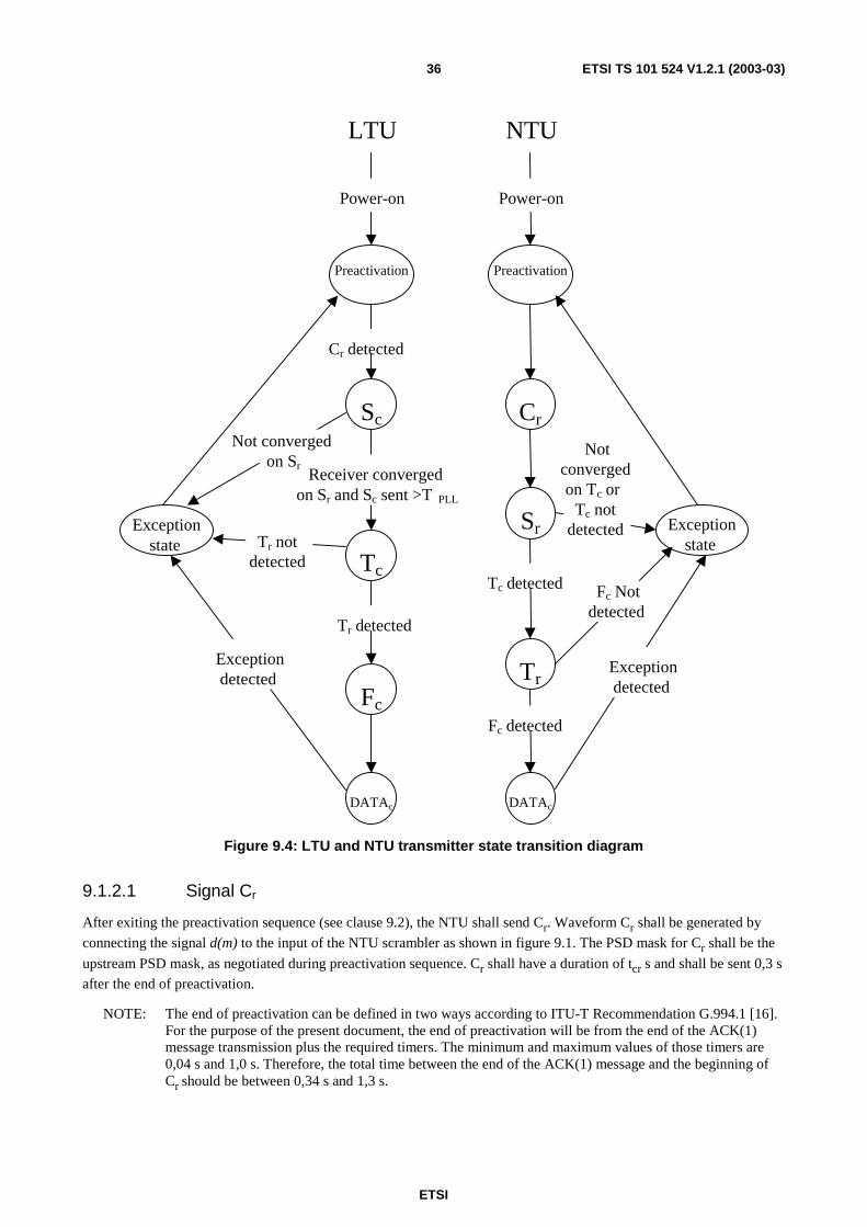
ETSI
ETSI TS 101 524 V1.2.1 (2003-03) 36
Power-on
Sc
LTU
Cr detected
Receiver convergedon Sr and Sc sent >T PLL
Tc
Tr detected
Fc
DATAc
Exceptionstate
Preactivation
Not convergedon Sr
Tr notdetected
Exceptiondetected
Cr
NTU
Sr
Tc detected
Tr
DATAc
Exceptionstate
Preactivation
Notconvergedon Tc or
Tc notdetected
Exceptiondetected
Fc detected
Fc Notdetected
Power-on
Figure 9.4: LTU and NTU transmitter state transition diagram
9.1.2.1 Signal Cr
After exiting the preactivation sequence (see clause 9.2), the NTU shall send Cr. Waveform Cr shall be generated by
connecting the signal d(m) to the input of the NTU scrambler as shown in figure 9.1. The PSD mask for Cr shall be the
upstream PSD mask, as negotiated during preactivation sequence. Cr shall have a duration of tcr s and shall be sent 0,3 s
after the end of preactivation.
NOTE: The end of preactivation can be defined in two ways according to ITU-T Recommendation G.994.1 [16]. For the purpose of the present document, the end of preactivation will be from the end of the ACK(1) message transmission plus the required timers. The minimum and maximum values of those timers are 0,04 s and 1,0 s. Therefore, the total time between the end of the ACK(1) message and the beginning of Cr should be between 0,34 s and 1,3 s.

ETSI
ETSI TS 101 524 V1.2.1 (2003-03) 37
9.1.2.2 Signal Sc
After detecting Cr, the LTU shall send Sc. Waveform Sc shall be generated by connecting the signal d(m) to the input of
the LTU scrambler as shown in figure 9.1. The PSD mask for Sc shall be the downstream PSD mask, as negotiated
during preactivation sequence. Sc shall be sent tcrsc s after the end of Cr. If the LTU does not converge while Sc is
transmitted, it shall enter the exception state (see clause 9.1.2.8).
9.1.2.3 Signal Sr
The NTU shall send Sr, beginning tcrsr s after the end of Cr. Waveform Sr shall be generated by connecting the signal
d(m) to the input of the NTU scrambler as shown in figure 9.1. The PSD mask for Sr shall be the same as for Cr. If the
NTU does not converge and detect Tc while Sr is transmitted, it shall enter the exception state (see clause 9.1.2.8). The
method used to detect Tc is vendor dependent. In timing modes supporting loop timing, waveform Sr and all subsequent
signals transmitted from the NTU shall be loop timed, i.e. the NTU symbol clock shall be locked to the LTU symbol clock.
9.1.2.4 Signal Tc
Once the LTU has converged and has been sending Sc for at least TPLL seconds (see table 9.3), it shall send Tc.
Waveform Tc contains the precoder coefficients and other system information. Tc shall be generated by connecting the
signal f(m) to the input of the LTU scrambler as shown in figure 9.1. The PSD mask for Tc shall be the same as for Sc.
The signal f(m) is the activation frame information as described in clause 9.1.3. If the LTU does not detect Tr while
sending Tc, it shall enter the exception state (see clause 9.1.2.8). The method used to detect Tr is vendor dependent.
9.1.2.5 Signal Tr
Once the NTU has converged and has detected the Tc signal, it shall send Tr. Waveform Tr contains the precoder
coefficients and other system information. Tr shall be generated by connecting the signal f(m) to the input of the NTU
scrambler as shown in figure 9.1. The PSD mask for Tr shall be the same as for Cr. The signal f(m) is the activation
frame information as described in clause 9.1.3. If the NTU does not detect Fc while sending Tr, it shall enter the
exception state (see clause 9.1.2.8). The method used to detect Fc is vendor dependent.
9.1.2.6 Signal Fc
Once the LTU has detected Tr, it shall send Fc. The first bit of the fist Fc frame shall follow contiguously the last bit of
the last Tc frame. Signal Fc shall be generated by connecting the signal f(m) to the input of the LTU scrambler as shown
in figure 9.1. The PSD mask for Fc shall be the same as for Sc. The signal f(m) is the activation frame information as
described in clause 9.1.3 with the following exceptions: the frame sync word shall be reversed in time and the payload information bits shall be set to arbitrary values. The payload information bits correspond to the following fields in table 7.4: Precoder coefficients, Encoder coefficients and Reserved. The CRC shall be calculated on this arbitrary-valued payload. The signal Fc shall be transmitted for exactly two activation frames. As soon as the first bit of
Fc is transmitted, the payload data in the Tr signal shall be ignored.
9.1.2.7 Datac and Datar
Within 200 symbols after the end of the second frame of Fc, the LTU shall send Datac, and the NTU shall send Datar.
These signals are described in clause 9.2. The PSD mask for Datar shall be the same as for Cr, and the PSD mask for
Datac shall be the same as for Sc. There is no required relationship between the end of the activation frame and any bit
within the SDSL data-mode frame. TPayloadValid seconds (see table 9.3) after the end of Fc, the SDSL payload data shall
be valid.

ETSI
ETSI TS 101 524 V1.2.1 (2003-03) 38
9.1.2.8 Exception state
If activation is not achieved within tact (see table 9.1) or if any exception condition occurs, then the exception state shall
be invoked. During the exception state the TU shall be silent for at least tsilence (see table 9.3), then wait for
transmission from the far end to cease, then return to the corresponding initial startup state; the NTU and LTU shall begin preactivation, as per clause 9.2.
9.1.2.9 Exception condition
An exception condition shall be declared during activation if any of the timeouts given in table 9.3 expire or if any vendor-defined abnormal event occurs. An exception condition shall be declared during data mode if the vendor-defined abnormal event occurs. A vendor-defined abnormal event shall be defined as any event that requires loop restart for recovery.
9.1.3 Activation framer
See clause 7.2.1.
9.1.4 Scrambler
The scrambler in the LTU and the NTU transmitters shall operate as shown in figure 7.6. The frame sync bits in the activation frame shall not be scrambled. While the frame sync bits are present at f(n), the scrambler shall not be clocked, and f(n) shall be directly connected to s(n).
9.1.5 Mapper
The output bits from the scrambler s(m) shall be mapped to the an output level y(m) as follows.
Table 9.2: Bit-to-level mapping
Scrambler output s(m) Mapper output level y(m) Data mode index 0 -9/16 0011 1 +9/16 1000
These levels corresponding in the scrambler outputs 0 and 1 shall be identical to the levels in the 16-TC-PAM constellation (see table 9.8) corresponding to indexes 0011 and 1000 respectively.
9.1.6 Spectral shaper
The same spectral shaper shall be used for data mode and activation mode as described in clause 9.3.5.
9.1.7 Timeouts
Tables 9.1 and 9.3 show the system timeouts and their values. tact_Global shall be the maximum time from the start of
initial handshake to the start of Datar. It controls the overall time of the train, including handshake, line probe and
activation. Tact shall be the maximum time from the start of Cr to the start of Datar. TPayloadValid shall be the time
between the start of data mode and when the SDSL payload data is valid (this accounts for settling time, data flushing, frame synchronization, etc). TSilence shall be the minimum time in the exception state where the LTU or NTU are silent
before returning to pre-activation. TPLL shall be the time allocated for the NTU to pull in the LTU timing. The LTU
shall transmit Sc for at least TPLL seconds.

ETSI
ETSI TS 101 524 V1.2.1 (2003-03) 39
Table 9.3: Timeout values
Parameter Name Value Time from start of Datac or Datar to valid SDSL payload data TPayloadValid 1 s
Minimum silence time from exception condition to start of train TSilence 2 s
Time from start of Sc to NTU PLL lock TPLL 5 s
9.2 PMD preactivation sequence This clause describes waveforms at the loop interface and associated procedures during preactivation mode. The direct specification of the performance of individual receiver elements is avoided when possible. Instead, the transmitter characteristics are specified on an individual basis and the receiver performance is specified on a general basis as the aggregate performance of all receiver elements. Exceptions are made for cases where the performance of an individual receiver element is crucial to interoperability.
The Pre-Activation Communication Channel (PACC) shall use the modulation and message structure as described in ITU-T Recommendation G.994.1 [16]. The preactivation communication channel shall allow the selection of the synchronization word described in clause 7.1.5. Annex B specifies the use of ITU-T Recommendation G.994.1 [16] in the context of SDSL.
In the optional four-wire mode, Pair 1 and Pair 2 shall be determined during the preactivation sequence. Pair 1 shall be defined as the pair on which the final G.994.1 transaction is conducted.
9.2.1 PMD preactivation reference model
The reference model of the preactivation mode of an LTU or NTU transmitter is shown in figure 9.5.
SpectralShaper
MapperScramblerd(m) s(m) y(m)
z(t)
logicalones
output atloop
interface
PACCHandshake
Probe
Figure 9.5: Preactivation reference model
The time index m represents the symbol time, and t represents analogue time. Since the probe signal uses 2-PAM modulation, the bit time is equivalent to the symbol time. The output of the scrambler is s(m). The scrambler is contained in the PMS-TC layer and is shown here only for clarity. The scrambler used in the PMD preactivation may differ from the PMS-TC scrambler used in the activation and data mode (see clause 9.2.3). The output of the mapper is y(m) and the output of the spectral shaper at the loop interface is z(t). d(m) is an initialization signal that shall be logical ones for all m. The probe modulation format shall be uncoded 2-PAM, with the symbol rate, spectral shape, duration, and power back-off selected by PACC. Probe results shall be exchanged by PACC.
In the optional four -wire mode, the G.994.1 exchange shall follow the defined procedures for multi-pair operation. In this case, signals Pri and Pci, as described below, shall be sent in parallel on both wire pairs.

ETSI
ETSI TS 101 524 V1.2.1 (2003-03) 40
9.2.2 PMD preactivation sequence description
A typical timing diagram for the preactivation sequence is given in figure 9.6. Each signal in the preactivation sequence shall satisfy the tolerance values listed in table 9.4.
LTU
NTU
tprd tps
tph
tps
tpstpcd
Pr1 Pr2 Pr3
Pc1 Pc2
tprd tprd
tpcd
tprcthp
PACC PACC
Figure 9.6: Typical timing diagram for preactivation sequence
Table 9.4: Timing for preactivation signals
Time Parameter Nominal value Tolerance thp Time from end of handshake to start of remote
probe
0,2 s ±10 ms
tprd Duration of remote probe Selectable from 50 ms to 3,1 s
±10 ms
tps Time separating two probe sequences 0,2 s ±10 ms tprc Time separating last remote and first central
probe sequences 0,2 s ±10 ms
tpcd Duration of central probe Selectable from 50 ms to 3,1 s
±10 ms
tph Time from end of central probe to start of handshake
0,2 s ±10 ms
tp-total Total probe duration, from end of the first G.994.1 session to the start of the second G.994.1 session
10 s maximum
NOTE: Tolerances are relative to the nominal or ideal value. They are not cumulative across the preactivation sequence.
9.2.2.1 Signal Pri
If the optional line probe is selected during the PACC session (see clause 9.2), the NTU shall send the remote probe signal. The symbol rate for the remote probe signal shall be negotiated during the PACC session, and shall correspond to the symbol rate used during activation for the specified data rate. If multiple remote probe symbol rates are negotiated during the PACC session, then multiple probe signals will be generated, starting with the lowest symbol rate negotiated and ending with the highest symbol rate negotiated. Pri is the ith probe signal (corresponding to the ith
symbol rate negotiated). Waveform Pri shall be generated by connecting the signal d(m) to the input of the NTU
scrambler as shown in figure 9.5. The PSD mask for Pri shall be the upstream PSD mask used for signal Cr at the same
symbol rate, and shall be selectable between the PSDs for activating at data rates of 192 kbit/s to 2 304 kbit/s in steps of 64 kbit/s. The duration (tprd) and power back-off shall be the same for all Pri, and shall be negotiated during the PACC
session. The duration shall be selectable between 50 ms and 3,1 s in steps of 50 ms, and the power back-off shall be selectable between 0 dB and 15 dB in steps of 1 dB. The probe signal power back-off can be selected using either the received PACC signal power or a priori knowledge. If no information is available, implementers are encouraged to select a probe power back-off of at least 6 dB. The first remote probe signal shall begin thp seconds after the end of the
PACC session. There shall be a tps second silent interval between successive remote probe signals.
In the optional four-wire mode, Pri shall be sent in parallel on both wire pairs.

ETSI
ETSI TS 101 524 V1.2.1 (2003-03) 41
9.2.2.2 Signal Pci
The LTU shall send the central probe signal tprc seconds after the end of the last remote probe signal. The symbol rate
for the central probe signal shall be negotiated during the PACC session, and shall correspond to the symbol rate used during activation for the specified data rate. If multiple central probe symbol rates are negotiated during the PACC session, then multiple probe signals will be generated, starting with lowest symbol rate negotiated and ending with the highest symbol rate negotiated. Waveform Pci is the ith probe signal (corresponding to the ith symbol rate negotiated).
Waveform Pci shall be generated by connecting the signal d(m) to the input of the LTU scrambler as shown in
figure 9.5. The PSD mask for Pci shall be the downstream PSD mask used for signal Sc at the same symbol rate, and
shall be selectable between the PSDs for activating at data rates of 192 kbit/s to 2 304 kbit/s in steps of 64 kbit/s. The duration (tpcd) and power back-off shall be the same for all Pci, and shall be negotiated during the PACC session. The
duration shall be selectable between 50 ms and 3,1 s in steps of 50 ms, and the power back-off shall be selectable between 0 dB and 15 dB in steps of 1 dB. The probe signal power back-off can be selected using either the received PACC signal power or a priori knowledge. If no information is available, implementers are encouraged to select a probe power back-off of at least 6 dB. There shall be a tps silent interval between successive central probe signals, and there
shall be a tph second silent interval between the last central probe signal and the start of the following PACC session.
In the optional four-wire mode, Pci shall be sent in parallel on both wire pairs.
9.2.3 Scrambler
The scrambler used in the PMD preactivation has the same basic structure as the data mode scrambler, but can have different scrambler polynomial. During the PACC session, the scrambler polynomial for each probe sequence is selected by the receiver from the set of allowed scrambler polynomials listed in table 9.5. The transmitter shall support all the polynomials in table 9.5. During PMD preactivation, the transmit scrambler shall use the scrambler polynomial selected by the receiver during the PACC session. The scrambler shall be initialized to all zero.
Table 9.5: Preactivation scrambler polynomials
Index LTU polynomial NTU polynomial 0 ( ) ( ) ( ) ( )ndnsnsns ⊕−⊕−= 235 )()23()18()( ndnsnsns ⊕−⊕−=
1 )()1()( ndnsns ⊕−= )()1()( ndnsns ⊕−=
2 )()5()2()( ndnsnsns ⊕−⊕−= )()5()3()( ndnsnsns ⊕−⊕−=
3 )()6()1()( ndnsnsns ⊕−⊕−= )()6()5()( ndnsnsns ⊕−⊕−=
4 )()7()3()( ndnsnsns ⊕−⊕−= )()7()4()( ndnsnsns ⊕−⊕−=
5
)()8(
)4()3()2()(
ndns
nsnsnsns
⊕−⊕−⊕−⊕−=
)()8(
)6()5()4()(
ndns
nsnsnsns
⊕−⊕−⊕−⊕−=
9.2.4 Mapper
The output bits from the scrambler s(m), shall be mapped to the output level y(m), as described in clause 9.1.5.
9.2.5 Spectral shaper
The same spectral shaper shall be used for data mode and activation mode as described in clause 9.3.5.

ETSI
ETSI TS 101 524 V1.2.1 (2003-03) 42
9.2.6 Power Back-Off
In order to save power and reduce ingress to other xDSL transmission systems, power back-off shall be implemented. The selected power back-off value shall be communicated through the use of parameter selections during the preactivation procedure. The power back-off value shall be selected to meet the requirements shown in table 9.6, which shall be understood as a minimum requirement.
The power back-off calculations are based on "Estimated Power Loss" (EPL), which is defined as:
EPL = Transmit power - Estimated receive power evaluated for the data mode PSD.
No explicit specification is given herein for the method of calculating "Estimated Receive Power". Depending upon the application, this value may be determined based on line probe results, a priori knowledge or levels of tones used during the preactivation procedure.
The power back-off that is applied shall be no less than the default power back-off, and it shall not exceed the maximum power back-off value.
Table 9.6: Required power back-off values
Estimated power loss/dB Maximum power back-off/dB Default power back-off/dB EPL ≥ 6 31 0
5 ≤ EPL < 6 31 1 4 ≤ EPL < 5 31 2 3 ≤ EPL < 4 31 3 2 ≤ EPL < 3 31 4 1 ≤ EPL < 2 31 5 0 ≤ EPL < 1 31 6
9.2.7 PMMS target margin
PMMS target margin is used by the receiver to determine if a data rate can be supported with this margin under current noise and/or reference worst-case noise. A data rate may be included in the capabilities list resulting from line probe only if the estimated SNR associated with that data rate minus the SNR required for BER = 10-7 is greater than or equal to target margin in dB. If both worst-case target margin and current-condition target margin are specified, then the capabilities exchanged shall be the intersection of data rates calculated using each noise condition separately.
The use of negative target margins with respect to reference worst-case noise corresponds to reference noise with fewer disturbers. This may be applicable when the number of disturbers is known to be substantially fewer than specified by the reference worst-case noise. Use of negative target margins with respect to current-conditions is not advised. Use of the current-condition target margin mode may result in retrains if the noise environment changes significantly.
If the optional line probe is selected during the G.994.1 session, the receiver shall use the negotiated target margin. If worst-case PMMS target margin is selected, then the receiver shall assume the disturbers of table 9.7 to determine if a particular rate can be supported. Reference crosstalk shall be computed using the cable crosstalk models of clause 12.5.2, assuming infinite loop length so that FEXT components are ignored and NEXT is independent of loop length. The reference crosstalk specified in this clause may not be representative of worst-case conditions in all networks. Differences between crosstalk environments may be compensated by adjusting the target margin.
Table 9.7: Reference disturbers used during PMMS for worst-case target margin
Rate (kbit/s) PSD (direction) Reference disturber all Symmetric (US/DS) 49 SDSL 2 048 Asymmetric (US) 49 SDSL-SYM with fsym = 685 333 Hz 2 048 Asymmetric (DS) 49 SDSL-SYM with fsym = 685 333 Hz 2 304 Asymmetric (US) 49 SDSL-SYM with fsym = 770 667 Hz 2 304 Asymmetric (DS) 49 SDSL-SYM with fsym = 770 667 Hz

ETSI
ETSI TS 101 524 V1.2.1 (2003-03) 43
9.3 Data mode This clause describes the waveform at the line interface during data mode given the input bit stream from the TC layer.
9.3.1 Data mode PMD reference model
The block diagram of the data mode PMD layer of an LTU or NTU transmitter is shown in figure 9.7.
Scrambler UC-PAMEncoder
SpectralShaper
s(n) y(m) z(t)
inputfrom TClayer
outputat lineinterface
f(n)ChannelPrecoder
x(m)
Figure 9.7: Data mode PMD reference model
The time index n represents the bit time, the time index m represents the symbol time, and t represents analogue time. The input from the TC layer is f(n), s(n) is the output of the scrambler. The scrambler is contained in the PMS-TC layer and is shown here only for clarity. x(m) is the output of the UC-PAM (Ungerboeck Coded Pulse Amplitude Modulation) encoder, y(m) is the output of the channel precoder, and z(t) is the analogue output of the spectral shaper at the line interface. When transferring K information bits per one-dimensional PAM symbol, the symbol duration is K times the bit duration, so the K values of n for a given value of m are mK, mK + 1, …, mK + K - 1.
In the optional four-wire mode, two separate PMD sublayers are active - one for each wire pair. In this case, n represents the bit time for each wire pair rather than the aggregate system line rate.
9.3.1.1 PMD rates
The transmission is 16 UC-PAM. There are 3 data bits and 1 redundant bit transmitted each symbol. The TU shall support a line rate of (n × 64 + i × 8 + 8) kbit/s, where n is an integer value from 3 to 36 and i is an integer value from 0 to 7. The tolerance on the symbol rate shall be ±32 ppm.
9.3.2 Scrambler
The scrambler in the LTU and the NTU transmitters are described in clause 7.1.6. While the frame sync bits and stuff bits are present at f(n), the scrambler shall not be clocked and f(n) shall be directly connected to s(n).
9.3.3 UC-PAM encoder
The block diagram of the UC-PAM encoder is shown in figure 9.8. The serial bit stream from the scrambler s(n) shall be converted to a K-bit parallel word at the mth symbol time, then processed by the convolutional encoder. The resulting K + 1-bit word shall be mapped to one of 2K + 1 pre-determined levels forming x(m).

ETSI
ETSI TS 101 524 V1.2.1 (2003-03) 44
ConvolutionalEncoder
Serial toParallel
Y1(m)
Y2(m)
Y0(m)
YK(m)s(mK+K-1)=XK(m)
s(mK+0)=X1(m)
s(mK+1)=X2(m) x(m)Mappers(n)
Figure 9.8: Block diagram of the UC-PAM encoder
9.3.3.1 Serial-to-parallel converter
The serial bit stream from the scrambler, s(n), shall be converted to a K-bit parallel word X1(m) = s(mK), X2(m) = s(mK + 1), …, XK(m) = s(mK + K - 1) at the mth symbol time, where X1(m) is the first in time.
9.3.3.2 Convolutional encoder
Figure 9.9 shows the feed forward non-systematic convolutional encoder, where Ts is a delay of one symbol time, "⊕ "
is binary exclusive-OR, and "⊗ " is binary AND. X1(m) shall be applied to the convolutional encoder, Y1(m) and Y0(m)
shall be computed, then X1(m) shall be shifted into the shift register.
a1a0
TsTsTs
a2
...
...
...a19 a20
b1
Y0(m)
Y1(m)
X1(m-20)X1(m-19)X1(m-1)X1(m)
b0 b2 b19 b20
Figure 9.9: Block diagram of the convolutional encoder
The binary coefficients aI and bI shall be passed to the encoder from the receiver during the activation phase specified in
clause 9.1. A numerical representation of these coefficients is A and B, where:
A = a20•220 + a19•219 + a18•218 + … + a0•20
and:
B = b20•220 + b19•219 + b18•218 + … + b0•20
The specific choice of Ungerboeck code is vendor specific. The Ungerboeck code shall be chosen such that the system performance requirements are satisfied.

ETSI
ETSI TS 101 524 V1.2.1 (2003-03) 45
9.3.3.3 Mapper
For K = 3, the bits Y3(m), Y2(m), Y1(m), and Y0(m) shall be mapped to a level x(m) as specified in table 9.8.
Table 9.8: Data mode bit-to-level mapping
Trellis encoder output, Y3(m) Y2(m) Y1(m) Y0(m)
Level x(m) (see note)
0000 -15/16 0001 -13/16 0010 -11/16 0011 -9/16 0100 -7/16 0101 -5/16 0110 -3/16 0111 -1/16 1100 1/16 1101 3/16 1110 5/16 1111 7/16 1000 9/16 1001 11/16 1010 13/16 1011 15/16
NOTE: The values are fractions of the value 1 as defined in clause 9.3.4.
9.3.4 Channel precoder
The block diagram of channel precoder is shown in figure 9.10, where Ts is a delay of one symbol time.
-
+Modulo
Precoder filter
u(m)
v(m)
y(m)x(m)
XX X X
…Ts Ts Ts Ts
C 1C 2C N-1C N
y(m-N) y(m-2) y(m-1)
Figure 9.10: Block diagram of the channel precoder
The coefficients Ck of the precoder filter shall be transferred to the channel precoder as described in clause 7.2.1.2. The
output of the precoder filter v(m) shall be computed as follows:
v(m) C y(m k)kk 1
N
= −=∑
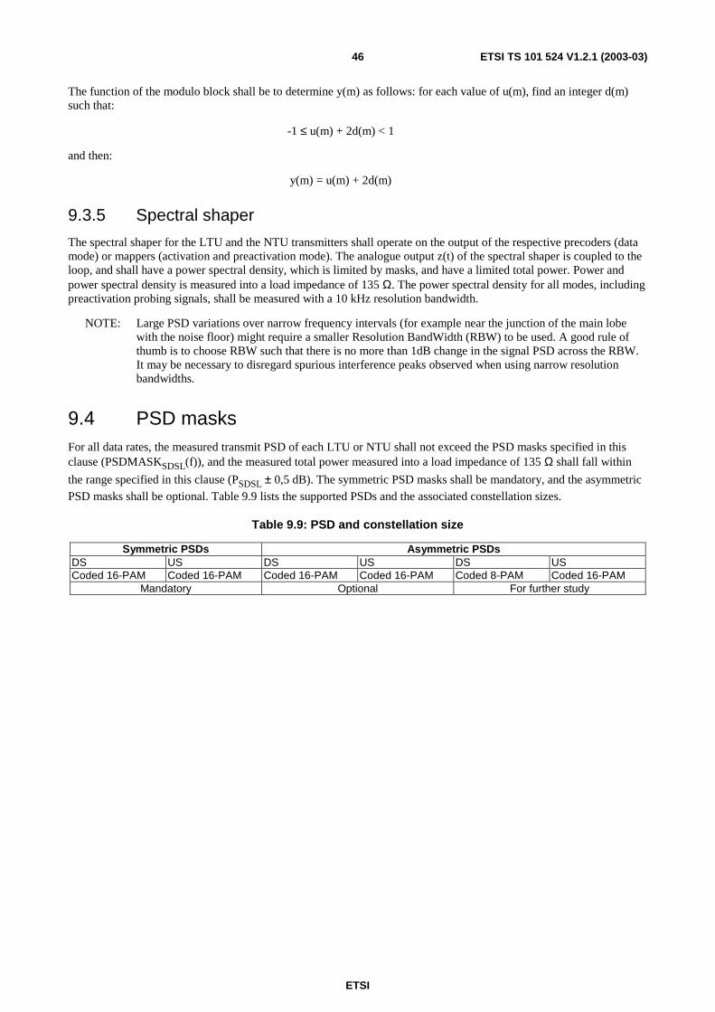
ETSI
ETSI TS 101 524 V1.2.1 (2003-03) 46
The function of the modulo block shall be to determine y(m) as follows: for each value of u(m), find an integer d(m) such that:
-1 ≤ u(m) + 2d(m) < 1
and then:
y(m) = u(m) + 2d(m)
9.3.5 Spectral shaper
The spectral shaper for the LTU and the NTU transmitters shall operate on the output of the respective precoders (data mode) or mappers (activation and preactivation mode). The analogue output z(t) of the spectral shaper is coupled to the loop, and shall have a power spectral density, which is limited by masks, and have a limited total power. Power and power spectral density is measured into a load impedance of 135 Ω. The power spectral density for all modes, including preactivation probing signals, shall be measured with a 10 kHz resolution bandwidth.
NOTE: Large PSD variations over narrow frequency intervals (for example near the junction of the main lobe with the noise floor) might require a smaller Resolution BandWidth (RBW) to be used. A good rule of thumb is to choose RBW such that there is no more than 1dB change in the signal PSD across the RBW. It may be necessary to disregard spurious interference peaks observed when using narrow resolution bandwidths.
9.4 PSD masks For all data rates, the measured transmit PSD of each LTU or NTU shall not exceed the PSD masks specified in this clause (PSDMASKSDSL(f)), and the measured total power measured into a load impedance of 135 Ω shall fall within
the range specified in this clause (PSDSL ± 0,5 dB). The symmetric PSD masks shall be mandatory, and the asymmetric PSD masks shall be optional. Table 9.9 lists the supported PSDs and the associated constellation sizes.
Table 9.9: PSD and constellation size
Symmetric PSDs Asymmetric PSDs DS US DS US DS US Coded 16-PAM Coded 16-PAM Coded 16-PAM Coded 16-PAM Coded 8-PAM Coded 16-PAM
Mandatory Optional For further study

ETSI
ETSI TS 101 524 V1.2.1 (2003-03) 47
9.4.1 Symmetric PSD masks
For all values of framed data rate available in the LTU or NTU, the following set of PSD masks (PSDMASKSDSL(f)) shall be selectable:
=(f)PSDMASKSDSL
[W/Hz] 10
f
f1
1
f
fπ
f
fπsin
f
1K10 (f) 10
dB(f)MaskOffset
Order2
3dB
2
sym
2
sym
sym
SDSL10
PBO-
1 ×
+
×
×××= ×sR
P
intff <
MHz5,1ff int ≤≤
dBm 50- of windowMHz] 1 f [f, ain power maximumpeak with dBm/Hz -90(f)P 3 += maxfMHz 1,5 f≤<
where:
PBO = the Power Back-Off value in dB, as defined in clause 9.2.6
Ksdsl, fsym, f3dB and Order are defined in table 9.10
f = frequency in Hz
Rs= 135 Ω
≥
<−×+=3dB
3dB3dB
3dB
ff[dB],1
ff[dB],f
ff0,41
dB(f)MaskOffset
fint = lowest frequency above f3dB where the expressions for P1(f) and P2(f) intersect
fmax = 11,040 MHz
Table 9.10: Symmetric PSD parameters
Payload data rate, R (bit/s)
KSDSL
(V2)
Order fsym (Hz)
f3dB (Hz)
PSDSL (dBm)
R < 2 048 x 103 bit/s 7,86 6 (R + 8 000 bit/s) / (3bit) 1,0 x fsym / 2 P1(R) ≤ PSDSL ≤ 13,5 dBm
R ≥ 2 048 x 103 bit/s 9,90 6 (R + 8 000 bit/s) / (3bit) 1,0 x fsym / 2 14,5 dBm
P1(R) with R given in bit/s- is defined as follows:
P1(R) = 0,3486 log2 (R + 8 000) + 6,06
For 0 dB power back-off, the measured transmit power measured into a load impedance of 135 Ω shall fall within the range PSDSL ± 0,5 dB where PSDSL is defined in table 9.10. For power back-off values other than 0 dB, the measured
transmit power measured into a load impedance of 135 Ω shall fall within the range PSDSL ± 0,5 dB minus the power
back-off value in dB. The measured transmit PSD measured into a load impedance of 135 Ω shall remain below PSDMASKSDSL(f). The inband PSD for 0 MHz < f < 1,5 MHz shall be measured with a 10 kHz resolution bandwidth (see note in clause 9.3.5).

ETSI
ETSI TS 101 524 V1.2.1 (2003-03) 48
Figure 9.11 shows the PSD masks with 0 dB power back-off for data rates of 256 kbit/s, 512 kbit/s, 768 kbit/s, 1 536 kbit/s, 2 048 kbit/s and 2 304 kbit/s plus 8 kbit/s of overhead.
0 0,2 0,4 0,6 0,8 1 -110
-100
-90
-80
-70
-60
-50
-40
-30
Frequency (MHz)
PS
D (
dBm
/Hz)
Figure 9.11: Symmetric PSD masks for 0 dB power back-off

ETSI
ETSI TS 101 524 V1.2.1 (2003-03) 49
The equation for the nominal PSD measured at the terminals is:
=(f)NominalPSDSDSL
[W/Hz] ff
f
f
f1
1
f
fπ
f
fπsin
f
1K10 (f)
2c
2
2
Order2
3dB
2
sym
2
sym
sym
SDSL10
PBO-
1 +×
+
×
×××= ×sR
P
intff <
MHz5,1ff int ≤≤
dBm 50- of windowMHz] 1 f [f, ain power maximumpeak with dBm/Hz -90(f)P 3 += maxfMHz 1,5 f≤<
where:
PBO = the Power Back-Off value in dB, as defined in clause 9.2.6
Ksdsl, fsym, f3dB and Order are defined in table 9.10
f = frequency in Hz
Rs= 135 Ω
fc is the transformer cut-off frequency, assumed to be 5 kHz
fint = lowest frequency above f3dB where the expressions for P1(f) and P2(f) intersect
fmax = 11,040 MHz
The inband PSD for 0 MHz < f < 1,5 MHz shall be measured with a 10 kHz resolution bandwidth (see note in clause 9.3.5). Figure 9.12 shows the nominal transmit PSDs with 13,5 dBm power for data rates of 256 kbit/s, 512 kbit/s, 768 kbit/s, 1 536 kbit/s, 2 048 kbit/s and 2 304 kbit/s plus 8 kbit/s of overhead.
NOTE 1: The nominal PSD is given for information only.

ETSI
ETSI TS 101 524 V1.2.1 (2003-03) 50
0 0,2 0,4 0,6 0,8 1 -110
-100
-90
-80
-70
-60
-50
-40
-30
Frequency (MHz)
PS
D (
dBm
/Hz)
Figure 9.12: Nominal symmetric PSDs for 0 dB power back-off
NOTE 2: The out of band value (P3(f)) is under study and may change to reflect a common value for all DSL systems.
9.4.2 Asymmetric 2 048 kbit/s and 2 304 kbit/s PSD masks
The asymmetric PSD mask set specified in this clause shall optionally be supported for the 2 048 kbit/s and the 2 304 kbit/s payload data rate.
NOTE 1: Power and power spectral density are measured into a load impedance of 135 Ω.
NOTE 2: Other optional asymmetric PSD masks are for further study.

ETSI
ETSI TS 101 524 V1.2.1 (2003-03) 51
For the 2 048 kbit/s and the 2 304 kbit/s payload data rates available in the LTU or NTU, the following set of PSD masks (PSDMASKSDSL(f)) shall be selectable:
=(f)PSDMASKSDSL
[W/Hz] 10
f
f1
1
f
fπ
f
fπsin
f
1K10 (f) 10
dB(f)MaskOffset
Order2
3dB
2
x
2
x
x
SDSL10
PBO-
1 ×
+
×
×××= ×sR
P
intff <
MHz5,1ff int ≤≤
dBm 50- of windowMHz] 1 f [f, ain power maximumpeak with dBm/Hz -90(f)P 3 += maxfMHz 1,5 f≤<
PBO = the Power Back-Off value in dB, as defined in clause 9.2.6
Ksdsl, fx, f3dB and Order are defined in table 9.11
f = frequency in Hz
Rs = 135 Ω
≥
<−×+=3dB
3dB3dB
3dB
ff[dB],1
ff[dB],f
ff0,41
dB(f)MaskOffset
fint = lowest frequency above f3dB where the expressions for P1(f) and P2(f) intersect
fmax = 11,040 MHz
Table 9.11: Asymmetric PSD parameters
Payload data rate (bit/s)
Transmitter KSDSL
(V2)
Order fx (Hz)
f3dB (Hz)
PSDSL (dBm)
2 048 x 103 bit/s LTU 16,86 7 1 370 667 Hz 548 267 Hz 16,25 dBm 2 048 x 103 bit/s NTU 15,66 7 685 333 Hz 342 667 Hz 16,50 dBm
2 304 x 103 bit/s LTU 12,48 7 1 541 333 Hz 578 000 Hz 14,75 dBm
2 304 x 103 bit/s NTU 11,74 7 770 667 Hz 385 333 Hz 15,25 dBm
For 0 dB power back-off, the measured transmit power measured into a load impedance of 135 Ω shall fall within the range PSDSL ± 0,5 dB where PSDSL is defined in table 9.11. For power back-off values other than 0 dB, the measured
transmit power measured into a load impedance of 135 Ω shall fall within the range PSDSL ± 0,5 dB minus the power
back-off value in dB. The measured transmit PSD measured into a load impedance of 135 Ω shall remain below PSDMASKSDSL(f). The inband PSD for 0 MHz < f < 1,5 MHz shall be measured with a 10 kHz resolution bandwidth (see note in clause 9.3.5).
Figure 9.13 shows the asymmetric PSD masks with 0 dB power back-off for payload data rates of 2 048 kbit/s and 2 304 kbit/s.

ETSI
ETSI TS 101 524 V1.2.1 (2003-03) 52
0 0,2 0,4 0,6 0,8 1 -110
-100
-90
-80
-70
-60
-50
-40
-30
Frequency (MHz)
PS
D (
dBm
/Hz)
Figure 9.13: Asymmetric PSD masks for 0 dB power back-off
The equation for the nominal PSD measured at the terminals is:
=(f)NominalPSDSDSL
[W/Hz] ff
f
f
f1
1
f
fπ
f
fπsin
f
1K10 (f)
2c
2
2
Order2
3dB
2
x
2
x
x
SDSL10
PBO-
1 +×
+
×
×××= ×sR
P
intff <
MHz5,1ff int ≤≤
dBm 50- of windowMHz] 1 f [f, ain power maximumpeak with dBm/Hz -90(f)P 3 += maxfMHz 1,5 f≤<
where:
PBO = the Power Back-Off value in dB, as defined in clause 9.2.6
Ksdsl, fx, f3dB and Order are defined in table 9.11
f = frequency in Hz
Rs= 135 Ω
fc is the transformer cut-off frequency, assumed to be 5 kHz
fint = lowest frequency above f3dB where the expressions for P1(f) and P2(f) intersect
fmax = 11,040 MHz

ETSI
ETSI TS 101 524 V1.2.1 (2003-03) 53
The inband PSD for 0 MHz < f < 1,5 MHz shall be measured with a 10 kHz resolution bandwidth (see note in clause 9.3.5). Figure 9.14 shows the nominal transmit PSDs with 0 dB power back-off for payload data rates of 2 048 kbit/s and 2 304 kbit/s.
NOTE 3: The nominal PSD is given for information only.
0 0,2 0,4 0,6 0,8 1 -110
-100
-90
-80
-70
-60
-50
-40
-30
Frequency (MHz)
PS
D (
dBm
/Hz)
Figure 9.14: Nominal asymmetric PSDs for 0 dB power back-off
NOTE 4: The out of band value (P3(f)) is under study and may change to reflect a common value for all DSL systems.
10 Operation and maintenance
10.1 Management reference model
LTU
C-side
NTU
R-side REG-C
REG
REG-R REG-C
REG
REG-R
TECentralOffice
equipment
SDSLsegment
SDSLsegment
SDSLsegment
applicationspecific
applicationspecific
SDSL span
user data path
Figure 10.1: Management reference model

ETSI
ETSI TS 101 524 V1.2.1 (2003-03) 54
Figure 10.1 shows the management reference model for user data transport over SDSL. This example includes two regenerator units for informative purposes. The presence of two regenerators is not intended to be a requirement or limit. An SDSL segment is characterized by a metallic transmission medium utilizing an analogue coding algorithm, which provides both analogue and digital performance monitoring at the segment entity. An SDSL segment is delimited by its two end points, known as segment terminations. An SDSL segment termination is the point at which the analogue coding algorithms end and the subsequent digital signal is monitored for integrity.
All SDSL performance monitoring data is transported over the eoc. The fixed indicator bits in the SDSL frame losd, sega, segd and ps are used for rapid communication of interface or SDSL segment defects, which may lead to protection switching. In addition, the fixed indicator bits may be used for rapid alarm filtering SDSL segment failures.
10.2 SDSL primitives and failures
10.2.1 Cyclic Redundancy Check anomaly (CRC)
A CRC anomaly shall be declared when the crc-bits generated locally on the data in the received SDSL frame do not match the crc-bits (crc1 - crc6) received from the transmitter. A CRC anomaly only pertains to the frame over which it was declared.
10.2.2 SEGment Anomaly (SEGA)
An upstream segment anomaly shall be declared when any signal regenerator declares a CRC anomaly for an SDSL frame moving in the direction from NTU to LTU. A downstream segment anomaly shall be declared when any signal regenerator declares a CRC anomaly for an SDSL frame moving in the direction from LTU to NTU. A segment anomaly indicates that a regenerator operating on a segment has received corrupted data and therefore the regenerated data is unreliable. The purpose of segment anomaly is to ensure internal SDSL PMD integrity; it is not intended to be reported to an external management entity. A segment anomaly is indicated via the sega-bit in the SDSL frame.
10.2.3 Loss of Sync Word defect (LOSW defect)
This defect is indicated in the eoc through message ID 140 and from regenerators additionally through segd-bit.
In plesiochronous mode, a LOSW defect shall be declared when at least 3 consecutive received frames contain one or more errors in the framing bits. The term framing bits shall refer to that portion of Sync word, stuffing bits and stuff indicator bits, which are used for frame synchronization. A LOSW defect shall be cleared when at least 2 consecutive received frames contain no errors in the framing bits.
In synchronous mode, a LOSW defect shall be declared when at least 3 consecutive received frames contain one or more bit errors in the Frame Sync Word. A LOSW defect shall be cleared when at least 2 consecutive received frames contain no errors in the frame sync word.
10.2.4 SEGment Defect (SEGD)
An upstream segment defect shall be declared when any signal regenerator declares a LOSW defect for data moving in the direction from NTU to LTU. A downstream segment defect shall be declared when any signal regenerator declares a LOSW defect for data moving in the direction from LTU to NTU. A segment defect indicates that a regenerator has lost SDSL synchronization and therefore the regenerated data is unavailable. A segment defect shall be cleared when all regenerators have no LOSW defects. This primitive is typically reported to an external management entity and is used to ensure timely protection switching, alarm filtering, etc. A segment defect is indicated via the segd-bit in the SDSL frame.
10.2.5 Loop Attenuation Defect
A Loop Attenuation Defect shall be declared when the observed Loop Attenuation is at a level higher than the configured threshold (see clause 10.5.5.7.5).

ETSI
ETSI TS 101 524 V1.2.1 (2003-03) 55
10.2.6 SNR Margin Defect
An SNR Margin Defect shall be declared when the observed SNR Margin is at a level lower than the configured threshold (see clause 10.5.5.7.5). SNR Margin is defined as the maximum dB increase in equalized noise or the maximum dB decrease in equalized signal that a system can tolerate and maintain a BER of 10-7.
NOTE: The SNR Margin assumes additive Gaussian noise.
10.2.7 LOss of Sync Word Failure (LOSW failure)
This defect is indicated in the eoc through message ID 141 and from regenerators additionally through segd-bit.
An LOSW failure shall be declared after 2,5 s ± 0,5 s of contiguous LOSW defect. The LOSW failure shall be cleared when the LOSW defect is absent between 2 s and 20 s. The minimum hold time for indication of LOSW failure shall be 2 s.
10.2.8 Loss of local power
The NTU shall indicate loss of local power to the LTU through ps-bit. The NTU shall be able to send the ps-bit in at least 1 and preferably 3 consecutive frames after losing local power. If the ps-bit is set for less than three frames, it is up to the application at the LTU layer to determine the validity of the message.
10.2.9 Loss Of Signal (LOS)
The Loss Of Signal flag (LOS = ONE) indicates that no signal is detected on the line. LOS = ZERO indicates that a signal has been detected. The LOS at the NTU side is set to zero as soon as the Sc signal is detected. The LOS at the
LTU side is set to zero as soon as the Sr signal is detected. LOS at the line side of the LTU, NTU or REG leads to a deactivation of the respective path after 2 s and therefore always results in an LOS message from the SDSL core to the Operation & Maintenance (O&M) functional block in the LTU. The LTU O&M unit cannot determine however the location of the fault.
10.3 SDSL line related performance parameters
10.3.1 Code Violation (CV)
The SDSL parameter Code Violation is defined as a count of the SDSL CRC anomalies occurring during the accumulation period. This parameter is subject to inhibiting - see clause 10.3.6.
10.3.2 Errored Second (ES)
The SDSL parameter Errored Second is defined as a count of 1 s intervals during which one or more CRC anomalies are declared and/or one or more LOSW defects are declared. This parameter is subject to inhibiting - see clause 10.3.6.
10.3.3 Severely Errored Second (SES)
The SDSL parameter Severely Errored Second is defined as a count of 1 s intervals during which at least 50 CRC anomalies are declared or one or more LOSW defects are declared. (50 CRC anomalies during a 1 s interval is equivalent to a 30 % errored frame rate for a nominal frame length.) This parameter is subject to inhibiting - see clause 10.3.6.
10.3.4 LOSW Second (LOSWS)
The SDSL parameter LOSW Second is defined as a count of 1 s intervals during which one or more SDSL LOSW defects are declared.

ETSI
ETSI TS 101 524 V1.2.1 (2003-03) 56
10.3.5 UnAvailable Second (UAS)
The SDSL parameter Unavailable Second is a count of 1 s intervals for which the SDSL line is unavailable. The SDSL line becomes unavailable at the onset of 10 contiguous SESs. The 10 SESs are included in the unavailable time. Once unavailable, the SDSL line becomes available at the onset of 10 contiguous seconds with no SESs. The 10 s with no SESs are excluded from unavailable time.
10.3.6 Inhibiting rules
- UAS parameter counts shall not be inhibited;
- ES and SES shall be inhibited during UAS. Inhibiting shall be retroactive to the onset of unavailable time and shall end retroactively to the end of unavailable time;
- the CV parameter shall be inhibited during SES.
Further information on inhibiting rules and how ES and SES are decremented can be found in IETF/RFC 2495 [21].
10.4 Performance data storage Performance history for all SDSL segment endpoints shall be maintained at the LTU. In order to support SDSL performance history storage at the LTU, each SDSL network element shall monitor performance and maintain a modulo counter for each performance parameter that is specified in clauses 10.5.5.7.15 and 10.5.5.7.16, as appropriate. No initialization of these modulo counters is specified or necessary. By comparing the current reading of the modulo counter with the previous reading stored in memory, the data base manager in the LTU can determine the number of counts to add to the appropriate performance history bin. (Note that the number of counts may decrease under some fault conditions - see clause 10.3 for additional information.) The modulo counters are reported in the SDSL Performance Status Messages (see clauses 10.5.5.7.15 and 10.5.5.7.16).
In order to monitor ES and SES, each SDSL element shall maintain a 1 s timer and an 8 bit modulo counter for each receiver. (An NTU or LTU shall have 1 counter. A signal regenerator shall have 2 counters.) The corresponding counter shall be incremented for every ES or SES that is declared. The LTU shall collect performance history by polling each SDSL network element with a time interval that precludes overflow of the modulo counter. The LTU should maintain performance history registers for each SDSL segment endpoint. The performance history registers shall include the total collected counts for the current 15 minute period, 32 previous 15 minute periods, current 24 hour period, and 7 previous 24 hour periods.
10.5 SDSL embedded operations channel (eoc)
10.5.1 eoc management reference model
The LTU shall maintain a management information database for external access by network management or via craft terminal interface.
Optionally, the NTU may maintain a management information database, which can be locally accessed (through a craft terminal interface). This is particularly useful when the LTU, due to fault conditions, is unreachable via the eoc.
Access to the management information database from craft terminal interfaces on attached units shall be provided through a virtual terminal interface.

ETSI
ETSI TS 101 524 V1.2.1 (2003-03) 57
10.5.2 eoc overview and reference model
The eoc allows terminal units to maintain information about the span. There are two basic flows of data, differentiated by which terminal unit initiates the data flow (and subsequently stores the information for external access.) The data flow initiating from the LTU is mandatory. The data flow initiating from the NTU is optional, but all units must respond to requests in either direction of data flow. In all cases the "master database" shall be stored at the LTU and all conflicts shall be resolved in favour of the LTU (i.e. the information at the LTU takes precedence). The data flows are illustrated in table 10.1 for a 2 regenerator link (Q denotes a query or command message, R denotes a response message). Up to 8 regenerators are supported by the protocol definition. Asterisks denote optional message transmissions.
Table 10.1: Illustration of eoc flow with 2 regenerators
Messages from LTU Msg(src,dest)
Messages from REG1 Msg(src,dest)
Messages from REG2 Msg(src,dest)
Messages from NTU Msg(src,dest)
Q(1,3) Process Process R(3,1) Q(1,4) Forward Process
Process Forward R(4,1) Q(1,2) Forward Forward Process
Process Forward Forward R(2,1) Process Q(2,3)* R(3,2) Process Process Forward Q(2,4)* R(4,2) Forward Process
Process Forward Forward Q(2,1)* R(1,2) Forward Forward Process
NOTE: * indicates optional messages.
The data link layer of SDSL eoc checks the FCS and if valid passes the packet to the network layer. If the CRC is invalid the entire packet is ignored. The network layer consists of three possible actions: Process, Forward, and Ignore/Terminate. Process means that the source address and HDLC information field are passed on to the application layer. Forward means that the packet is sent onward to the next SDSL element. (Note that only REGs will forward packets.) Ignore/Terminate means that the HDLC packet is ignored and is not forwarded. An REG may both process and forward a packet in the case of a broadcast message. If the segment is not active in the forwarding direction, the REG shall discard the packet instead. When the segment is active in the forwarding direction, the maximum forwarding delay in an REG shall be 300 ms. All retransmission and flow control is administered by the LTU or NTU.
To accommodate the dual data flows, SDSL regenerators have dual addresses as shown in table 10.1. One address is for communication with the LTU and the other address is for communication with the NTU. During Discovery, the LTU and optionally the NTU send discovery probe messages, which propagate across the span and allow the REGs to be numbered via a hop count field in the message. This process is explained in detail below.
The SDSL terminal units communicate unidirectionally and thus have only one address. The LTU is assigned a fixed address of 1 and the NTU is assigned a fixed address of 2. At power-up, each REG is assigned the address of 0 for each direction. Under a LOSW failure condition, the REG shall reset its source address to 0 for the direction in which the LOSW failure exists. The REG source address shall be changed from 0 if and only if a discovery probe message is received and processed. In this way, a regenerator will only communicate in the direction of a database. For instance, if a regenerator receives a probe message from the LTU and not from the NTU then its address will remain 0 in the direction towards the remote.
10.5.3 eoc start-up
After loop activation, the SDSL eoc goes through three initialization stages: Discovery, Inventory and Configuration. During Discovery, the LTU and optionally the NTU will learn if any mid-span regenerators exist and their addresses will be determined. During Inventory, the LTU will poll each REG and the NTU to establish inventory information on each element for the terminal unit's database. (Similarly, the NTU may poll each REG and the LTU to establish its own database, although this is optional.) During Configuration, the LTU configures the NTU and any REGs for alarm thresholds, signal characteristics, etc. There is no enforcement of the order or time of the Inventory and Configuration phases; the initiating LTU or NTU is in control.

ETSI
ETSI TS 101 524 V1.2.1 (2003-03) 58
Table 10.2 is an example of Discovery starting from the LTU and then followed by an optional Discovery initiated by the NTU. Although these are shown sequentially in this example, they are actually independent; it is not necessary for the NTU to wait until it received the probe from the LTU before initiating its own Discovery phase. The NTU may send its probe as soon as its eoc is active. The Discovery Response contains the current hop count, the vendor ID, eoc version and an indication of LOSW in the forward direction (i.e. in the direction of eoc flow that is opposite to the direction that the Discovery Response is sent).
Table 10.2: Illustration of eoc discovery phase
Messages from LTU Msg(src,dest,h)
Messages from REG1
Msg(src,dest,h)
Messages from REG2
Msg(src,dest,h)
Messages from NTU
Msg(src,dest,h) DP(1,0,0)
DR(3,1,1) DP(0,0,1) Forward DR(4,1,2) DP(0,0,2) Forward Forward DR(2,1,3) DP(2,0,0) DR(3,2,1) DP(4,0,1) DR(4,2,2) Forward DP(3,0,2)
DR(1,2,3) Forward Forward NOTE: h = hop count, DP = Discovery Probe, DR = Discovery Response.
After the initiator (LTU and optionally NTU) has received a Discovery Response message from an element, it shall then begin the Inventory phase for that particular element. This is accomplished by polling that particular element for its inventory information. After the initiator has received the inventory information for a unit, it shall then begin the Configuration phase by sending the appropriate configuration information to the corresponding element. The Inventory and Configuration phases operate independently for each responding terminal/regenerator unit.
To ensure interoperability, the behaviour of slave or responding units is carefully specified by the present document. The particular method for handling dropped packets or no response is left to the discretion of the initiating LTU or NTU.
Table 10.3 shows the eoc state table for the network side of an REG. Note that an identical, but independent, state machine exists for the customer side of an REG to support messages originating from the NTU.
The state machine consists of 3 states: Offline, Discovery, and eoc Online. The Offline state is characterized by LOSW failure (a loss of SDSL sync). The Discovery state is characterized by an unknown address. Once the address is learned through the Discovery message, the REG enters the eoc online or active state. At this point, the REG will respond to inventory, configuration, maintenance, or other messages from the LTU.

ETSI
ETSI TS 101 524 V1.2.1 (2003-03) 59
Table 10.3: REG network eoc state table
Offline state Event Action
Network LOSW = 0 eoc state = Discovery Ready; Discovery ready state
Event Action Network LOSW = 1 Network eoc address = 0;
Network eoc state = offline; Discovery probe message received from the network side
Increment hop count Set network eoc address to hop count + 2; Compose and present Discovery message to customer side application layer; Send Discovery response to LTU; Network eoc state = eoc online;
Message with address not equal to unit's address received from the Network side.
Request forwarding of the message from the Customer side network layer;
Message forwarding requested from customer side
Send requested message toward network if eoc idle;
eoc online state Event Action
Network LOSW = 1 Network eoc Address = 0; Network eoc State = Offline;
Discovery message received from the network side
Increment hop count Set network eoc address to hop count + 2; Compose and present Discovery message to customer side application layer; Send Discovery Response to LTU;
Message with broadcast destination address received from the Network side
Process the message; Request the customer side eoc network layer to forward the message;
Message with unit's destination address or address 0 received from the network side
Process the message;
Message with address not equal to unit's address received from the network side
Request forwarding of message from the customer side network layer;
Message forwarding requested from customer side network layer
Send requested message toward network as soon as eoc available
10.5.4 Remote management access
The LTU shall maintain the master management database for each SDSL segment. (An optional second database is maintained at the NTU.) Other units are only required to store enough information to accurately send information via the eoc. The information contained in the master database shall be accessible from any SDSL unit that has a craft terminal port and from network management if it is available. The craft terminal access is in the form of a virtual terminal interface (or virtual craft terminal interface). This interface is defined so that it can be used by any attached unit to access the terminal screen of another unit. Support for this feature is optional, with the exception of the LTU, which shall support the host side of at least one remote terminal connection. (Whether this interface can be active simultaneously with local craft terminal access to the LTU is a vendor decision and beyond the scope of the present document.) The virtual terminal interface consists of connect, disconnect, keyboard, and screen messages. After a connection has been established, input characters from the craft terminal port are sent in keyboard data messages to the host unit. The host unit, in turn, shall send information in the form of ASCII text and ASCII control codes, and screen control functions in screen messages, whose contents are transmitted back to the craft terminal port. The host unit shall echo characters.
The method for determining that remote access through the local craft terminal port is desired or should be terminated is vendor specific, and beyond the scope of the present document. Whatever method is used, capability for transmitting all valid key sequences (ASCII characters and control codes) shall be provided.

ETSI
ETSI TS 101 524 V1.2.1 (2003-03) 60
10.5.5 eoc transport
The eoc shall be transported in the SDSL frame in bits eoc1 through eoc20. Five octets are contained in each two SDSL frames, with specified alignment. The least significant bit (LSB) of the octets are located in bits 1, 9, and 17 of the eoc bits in the first frame and bits 5 and 13 of the second frame; each octet is transmitted LSB first. Octet alignment across frames is achieved through detection of the alignment of the HDLC sync pattern (7E16).
10.5.5.1 eoc data format
Numerical data and strings are placed in the eoc with octet alignment. Data items that are not an integral number of octets may be packed together to minimize message sizes.
Numerical fields shall be transmitted most significant octet first, least significant bit first within an octet.
Strings shall be represented in the data stream with their first character (octet) transmitted first. Strings shall be padded with spaces or terminated with a NULL (0016) to fill the allocated field size. String fields are fixed length so characters after a NULL in a string data field are "don't care".
10.5.5.2 eoc frame format
The eoc channel shall carry messages in an HDLC-like format as defined in ITU-T Recommendation G.997.1 [8], clause 6.2. The channel shall be treated as a stream of octets; all messages shall be an integral number of octets.
The frame format uses a compressed form of the HDLC header, as illustrated in table 10.4. The destination address field shall be the least significant 4 bits of octet 1; the source address field shall occupy the most significant 4 bits of the same octet (the address field). There is no control field. One or more sync octets (7E16) shall be present between each frame. Inter-frame fill shall be accomplished by inserting sync octets as needed. Discovery probe messages shall be preceded by at least 5 sync octets to assure proper detection of octet alignment. The Information Field contains exactly one message as defined below. The maximum length of a frame shall be 75 octets, not including the sync pattern or any octets inserted for data transparency.
Table 10.4: Frame format for SDSL eoc
MSB LSB Octet # Contents
Sync pattern (7E16)
1 Source address bits 7..4
Destination address bits 3..0
2 Message ID per table 10.6 information Message content - octet 1 field … … Message content - octet L …
L + 3 FCS octet 1 L + 4 FCS octet 2
Sync pattern (7E16)
10.5.5.3 Data transparency
Transparency for the information payload to the sync pattern (7E16) and the control escape pattern (7D16) shall be achieved by octet stuffing.
Before transmission:
- octet pattern (7E16) is encoded as two octets (7D16), (5E16);
- octet pattern (7D16) is encoded as two octets (7D16), (5D16).

ETSI
ETSI TS 101 524 V1.2.1 (2003-03) 61
At reception:
- octet sequence (7D16), (5E16) is replaced by octet (7E16);
- octet sequence (7D16), (5D16) is replaced by octet (7D16);
- any other two-octet sequence beginning with 7D16 aborts the frame.
10.5.5.4 Frame Check Sequence
The Frame Check Sequence (FCS) shall be calculated as specified in IETF/RFC 1662 [14]. (Note that the FCS is calculated before data transparency.) The FCS shall be transmitted as specified in IETF/RFC 1662 [14]: Bit 1 of the first octet is the MSB and bit 8 of the second octet is the LSB, i.e. the FCS bits are transmitted reversed from the normal order.
10.5.5.5 Unit addresses
Each unit uses one source and destination address when communicating with upstream units and a separate independent source and destination address when communicating with downstream units. Each address shall have a value between (016) and (F16). Units shall be addressed in accordance with table 10.5. Address (F16) may only be used as a destination
address and shall specify that the message is addressed to all units. Address (016) is used to address the next attached or adjacent unit.
Table 10.5: Device addresses
Address (Base16) Device
0 Adjacent device 1 LTU 2 NTU
3 - A Regenerators 1 - 8 B - E Reserved (D and E not allowed)
F Broadcast message to all stations NOTE: The present document is not intended to indicate how many
regenerators can or should be supported by a product; only how to identify them if they exist.
10.5.5.6 Message IDs
Table 10.6 summarizes message ID and expected message lengths. Message IDs are listed as decimal numbers. Messages 0-64 represent request messages. Messages 128-192 represent messages that are sent in response to request messages. Each request message is acknowledged with the corresponding response. Request/Response Message IDs usually differ by an offset of 128.
Table 10.6: Summary of Message IDs
Message ID(decimal)
Message type Initiating Unit Reference (clause)
0 Reserved 1 Discovery Probe LTU, NTU*, REG 10.5.5.7.1 2 Inventory Request LTU, NTU* 10.5.5.7.3 3 Configuration Request - SDSL LTU 10.5.5.7.5 4 Reserved for Application Interface Configuration 5 Configuration Request - Loopback Time-Out LTU, NTU* 10.5.5.7.6 6 Virtual Terminal Connect Request NTU*, REG* 10.5.5.7.17 7 Virtual Terminal Disconnect Request NTU*, REG* 10.5.5.7.17 8 Keyboard Data Message NTU*, REG* 10.5.5.7.18 9 Maintenance Request - System Loopback LTU, NTU* 10.5.5.7.19 10 Maintenance Request - Element Loopback LTU, NTU* 10.5.5.7.20 11 Status Request LTU, NTU* 10.5.5.7.12 12 Full Status Request LTU, NTU* 10.5.5.7.13

ETSI
ETSI TS 101 524 V1.2.1 (2003-03) 62
Message ID(decimal)
Message type Initiating Unit Reference (clause)
13 - 14 Reserved 15 Soft Restart/Power back-off Disable Request LTU 10.5.5.7.22 16 Reserved (Future) 17 ATM Cell Status Request LTU, NTU A.8.4.7 18 NTU Configuration Request - Management LTU 10.5.5.7.9 19 Reserved for Voice Transport Request (Future) Undefined 20 ISDN Request LTU, NTU A.6.7.1 21 LAPV5 POTS and ISDN setup Request LTU A.10.6 22 Deactivation request LTU, REG, NTU D.1.3.1 23 - 63 Reserved (Future) 64 - 88 Reserved for Line Management Request Undefined 10.5.5.7.23 89 - 111 Reserved 112 - 119 Proprietary Message Undefined 10.5.5.7.24 120 External Message Undefined 10.5.5.7.25 121 G.997.1 Message LTU*, NTU* 10.5.5.7.26 122 - 124 Reserved 125 - 127 Excluded (7D16, 7E16, 7F16)
128 Reserved 129 Discovery Response all 10.5.5.7.2 130 Inventory Response all 10.5.5.7.4 131 Configuration Response - SDSL NTU, REG 10.5.5.7.7 132 Reserved for Application Interface Configuration 133 Configuration Response - Loopback Time-Out all 10.5.5.7.8 134 Virtual Terminal Connect Response LTU, REG*, NTU* 10.5.5.7.17 135 Reserved 136 Screen Data Message LTU, REG*, NTU* 10.5.5.7.18 137 Maintenance Status all 10.5.5.7.21 138 Reserved 139 Status/SNR all 10.5.5.7.14 140 Performance Status SDSL Network Side REG, NTU 10.5.5.7.15 141 Performance Status SDSL Customer Side LTU, REG 10.5.5.7.16 142 Reserved for Application Interface Performance 143 Reserved (Future) 144 Generic Unable to Comply (UTC) 10.5.5.7.27 145 ATM Cell Status Information all A.8.4.8 146 Configuration Response - Management NTU, REG* 10.5.5.7.10 147 Reserved for Voice Transport Response (Future) Undefined 148 ISDN Response LTU, NTU A.6.7.1 149 LAPV5 POTS and ISDN setup Response NTU A.10.6 150 Deactivation Acknowledge LTU, REG,NTU D.1.3.2 151 - 191 Reserved (Future) 192 - 216 Segment Management Response (reserved) Undefined 10.5.5.7.23 217 - 239 Reserved (Future) 240 - 247 Proprietary Message Response Undefined 10.5.5.7.2 248 - 252 Reserved 253 - 255 Excluded (FD16, FE16, FF16)
NOTE: * denotes optional support. A unit may initiate this message.
10.5.5.7 Message contents
Each message shall have the contents in the format specified in table 10.4 through table 10.6. If any message has a message length longer than expected and is received in a frame with a valid FCS, then the known portion of the message shall be used and the extra octets discarded. This will permit addition of new fields to existing messages and maintain backward compatibility. New data fields shall only be placed in reserved bits after the last previously defined data octet. Reserved bits and octets shall be filled with the value (0016) for forward compatibility.
Response messages may indicate UTC (Unable to Comply.) Note that this is not in indication of non-compliance. UTC indicates that the responding unit was unable to implement the request.

ETSI
ETSI TS 101 524 V1.2.1 (2003-03) 63
10.5.5.7.1 Discovery Probe - Message ID 1
The Discovery Probe message shall be assigned Message ID 1, and is used to allow a LTU or NTU to determine how many devices are present and assign addresses to those units.
Table 10.7: Discovery Probe Information Field
Octet # Contents Data type Reference 1 1 Message ID 2 Hop count unsigned character clause 10.5.3
10.5.5.7.2 Discovery Response - Message ID 129
The Discovery Response message shall be assigned Message ID 129. This message shall be sent in response to a Discovery Probe Message. The Hop Count field shall be set to 1 larger than the value received in the Discovery Probe Message causing the response. (The Full Receive State Machine is described in table 10.3.) Forward LOSW indication means that the segment is down in the forward direction from the REG. In this case, the REG is unable to forward the Discovery Probe message to the adjacent unit and it reports this fact to the initiating LTU or NTU. The Forward LOSW octet field shall be set to (0016) for responses from a LTU or NTU.
Table 10.8: Discovery Response Information Field
Octet # Contents Data Type Reference 1 129 Message ID 2 Hop count Unsigned character clause 10.5.3 3 Reserved -4-11 Vendor ID (ordered identically to bits in
G.994.1 Vendor ID)
12 Vendor eoc Software Version Unsigned character 13 SDSL version # Unsigned character 14 bits 7..1 Reserved 14 bit 0 Forward LOSW indication, eoc unavailable Bit 1 = Unavailable
0 = Available
10.5.5.7.3 Inventory Request - Message ID 2
The Inventory Request message shall be assigned Message ID 2. This message is used to request an Inventory Response from a particular unit. It shall only be transmitted by LTU or NTU devices. There shall be no octets of content for this message.
Table 10.9: Inventory Request Information Field
Octet # Contents Data type Reference 1 2 Message ID

ETSI
ETSI TS 101 524 V1.2.1 (2003-03) 64
10.5.5.7.4 Inventory Response - Message ID 130
The Inventory Response message shall be assigned Message ID 130. This message shall be sent in response to an Inventory Request message.
Table 10.10: Inventory Response Information Field
Octet # Contents Data type Reference 1 130 Message ID 2 SDSL version # Unsigned character 3 - 5 Vendor list # 3 octet string 6 - 7 Vendor issue # 2 octet string 8 - 13 Vendor software version 6 octet string 14 - 23 Unit identification code 10 octet string 24 Reserved 25 - 32 Vendor ID (ordered identically to bits in
G.994.1 Vendor ID)
33 - 44 Vendor model # 12 octet string 45 - 56 Vendor serial # 12 octet string 57 - 68 Other vendor information 12 octet string
10.5.5.7.5 Configuration Request - SDSL - Message ID 3
The Configuration Request - SDSL message is transmitted by the LTU to configure the SDSL interface(s) of attached units. This message may be broadcast or addressed to specific units. It is acknowledged with a Configuration Response - SDSL message. For SDSL, SNR is measured internal to the transceiver decision device as opposed to the external segment termination. The "Off" setting indicates that threshold crossings are not reported. Loop Attenuation and SNR Margin are local alarms that are reported in Messages 140 and 141. In addition, these alarms may be physically indicated on the equipment. SDSL Loop Attenuation shall be defined as follows:
( )
−−⋅
−
−⋅
=
∫ ∑
∫ ∑
=
=
2
0
1
0
210
2
0
1
0
10
)()(log10
)(log102
sym
sym
f
n
symsym
f
n
sym
symSDSL
dfnffHnffS
dfnffS
fHLoopAtten
where fsym is the symbol rate, )(
1
fHis the insertion loss of the loop, and )( fS is the nominal transmit PSD.
Table 10.11: Configuration Request - SDSL Information Field
Octet # Contents Data Type Reference 1 3 Message ID 2 bit 7 Config Type Bit 0 = normal, 1 = Read only 2 bits 6..0 SDSL Loop Attenuation threshold (dB) Enumerated 0 = off, 1 to 127 3 bits 7..4 SDSL SNR Margin threshold (dB) Enumerated 0 = off, 1 to 15 3 bits 3..0 Reserved set to 0

ETSI
ETSI TS 101 524 V1.2.1 (2003-03) 65
10.5.5.7.6 Configuration Request - Loopback Time-Out - Message ID 5
The Configuration Request - Loopback Time-Out message is transmitted by the LTU (and optionally the NTU) to set loopback time-outs for individual elements. If a loopback is not cleared before the expiration of the time-out, then the element shall revert to normal operation. This message may be broadcast or addressed to specific units. It is acknowledged with a Configure Response - Loopback Time-Out message. If date and time information is sent in octets 4 to 21, then these strings shall conform to ISO 8601 [18]. If date and time information is not sent, then these fields shall be filled with zeros.
Table 10.12: Configuration Request - Loopback Time-Out Information Field
Octet # Contents Data Type Reference 1 5 Message ID 2 bit 7 Config Type Bit 0 = normal,
1 = Read-only 2 bits 6..4 Reserved 2 bits 3..0 - 3 Loopback time-out 12-bit unsigned integer In minutes, 0 = no timeout 4 - 13 YYYY-MM-DD 10 octet date string ISO 8601 [18] 14 - 21 HH:MM:SS 8 octet time string ISO 8601 [18]
10.5.5.7.7 Configuration Response - SDSL - Message ID 131
The Configuration Response - SDSL message is transmitted to the LTU in response to a Configuration Request - SDSL message. This response is sent after the applicable configuration changes have been made. The values of the response shall be set to the new values, after they have been applied. If a transceiver unit is unable to comply with the request, the bit in the Compliance Octet is set and the current settings are reported. If the Config Request message was received with a Config Type of "Read-Only," then no changes are made to the current configuration and the current values are reported.
Table 10.13: Configuration Response - SDSL Information Field
Octet # Contents Data Type Reference 1 131 Message ID 2 bits 7..1 Reserved 2 bit 0 UTC (Unable to Comply) Bit 0 = OK, 1 = UTC 3 SDSL Loop Attenuation threshold (dB) Char 0 = off, 1 to 127 4 bits 7..4 SDSL SNR Margin threshold (dB) Enumerated 0 = off, 1 to 15 4 bits 3..0 Reserved set to 0
10.5.5.7.8 Configuration Response - Loopback Time-Out - Message ID 133
The Configuration Response - Loopback Time-Out message is transmitted to acknowledge the Configuration Request - Loopback Time-Out message. This response is sent after the applicable configuration changes have been made. The values of the response shall be set to the new values, after they have been applied. If a transceiver unit is unable to comply with the request, the bit in the Compliance Octet is set and the current settings are reported. If the Config Request message was received with a Config Type of "Read-Only", then no changes are made to the current configuration and the current values are reported.
Table 10.14: System Loopback Time-Out Response Information Field
Octet # Information Field Data Type Reference 1 133 Message ID 2 bits 7..1 Reserved 2 bit 0 UTC (Unable to Comply) bit 0 = OK, 1 = UTC 3 bits 7..4 Reserved 3 bits 3..0 - 4 Loopback time-out 12-bit unsigned integer In minutes,
0 = no timeout 5 - 14 YYYY-MM-DD 10 octet date string ISO 8601 [18] 15 - 22 HH:MM:SS 8 octet time string ISO 8601 [18]

ETSI
ETSI TS 101 524 V1.2.1 (2003-03) 66
10.5.5.7.9 NTU Config Request - Management: Message ID 18
The Config Request - Management message is transmitted by the LTU to enable or disable NTU initiated management flow. The destination address shall be F16 to indicate this is a broadcast message. NTU Initiated Management Flow is enabled by default. When disabled, an NTU shall not respond to any NTU-initiated Request messages, and the NTU shall not issue any such messages (messages 2-12). Config Type of Read-Only indicates that the addressed unit ignore the subsequent values in the message and report back its current configuration.
Table 10.14a: NTU Config Request - Management: Message ID 18
Octet # Contents Data Type Reference 1 Message ID - 18 Message ID 2 Bit 7 Config Type Bit 0-normal, 1-Read-Only 2 Bits 6..1 Reserved 2 Bit 0 NTU Initiated Management Flow Bit 0-Enable, 1-Disabled
10.5.5.7.10 Config Response - Management message: Message ID 146
Config Response - Management message is sent by all units to acknowledge to the Config Request - Management message.
Table 10.14b: Config Response - Management message: Message ID 146
Octet # Contents Data Type Reference 1 Message ID - 146 Message ID 2 Bits 7..1 Reserved 2 Bit 0 UTC (Unable to Comply) Bit 0-OK, 1-UTC 3 Bits 7..1 Reserved 3 Bit 0 NTU Initiated Management Flow
Status Bit 0-Enabled, 1-Disabled
10.5.5.7.11 Status Request - Message ID 11
The Status Request message is used to poll an element for alarm and general performance status.
The relevant status response messages are:
- status/SNR Response - 139 (see clause 10.5.5.7.13);
- SDSL Network Side Performance Status - 140 (see clause 10.5.5.7.14);
- SDSL Customer Side Performance Status - 141 (see clause 10.5.5.7.15);
- maintenance Status - 137 (see clause 10.5.5.7.20).
In the optional four-wire mode, messages 139, 140, and 141 contain status information that is specific to a particular pair. In this case, two messages each (one corresponding to each pair) of types 139, 140, and 141 may be sent by the polled unit in response to a status request message.
If no active alarm, fault or maintenance conditions exist and there is no change in any of the values of the performance monitoring fields then the polled unit shall respond with the Status/SNR Response - 139 (clause 10.5.5.7.13). If no active alarm, fault or maintenance conditions exist and the only change in any of the values of the performance monitoring fields is in the SNR margin then the polled unit shall respond with the Status/SNR Response - 139 (see clause 10.5.5.7.13).
If active alarm, fault or maintenance conditions exist then the polled unit shall respond with the messages that correspond to the active conditions.
If there has been any change in performance status other than SNR margin since the last time a unit was polled then the unit shall respond with the messages which contain the change in performance status.

ETSI
ETSI TS 101 524 V1.2.1 (2003-03) 67
Table 10.15: Status Request Information Field
Octet # Information field Data type 1 Message ID - 11 Message ID
10.5.5.7.12 Full Status Request - Message ID 12
The Full Status Request message is used to poll an element for its complete current status. The following messages shall be sent in response to the Full Status Request:
- SDSL Network Side Performance Status (see clause 10.5.5.7.14);
- SDSL Customer Side Performance Status (see clause 10.5.5.7.15);
- Maintenance Status (see clause 10.5.5.20).
In the optional four-wire mode, the following messages shall be sent in response to the Full Status Request:
- SDSL Network Side Performance Status (clause 10.5.5.7.14) – related to Loop 1;
- SDSL Network Side Performance Status – related to Loop 2;
- SDSL Customer Side Performance Status (clause 10.5.5.7.15)– related to Loop 1;
- SDSL Customer Side Performance Status – related to Loop 2;
- Maintenance Status (see clause 10.5.5.20).
Table 10.16: Full Status Request Information Field
Octet # Information Field Data Type 1 Message ID - 12 Message ID
10.5.5.7.13 Status Response/SNR - Message ID 139
The Performance Status OK/SNR message shall be sent in response to the Status Request message under the conditions specified in clause 10.5.5.7.11. The reported integer represents dB SNR noise margin values rounded up. Because each LTU or NTU only connects to one SDSL segment, the application interface side SNR margin data shall be 0. (The network side SNR margin shall be 0 at the LTU and the customer side SNR margin shall be 0 at the NTU.)
Table 10.17: Status Response OK/SNR Information Field
Octet # Information Field Data Type 1 Message ID - 139 Message ID 2 Network Side SNR Margin (dB) Signed char (127 = Not Available) 3 Customer Side SNR Margin (dB) Signed char (127 = Not Available) 4 Loop ID Unsigned char (1 = Loop 1, 2 = Loop 2)
10.5.5.7.14 SDSL Network Side Performance Status - Message ID 140
This message provides the SDSL network side performance status. Device Fault shall be used to indicate HW or SW problems on the addressed unit. The definition of Device Fault is vendor dependent but is intended to indicate diagnostic or self-test results. DC Continuity Fault shall be used to indicate conditions that interfere with span powering such as short and open circuits. The definition of DC Continuity Fault is vendor dependent.
In octet 11, bits 7..4 are used to indicate that an overflow or reset has occurred in one or more of the modulo counters. Bits 7 and 5 shall indicate that an overflow has occurred since the last SDSL Network Side status response. For example, if more than 256 Errored Seconds occur between SDSL Network Side status responses, then the ES modulo counter will overflow. Bits 6 and 4 shall be used to indicate that one or more of the modulo counters have been reset for any reason (e.g. system power-up or a non service-affecting reset). Bits 7 and 6 shall be cleared to 0 after a SDSL

ETSI
ETSI TS 101 524 V1.2.1 (2003-03) 68
Network Side status response is sent to the LTU. Bits 5 and 4 shall be cleared to 0 after a SDSL Network Side status response is sent to the NTU.
Table 10.18: SDSL Network Side Performance Status Information Field
Octet # Contents Data Type Reference 1 Message ID - 140 Message ID 2 bit 7 Reserved bit 6 N - Power Back-off Status Bit 0 = default
1 = selected bit 5 Device Fault Bit 0 = OK, 1 = Fault bit 4 N - DC Continuity Fault Bit 0 = OK, 1 = Fault bit 3 N - SNR Margin alarm Bit 0 = OK, 1 = alarm bit 2 N - Loop Attenuation Alarm Bit 0 = OK, 1 = alarm bit 1 N - SDSL LOSW Failure Alarm Bit 0 = OK, 1 = alarm bit 0 Reserved set to 0 3 N - SDSL SNR Margin (dB) Signed char (127 = NA) 4 N - SDSL Loop Attenuation (dB) Signed char (-128 = NA) 5 N - SDSL ES Count modulo 256 Unsigned char 6 N - SDSL SES Count modulo 256 Unsigned char 7-8 N - SDSL CRC Anomaly Count modulo
65,536 Unsigned int
9 N - SDSL LOSW Defect Second Count modulo 256
Unsigned char
10 N - SDSL UAS Count modulo 256 Unsigned char 11 bit 7 N - Counter Overflow Indication to LTU 0 = OK
1 = Overflow 11 bit 6 N - Counter Reset Indication to LTU 0 = OK
1 = Reset 11 bit 5 N - Counter Overflow Indication to NTU 0 = OK
1 = Overflow 11 bit 4 N - Counter Reset Indication to NTU 0 = OK
1 = Reset 11 bits 3 ..0 N-Power Back-Off Base Value (dB) Unsigned char 0 .. 15 12 bit 7 N-Power Back-off Extension (dB) Bit 0 -> PBO = Base
Value + 0dB 1-> PBO = Base Value + 16 dB
12 bits 6..2 Reserved 12 bits 1..0 Loop ID Unsigned char 1 = Loop 1
2 = Loop 2
10.5.5.7.15 SDSL Customer Side Performance Status - Message ID 141
This message provides the SDSL customer side performance status. Device Fault shall be used to indicate HW or SW problems on the addressed unit. The definition of Device Fault is vendor dependent but is intended to indicate diagnostic or self-test results. DC Continuity Fault shall be used to indicate conditions that interfere with span powering such as short and open circuits. The definition of DC Continuity Fault is vendor dependent.
In octet 11, bits 7..4 are used to indicate that an overflow or reset has occurred in one or more of the modulo counters. Bits 7 and 5 shall indicate that an overflow has occurred since the last SDSL Customer Side status response. For example, if more than 256 Errored Seconds occur between SDSL Customer Side status responses, then the ES modulo counter will overflow. Bits 6 and 4 shall be used to indicate that one or more of the modulo counters have been reset for any reason (e.g. system power-up or a non-service-affecting reset). Bits 7 and 6 shall be cleared to 0 after a SDSL Customer Side status response is sent to the LTU. Bits 5 and 4 shall be cleared to 0 after a SDSL Customer Side status response is sent to the NTU.

ETSI
ETSI TS 101 524 V1.2.1 (2003-03) 69
Table 10.19: SDSL Customer Side Performance Status Information Field
Octet # Contents Data Type Reference 1 Message ID - 141 Message ID 2 bit 7 Reserved bit 6 C - Power Back-off Status Bit 0 = default
1 = selected bit 5 Device Fault Bit 0 = OK, 1 = Fault bit 4 C- DC Continuity Fault Bit 0 = OK, 1 = Fault bit 3 C - SNR Margin alarm Bit 0 = OK, 1 = alarm bit 2 C- Loop Attenuation Alarm Bit 0 = OK, 1 = alarm bit 1 C - SDSL LOSW Failure Alarm Bit 0 = OK, 1 = alarm bit 0 Reserved set to 0 3 C - SDSL SNR Margin (dB) Signed char (127 = NA) 4 C - SDSL Loop Attenuation (dB) Signed char (-128 = NA) 5 C - SDSL ES Count modulo 256 Unsigned char 6 C - SDSL SES Count modulo 256 Unsigned char 7-8 C - SDSL CRC Anomaly Count modulo
65536 Unsigned int
9 C - SDSL LOSW Defect Second Count modulo 256
Unsigned char
10 C - SDSL UAS Count modulo 256 Unsigned char 11 bit 7 C - Counter Overflow Indication to LTU 0 = OK
1 = Overflow 11 bit 6 C - Counter Reset Indication to LTU 0 = OK
1 = Reset 11 bit 5 C - Counter Overflow Indication to NTU 0 = OK
1 = Overflow 11 bit 4 C - Counter Reset Indication to NTU 0 = OK
1 = Reset 11 bits 3 ..0 C - Power Back-Off Base Value (dB) Unsigned char 0 .. 15 12 bit 7 C-Power Back-off Extension (dB) Bit 0 -> PBO = Base
Value + 0 dB 1-> PBO = Base Value + 16 dB
12 bits 6..2 Reserved 12 bits 1..0 Loop ID Unsigned char 1 = Loop 1
2 = Loop 2
10.5.5.7.16 Virtual Terminal Connect/Disconnect Request/Response - Message IDs 6,7,134
Three messages are used to maintain (establish, tear down) virtual terminal sessions between units. A unit may request a connection but must wait for "connect" status response before using the connection. The connection shall remain until a disconnect request is processed or, if implemented, a timeout occurs. At least one session shall be supported by the LTU. NTU and REG may silently ignore the connect request or may respond with a "no connect" status if terminal screens are not supported.
The connect/disconnect process is necessary for handling the case where keyboard messages are received from more than one device. If a unit cannot accommodate another connect request it shall send the "no connect" response.
The connect request message can be sent to cause a refresh of the current screen. When a connect request is accepted the "connect" response shall be transmitted, followed by screen messages with the current screen. If this is a new connection then the first screen shall be sent.
Table 10.20: Virtual Terminal Connect
Octet # Contents Data type Reference 1 Message ID - 6 - Virtual Terminal Connect Message ID

ETSI
ETSI TS 101 524 V1.2.1 (2003-03) 70
Table 10.21: Virtual Terminal Disconnect
Octet # Contents Data type Reference 1 Message ID - 7 - Virtual Terminal Disconnect Message ID
Table 10.22: Virtual Terminal Connect Response
Octet # Contents Data type Definition 1 Message ID - 134 - Virtual Terminal Connect response Message ID 2 Connection status 1 - connected
0 - no connect
10.5.5.7.17 Screen Message/Keyboard Message - Message IDs 8,136
Keyboard and screen messages are only sent over an active connection between units. Keyboard messages shall be 1 to 8 data octets per message. Queuing of keystrokes from the customer may affect user response times and should be done with care. Screen messages shall be 1 to 24 data octets per message. See clause 10.5.6 for more information on Screen/Keyboard messages.
Table 10.23: Keyboard Information Field
Octet # Contents Data type Reference 1 Message ID - 8 - Keyboard Message ID Octet. 2 - L + 1 ASCII character(s) and escape sequences character array
Table 10.24: Screen Information Field
Octet # Contents Data type Reference 1 Message ID - 136 - Screen Message ID Octet. 2 - L + 1 ASCII characters and escape sequences character array
10.5.5.7.18 Maintenance Request - System Loopback - Message ID 9
The Maintenance Request-System Loopback message contains loopback commands for all of the elements on the span. The contents of the Maintenance Request-System Loopback message are shown in table 10.25. The System Loopback message shall have a broadcast destination address when sent from the LTU. When optionally sent from the NTU, the System Loopback message shall have the LTU as its destination address. Upon reception of this message, each REG and LTU or NTU shall comply with its corresponding command field and respond to the sender with the Maintenance Status message. Note that the REGs are numbered consecutively beginning with closest REG to the LTU. Each REG shall determine its number by subtracting 2 from its network side eoc address. Since the network side eoc addresses must be known, the NTU shall not use the System Loopback Message if the LTU is offline. To invoke REG loopbacks while the LTU is offline, the NTU shall use the Maintenance Request-Element Loopback message. (Maintenance request messages may also be used by the LTU or NTU devices to poll for current loopback status, using the unchanged bit flags.)

ETSI
ETSI TS 101 524 V1.2.1 (2003-03) 71
Table 10.25: Maintenance Request - System Loopback Information Field
Octet # Contents Data type Reference Octet 1 Message ID - 9 - Maintenance Request-
System Loopback
Octet 2 LTU Loopback commands Bit flags Table 10.26 Octet 3 NTU Loopback commands Bit flags Table 10.26 Octet 4 REG #1 Loopback commands Bit flags Table 10.26 Octet 5 REG #2 Loopback commands Bit flags Table 10.26 Octet 6 REG #3 Loopback commands Bit flags Table 10.26 Octet 7 REG #4 Loopback commands Bit flags Table 10.26 Octet 8 REG #5 Loopback commands Bit flags Table 10.26 Octet 9 REG #6 Loopback commands Bit flags Table 10.26 Octet 10 REG #7 Loopback commands Bit flags Table 10.26 Octet 11 REG #8 Loopback commands Bit flags Table 10.26
Table 10.26: Loopback Command Bit Flag Definitions
Bit positions Definition Bit 7 Reserved Bit 6 Clear all maintenance states (including any proprietary states) Bit 5 Initiate special loopback Bit 4 Terminate special loopback Bit 3 Initiate loopback toward the network Bit 2 Initiate loopback toward the customer Bit 1 Terminate loopback toward the network Bit 0 Terminate loopback toward the customer NOTE: Bit set to 1 - perform action; bit Set to 0 - no action taken, report current status.
10.5.5.7.19 Maintenance Request - Element Loopback - Message ID 10
The Maintenance Request-Element Loopback message contains loopback commands for an individual element. The contents of the Maintenance Request-Element Loopback message are shown in table 10.27. The Element Loopback message shall have an individual unit's destination address according to the data flow addresses described in clause 10.5.2. Upon reception of the Element Loopback message, the addressed unit shall comply with the loopback commands and reply with the Maintenance Status Response message.
Table 10.27: Maintenance Request - Element Loopback Information Field
Octet # Contents Data type Reference 1 Message ID - 10 - Maintenance Request Message ID 2 Loopback commands Bit flags Table 10.26
10.5.5.7.20 Maintenance Status Response - Message ID 137
Maintenance status is sent in response to the Maintenance Request-System Loopback and the Maintenance Request-Element Loopback Query messages. The "Special Loopback" is defined for the NTU as a Maintenance Termination Unit (MTU) Loopback; it is not defined at other units.

ETSI
ETSI TS 101 524 V1.2.1 (2003-03) 72
Table 10.28: Maintenance Status Information Field
Octet # Contents Data type Definition 1 Message ID - 137 -
Maintenance Status-Loopback Message ID
2 bit 7 Reserved 2 bit 6 Proprietary Maintenance State active Bit 0-off, 1-on 2 bit 5 Special loopback active Bit 0-off, 1-on 2 bit 4 Loopback active toward NTU Bit 0-off, 1-on 2 bit 3 Loopback active toward LTU Bit 0-off, 1-on 2 bit 2 Local or span-powered unit Bit 0 = span powered
1 = local powered 2 bit 1 Customer Tip/Ring reversal Bit 0 = normal
1 = reversed 2 bit 0 Network Tip/Ring reversal Bit 0 = normal
1 = reversed
10.5.5.7.21 Soft Restart/Power Back-off Disable Message - Message ID 15
The purpose of this message is to switch a receiver between the default and selected modes of power back-off. If default mode is set, PBO shall be set to the default value. Otherwise, in selected mode, PBO may be negotiated through the PACC to another value. In order for a change in power back-off mode to take effect, the receiver must reactivate. The Soft Restart request shall cause the receiving unit to terminate the corresponding SDSL connection and enter the Exception State (figure 9.4). The connection shall not be terminated unless the corresponding Soft Restart bit is set in this message. The receiving unit shall wait 5 s ± 1 s before terminating the SDSL connection.
This message carries the command to set the power back-off mode. The power back-off mode received in this message shall be maintained as long as power is applied to the unit. Maintaining the power back-off mode in non-volatile storage is optional. Note that the configuration of power back-off mode applies to the receiver; i.e. the receiver requests a PSD mask based on both the received power and the configuration of its power back-off mode.
Table 10.29: Soft Restart Information Field
Octet # Contents Data Type Reference 1 Message ID - 15 - Soft Restart/Back-off Message ID 2 Bits 7..2 Reserved 2 Bit 1 Network Side Power Back-off Setting Bit 0 = default
1 = selected 2 Bit 0 Network Side Soft Restart (after 5 s) Bit 0 = no Restart
1 = Restart 3 Bits 7..2 Reserved 3 Bit 1 Customer Side Power Back-off Setting Bit 0 = default
1 = selected 3 Bit 0 Customer Side Soft Restart (after 5 s) Bit 0 = no Restart
1 = Restart
10.5.5.7.22 Segment Management Message - Message IDs 64 - 88, 192 - 216
A range of Message IDs is reserved for segment management (e.g. continuous precoder update).
10.5.5.7.23 Proprietary Messages - Message IDs 112 - 119, 240 - 247
A range of Message IDs is reserved for proprietary messages. It is the responsibility of the LTU or NTU to address Proprietary Messages to the appropriate destination. An REG shall either process or forward a proprietary message. A proprietary message shall not be broadcast.
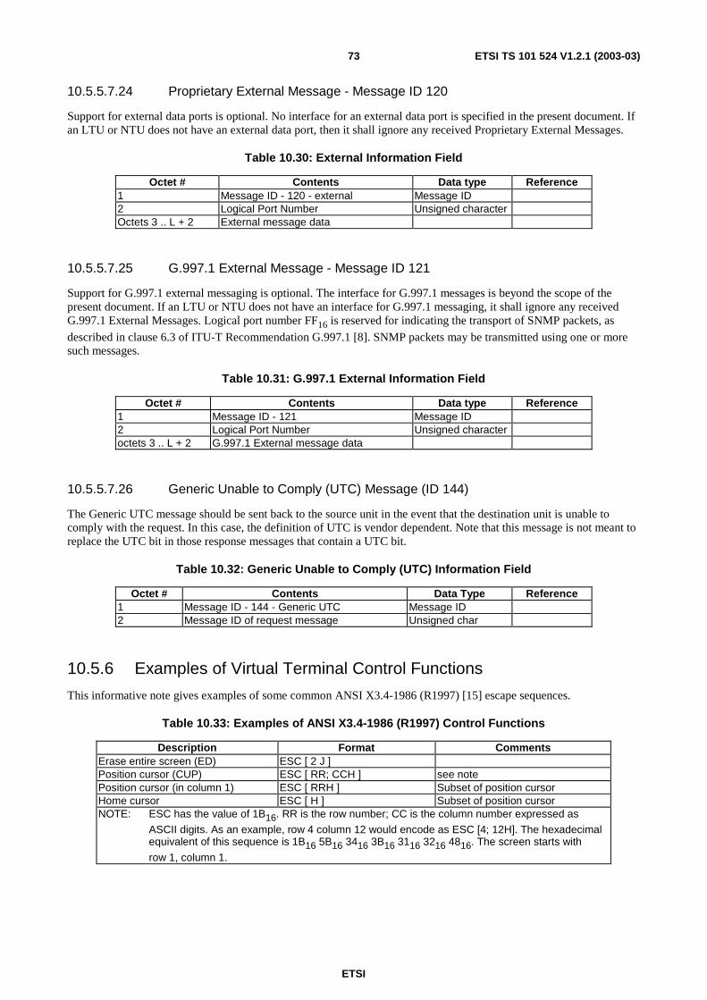
ETSI
ETSI TS 101 524 V1.2.1 (2003-03) 73
10.5.5.7.24 Proprietary External Message - Message ID 120
Support for external data ports is optional. No interface for an external data port is specified in the present document. If an LTU or NTU does not have an external data port, then it shall ignore any received Proprietary External Messages.
Table 10.30: External Information Field
Octet # Contents Data type Reference 1 Message ID - 120 - external Message ID 2 Logical Port Number Unsigned character Octets 3 .. L + 2 External message data
10.5.5.7.25 G.997.1 External Message - Message ID 121
Support for G.997.1 external messaging is optional. The interface for G.997.1 messages is beyond the scope of the present document. If an LTU or NTU does not have an interface for G.997.1 messaging, it shall ignore any received G.997.1 External Messages. Logical port number FF16 is reserved for indicating the transport of SNMP packets, as
described in clause 6.3 of ITU-T Recommendation G.997.1 [8]. SNMP packets may be transmitted using one or more such messages.
Table 10.31: G.997.1 External Information Field
Octet # Contents Data type Reference 1 Message ID - 121 Message ID 2 Logical Port Number Unsigned character octets 3 .. L + 2 G.997.1 External message data
10.5.5.7.26 Generic Unable to Comply (UTC) Message (ID 144)
The Generic UTC message should be sent back to the source unit in the event that the destination unit is unable to comply with the request. In this case, the definition of UTC is vendor dependent. Note that this message is not meant to replace the UTC bit in those response messages that contain a UTC bit.
Table 10.32: Generic Unable to Comply (UTC) Information Field
Octet # Contents Data Type Reference 1 Message ID - 144 - Generic UTC Message ID 2 Message ID of request message Unsigned char
10.5.6 Examples of Virtual Terminal Control Functions
This informative note gives examples of some common ANSI X3.4-1986 (R1997) [15] escape sequences.
Table 10.33: Examples of ANSI X3.4-1986 (R1997) Control Functions
Description Format Comments Erase entire screen (ED) ESC [ 2 J ] Position cursor (CUP) ESC [ RR; CCH ] see note Position cursor (in column 1) ESC [ RRH ] Subset of position cursor Home cursor ESC [ H ] Subset of position cursor NOTE: ESC has the value of 1B16. RR is the row number; CC is the column number expressed as
ASCII digits. As an example, row 4 column 12 would encode as ESC [4; 12H]. The hexadecimal equivalent of this sequence is 1B16 5B16 3416 3B16 3116 3216 4816. The screen starts with
row 1, column 1.

ETSI
ETSI TS 101 524 V1.2.1 (2003-03) 74
11 Electrical characteristics of a SDSL transceiver
11.1 General This clause describes the electrical characteristics of an SDSL transceiver.
The electrical characteristics of an SDSL transceiver shall be such as to enable the performance requirements of appropriate applications, which are described in application dependent annexes, to be met. In addition, the following specific electrical line characteristics are required.
11.2 Transmitter/Receiver impedance and return loss The nominal driving point impedance at the line side of an SDSL transceiver shall be 135 Ω. The minimum return loss with respect to 135 Ω over a frequency band of 1 kHz to 1 MHz shall be:
- 12 dB from 50 kHz to fsym/2 kHz as shown in figure 11.1with a slope of 20 dB/decade below/above, respectively, these frequencies.
20 dB/decade roll-off
Return Loss (dB)
12
0
20 dB/decade roll-off
Frequency 12,56 kHz 50 kHz fsym/2 1,99 × fsym
NOTE: It is expected that the above specification of return loss will be replaced by a specification of another electrical characteristic that is more appropriate and will probably be a frequency dependent output impedance. This enables a prediction of signal levels on real cables from signal level measurements under different impedance conditions.
Figure 11.1: Minimum return loss of a SDSL system
NOTE: The intention of the return loss specification is to maintain some power constraint, even under severe mismatched conditions, when SDSL modems are connected to real cables. A minimum return loss bounds the (complex) output impedance Zs within a restricted range around the design impedance RV = 135 Ω, and thus the maximum available power from that source. Therefore it is expected that the power dissipated into a complex load impedance ZL should never exceed the appropriate PSD masks and
maximum aggregate powers for all values ZL in the range of 10 Ω < |ZL| < 2 000 Ω, as specified for
Rv = 135 Ω in clause 9.4 and tables 9.10 and 9.12. The extension of the existing power constraints to the severely mismatched case is for further study.

ETSI
ETSI TS 101 524 V1.2.1 (2003-03) 75
11.3 Unbalance about earth
11.3.1 Longitudinal conversion loss
The longitudinal conversion loss is given by:
- LCL = 20 log (el/em) [dB];
where el is the applied longitudinal voltage referenced to the building ground and em is the resultant metallic voltage
appearing across a 135 Ω termination.
The longitudinal conversion loss of the system shall meet the requirement of: 40 dB between 5 kHz and fBaud/2 kHz as shown in figure 11.2, with a slope of 20 dB/decade below respectively above these frequencies. This requirement ensures that the overall LCL is not significantly worse than that of the DLLs alone.
20 dB/decaderoll-off
LongitudinalBalance
(dB)
40
20 dB/decaderoll-off
Frequency
5 kHz fsym/2
Figure 11.2: Minimum longitudinal conversion loss for a SDSL system
Figure 11.3 defines a measurement method for longitudinal conversion loss. For direct use of this configuration, measurement should be performed with the IUT powered up but inactive (no transmitted signal; driving 0 V).
R1
R2
em V
DC
el
Longitudinal signalgenerator
Measuring set(well balanced)
IUT
NOTE 1: * These resistors have to be matched: R1 = R2 = 135/2 Ω and R1/R2 = 1 ± 0,1 %. NOTE 2: ** For LTU test only if remote power feeding is supplied. NOTE 3: *** For NTU test only if remote power feeding is required. NOTE 4: During regenerator test (where required) each wire on the side which is not under test has to be connected
to ground by a terminating impedance having the value of 135/2 Ω in series with a capacitance of 0,33 µF.
Figure 11.3: Measurement method for longitudinal conversion loss

ETSI
ETSI TS 101 524 V1.2.1 (2003-03) 76
11.3.2 Longitudinal output voltage
The longitudinal component of the output signal shall have an rms voltage, in any 4 kHz equivalent bandwidth averaged in any second period, < -50 dBV over the frequency range 100 Hz to 400 kHz. Compliance with this limitation is required with a longitudinal termination having an impedance of 100 Ω in series with 0,15 µF nominal. Note that the EMC requirements of clause 14.4 must also be met.
Figure 11.4 defines a measurement method for longitudinal output voltage. For direct use of this test configuration, the IUT should be able to generate a signal in the absence of a signal from the far end. The ground reference for these measurements shall be the building ground.
IUT
R1
R2
V DC
Spectrum analyser
150 nF
100 Ω
NOTE 1: *These resistors have to be matched: R1 = R2 = 135/2 Ω and R1/R2 = 1 ± 0,1 %. NOTE 2: **For LTU test only if remote power feeding is supplied. NOTE 3: ***For NTU test only if remote power feeding is required. NOTE 4: During regenerator test (where required) each wire on the side which is not under test has to be connected
to ground by a terminating impedance having the value of 135/2 Ω in series with a capacitance of 0,33 µF.
Figure 11.4: Measurement method for longitudinal output voltage
11.4 Signal transfer delay The SDSL-core as specified in clause 4 Reference configuration shall be capable of providing one-way, single-span latency of ≤ 500 µs for user data rates ≥ 1,5 Mbit/s and ≤ 1,25 ms for user data rates < 1,5 Mbit/s.
However, for non-packet based services the one-way signal transfer delay between the application interfaces at the customer and the network side calculated as the mean value of both directions shall be ≤ 1,25 ms.
12 Laboratory performance measurements
12.1 General The purpose of transmission performance tests is to stress SDSL transceivers in a way that is representative of a high system penetration scenario in operational access networks. This high penetration approach enables operators to define deployment rules that apply to most operational situations. It also means that, in individual operational cases, characterized by lower noise levels and/or insertion loss values, the SDSL system under test may perform better than tested.

ETSI
ETSI TS 101 524 V1.2.1 (2003-03) 77
The performance requirements given in this clause are dedicated to SDSL transceivers, but the concept is applicable to other systems such as "ADSL over ISDN". The design impedance RV is 135 Ω. All spectra are representing single sided Power Spectral Densities (PSD).
12.2 Test procedure The purpose of this clause is to provide an unambiguous specification of the test set-up, the insertion path and the way signal and noise levels are defined. The tests are focused on the noise margin, with respect to the crosstalk noise or impulse noise levels when SDSL signals under test are attenuated by standard test-loops and interfered with standard crosstalk noise or impulse noise. This noise margin indicates what increase of crosstalk noise or impulse noise level is allowed under (country-specific) operational conditions to ensure sufficient transmission quality.
Note that the combination of all tolerances in test equipment (impairment generator, cable simulator, etc.) leaves an inaccuracy/uncertainty on the noise margin measurements of the order of 1,25 dB. Techniques addressing this accuracy are under study.
12.2.1 Test set-up definition
Figure 12.1 illustrates the functional description of the test set-up. It includes:
- a Bit Error Ratio Test Set (BERTS) that applies a 215 - 1 Pseudo Random Bit Sequence (PRBS) test signal to the transmitter in the direction under test at the bit rate required. The transmitter in the opposite direction shall be fed with a similar PRBS signal, although the reconstructed signal in this path need not be monitored;
- the testloops, as specified in clause 12.4;
- an adding element to add the (common mode and differential mode) impairment noise (a mix of random, impulsive and harmonic noise), as specified in clause 12.5;
- an impairment generator, as specified in clause 12.5, to generate both the differential mode and common mode impairment noise, that are fed to the adding element;
- a high impedance, and well-balanced differential voltage probe (e.g. better than 60 dB across the whole band of the SDSL system under test) connected with level detectors such as a spectrum analyser or a true rms voltmeter;
- a high impedance, and well-balanced common mode voltage probe (e.g. better than 60 dB across the whole band of the SDSL system under test) connected with level detectors such as a spectrum analyser or a true rms voltmeter.
addingelement
test "cable"
test loop
impairmentgenerator
[A1]
[B1]
Txmodem
under test
PRBSpattern
generator
applicationinterface
Rxmodem
under testBERTSreceiver
applicationinterface
GND
probevoltage
differentialprobe
voltage
U1
GND
[A2]
[B2]
probevoltage
U2
leveldetector
leveldetector
leveldetector
NOTE: To allow test reproducibility, the testing equipment and the Termination Units (LTU and NTU) should refer to an artificial earth. If the Termination Units have no earth terminal, the test should be performed while the Termination Units are placed on a metal plate (of sufficient large size) connected to earth.
Figure 12.1: Functional description of the set-up of the performance tests
NOTE: The functional description of injecting ingress noise is not complete and requires further study.

ETSI
ETSI TS 101 524 V1.2.1 (2003-03) 78
The two-port characteristics (transfer function, impedance) of the test-loop, as specified in clause 12.4, are defined between port Tx (node pairs A1, B1) and port Rx (node pair A2, B2). The consequence is that the two-port characteristics of the test "cable" in figure 12.1 must be properly adjusted to take full account of non-zero insertion loss and non-infinite shunt impedance of the adding element and impairment generator. This is to ensure that the insertion of the generated impairment signals does not appreciably loads the line.
The balance about earth, observed at port Tx, at port Rx and at the tips of the voltage probe shall exhibit a value that is 10 dB greater than the transceiver under test. This is to ensure that the impairment generator and monitor function do not appreciably deteriorate the balance about earth of the transceiver under test.
The signal flow through the test set-up is from port Tx to port Rx, which means that measuring upstream and downstream performance requires an interchange of transceiver position and test "cable" ends.
The received signal level at port Rx is the level, measured between node A2 and B2, when port Tx as well as port Rx are terminated with the SDSL transceivers under test. The impairment generator is switched off during this measurement.
Testloop #1, as specified in clause 12.4.2, shall always be used for calibrating and verifying the correct settings of generators G1-G7, as specified in clause 12.5, when performing performance tests.
The transmitted signal level at port Tx is the level, measured between node A1 and B1, under the same conditions.
The impairment noise shall be a mix of random, impulsive and harmonic noise, as defined in clause 12.5. The level that is specified in clause 12.5 is the level at port Rx, measured between node A2 and B2, (and includes both differential mode and common mode impairments) while port Tx as well as port Rx are terminated with the design impedance RV. These impedances shall be passive when the transceiver impedance, in the switched-off mode, is different from this value.
12.2.2 Signal and noise level definitions
The signal and noise levels are probed with a well-balanced differential voltage probe, and the differential impedance between the tips of the probe shall be higher than the shunt impedance of 100 kΩ in parallel with 10 pF. Figure 12.1 shows the probe position when measuring the Rx signal level at the LT or NT receiver. Measuring the Tx signal level requires the connection of the tips to node pair [A1, B1].
The various PSDs of signals and noises specified in the present document are defined at the Tx or Rx side of the set-up. The levels are defined when the set-up is terminated, as described above, with the design impedance RV or with SDSL transceivers under test.
Probing an rms-voltage Urms [V] in this set-up, over the full signal band, means a power level of P [dBm] that equals:
P = 10 × log10 ( Urms2/RV × 1 000) [dBm]
Probing an rms-voltage Urms [V] in this set-up, within a small frequency band of ∆f [Hz], corresponds to an average spectral density level of P [dBm/Hz] within that filtered band that equals:
P = 10 × log10 (Urms2/RV × 1 000/∆f) [dBm/Hz]
The bandwidth ∆f identifies the noise bandwidth of the filter, and not the -3 dB bandwidth.
12.2.3 Noise injection network
12.2.3.1 Differential mode injection
The noise injector for differential mode noise is a two-port network in nature, and may have additional ports connected to the impairment generator. The Norton equivalent circuit diagram is shown in figure 12.2. The current source Ix is
controlled by the impairment generator. The parasitic shunt impedance Zinj shall have a value of |Zinj| > 4 kΩ in the frequency range from 100 Hz to 2 MHz.

ETSI
ETSI TS 101 524 V1.2.1 (2003-03) 79
I xZinjR -portxL -portx
Figure 12.2: Norton equivalent circuit diagram for the differential mode noise injection
12.2.3.2 Common mode injection
The specification of this injection network is for further study.
12.2.4 Noise levels calibration
12.2.4.1 Differential mode noise calibration
The differential mode noise injection is calibrated using the configuration shown in figure 12.3. During calibration the Rx side of the noise injector is terminated by the design impedance RV (= 135 Ω) and the LX side of the noise injector is
terminated by an impedance ZLx. The noise levels given in clause 12.5 specify the PSD dissipated in RV on the RX side
when ZLx on the Lx side is equal to the calibration impedance Zcal. The impedance Zcal is defined in figure 12.4.
Rv
Ux
impairmentgenerator
differential mode
noise injection
networkZLx
R -portxL -portx
Figure 12.3: Configuration for noise level calibration
150nF
150 ohm
47nF
750 ohm120 ohm
Figure 12.4: Calibration impedance Zcal
The impedance ZLx on the Lx side of the noise injection circuit is equal to the calibration impedance Zcal as given in
figure 12.4. The PSD dissipated in the impedance Rv shall be equal to the noise PSD Pxn(f) defined in clause 12.5.1.
NOTE: This is theoretically equivalent to the following: for an arbitrary value of the impedance ZLx, the PSD
dissipated in Rv is equal to:
( ) ( )fPZfGfP xnLxcal ),(= .
The impedance dependent correction factor is specified as:
2
111
111
),(vinjcal
vinjLx
RZZ
RZZ
LxZfG++
++= ,
where Zcal is the calibration impedance given in figure 12.4, Zinj is the Norton equivalent impedance of the noise
injection circuit (see figure 12.2), and Rv = 135 Ω is the SDSL design impedance.

ETSI
ETSI TS 101 524 V1.2.1 (2003-03) 80
The noise generator gain settings determined during calibration shall be used during performance testing. During performance testing the noise injection circuit will be configured as shown in figure 12.1. Because the loop impedance and the impedance of the modem under test may differ from the impedance's ZLx and Rv used during calibration, the
voltage over the Rx port of the modem may differ from the voltage Ux observed during calibration.
12.2.4.2 Common mode noise calibration
This calibration method is for further study.
12.3 Performance test procedure The test performance of the SDSL transceiver shall be such that the Bit Error Ratio (BER) on the disturbed system is less than 10-7, while transmitting a pseudo random bit sequence. The BER should be measured after at least 109 bits have been transmitted.
The tests are carried out with a margin which indicates what increase of noise is allowed to ensure sufficient transmission quality. Network operators may calculate their own margins for planning purposes based on a knowledge of the relationship between the present document test set and their network characteristics.
A test sequence as specified in table 12.1 shall be conducted. The testloops are specified in figure 12.5. They are characterized by the insertion loss Y, which depends on the data rate to be transported and has to be scaled adequately.
In table 12.1, upstream and downstream only determine the topology of the test loop. The LTU must pass all test 1 through 12. The NTU must pass all tests 1 through 12.
A test is defined as the measurement of a given BER associated with a single test path, direction, test noise, rate and margin. The ensemble of tests associated with a particular value of N in table 12.1 is defined as a test set.

ETSI
ETSI TS 101 524 V1.2.1 (2003-03) 81
Table 12.1: Test sequence for performance testing
N Test Path Direction (see note 6)
Comments
1 #1 (see note 1) Upstream Y = 0 dB; Test noise A (see notes 5 and 7) 2 #2 Upstream Y = Y1 (see note 2); Test noise A, C, and D (see notes 7 and 8) 3 #3 Upstream Y = Y1; Test noise D (see notes 5, 7 and 8) 4 #4 Downstream Y = Y1; Test noise A and C (see notes 5 and 7) 5 #5 Upstream Y = Y1; Test noise B (see notes 5 and 7) 6 #6 Downstream Y = Y1; Test noise A and C (see notes 5 and 7) 7 #7 Downstream Y = Y1; Test noise A, B, C, and D (see notes 5 and 7) 8 Common mode rejection test (see note 4) 9 (see note 3) (see note 3) Y = Y2; Test noise is the noise corresponding to the test with the highest BER in
test sets 1 through 7 (see note 7) 10 (see note 3) (see note 3) Y = Y3 ; No added impairment; BER < 10-8 11 #2 Upstream Y = Y1 ; Impulse test as described in <TBD> 12 As <TBD> <TBD> Micro interruption test as described in <TBD> NOTE 1: Test Path = #1 means that the path under test shall be connected with testloop #1 as defined in figure 12.5. NOTE 2: Y1 = Y dB (as specified in table 10.3 for noise models B, C and D and in table 10.2 for noise model A),
Y2 = Y1 - 10 dB, Y3 = Y1 + 3 dB. NOTE 3: The tests (for any data rate) are carried out on the loop that gives the highest BER [for that data rate] in test
sets 1 though 7, when the test noise is increased by 6 dB. If no errors in 109 bits are recorded for all the tests in test sets 1 through 7, then loop #3 upstream is used for this test set by default.
NOTE 4: The measuring arrangement for this test is specified in ITU-T Recommendation O.9 [12]. NOTE 5: Only tested for lowest and highest data rate in tables 12.2 and 12.3 that the equipment supports and for
asymmetric PSDs when supported. NOTE 6: Upstream means that the unit under test is connected to the LT end of the testloop and downstream means
that the unit under test is connected to the NT end of the testloop. For example, test set 5 for an LTU would connect the LTU under test to the LT end of the loop as shown in figure 12.5 and apply noise model B.LT to the LT end. The same test for an NTU would connect the NTU under test to the LT end of the loop as shown in figure 12.5 and apply noise model B.NT to the LT end.
NOTE 7: The BER shall be less than 10-7 when the test noise is increased by 6 dB (this is equivalent to 6 dB of margin. NOTE 8: In order to reduce the number of noise shapes used, a mandatory noise shape substitution rule is given in
clause 12.5.4.3. NOTE 9: To test the 4-wire mode, while one path is under test, the second path must be connected to a loop. The
characteristics of the second loop must not be worse than the ones of the path under test. Furthermore, the differential delay between the path under test and the path connected to the second loop should not exceed the value of the differential delay buffer specified in clause 7.1.7.
NOTE: Table 12.1 constitutes a rationalized subset of tests that are considered to be representative of the full set of tests. For conformance, these tests (subset) are required. Other tests (possibly based on other testloops) are currently under study with ETSI TM6.
12.4 Testloops
12.4.1 Functional description
The testloops in figure 12.5 are based on the existing HDSL testloops as defined in TS 101 135 [1]. A Technical Specification for unified testloops across all DSL-technologies is currently under development. When the present document becomes available and is judged appropriate for SDSL testing, it will replace the current testloops.
The length of the individual loops are chosen such that the transmission characteristics of all loops are comparable (see figure 12.5). The purpose of this is to stress the equalizer of the SDSL modem under test similarly over all loops, when testing SDSL at a specific bit rate. The total length of each loop is described in terms of physical length, and the length of the individual sections as a fixed fraction of this total. If implementation tolerances of one testloop result in its electrical length being out of specification, then its total physical length shall be scaled accordingly to correct this error. One testloop includes bridged taps to achieve rapid variations in amplitude and phase characteristics of the cable transfer function. In some European access networks, these bridge taps have been implemented in the past, which stresses the SDSL modem under test differently. Loop #1 is a symbolic name for a loop with zero (or near zero) length, to prove that the SDSL transceiver under test can handle the potentially high signal levels when two transceivers are directly connected.

ETSI
ETSI TS 101 524 V1.2.1 (2003-03) 82
12.4.2 Testloop topology
The topology of the testloops is specified in figure 12.5. The basic test cable characteristics are shown in annex F.
0 dB Loop #1
(~0,25 × Y dB) (~0,25 × Y dB) (~0,25 × Y dB) (~0,25 × Y dB) Loop #3
120 Ω
(PE04)
0,1834×L3 0,2866×L3 0,1834×L3 0,3466×L3
(Y dB) Loop #2
120 Ω
(PE04)
L2
(~0,25 × Y dB) (~0,25 × Y dB) (~0,50 × Y dB) Loop #4
159 Ω (PE05)
106 Ω (PE06)
120 Ω (PE04)
0,2866×L4 0,3668×L4 0,3466×L4
(~0,80 × Y dB) 100 m 100 m
Loop #5 73 Ω (PVC04)
73 Ω (PVC04)
L5 - 200m (~0,10 × Y) (~0,10 × Y)
50 m 300 m (~0,60 × Y dB) (~0,2 × Y dB)
Loop #7 120 Ω
(PE04)
75 Ω
(PVC032) 67 Ω
(PVC063)
159 Ω
(PE05)
0,6135×(L7-350m) 0,3865×(L7-350m)
(~0,60 × Y dB) (~0,20 × Y)
500 m 500 m
Loop #6
120 Ω
(PE04)
120 Ω (PE04)
(PE04) (PE04)
0,7143×L6 0,2857×L6
NTU-Side (Central office) LTU-Side
(Customer premises) downstream direction
upstream direction
106 Ω (PE06)
159 Ω (PE05)
120 Ω (PE04)
124 Ω (PE08)
NOTE 1: The values for Y and L are to be found in tables 12.2 and 12.3. NOTE 2: Due to mismatches and Bridged Taps, the total attenuation of the testloops differs from the sum of the
attenuation of the parts. NOTE 3: The impedances are for information only. They refer to the characteristic impedances of the test cables
measured at 300 kHz.
Figure 12.5: Testloop topology

ETSI
ETSI TS 101 524 V1.2.1 (2003-03) 83
12.4.3 Testloop length
The length of each testloop for SDSL transmission systems is specified in tables 12.2 and 12.3. The specified insertion loss Y at the specified test frequency measured with a 135 Ω termination (electrical length) is mandatory. If implementation tolerances of one testloop result in its electrical length being out of specification, then its total physical length shall be scaled accordingly to adjust this error.
The test frequency fT is chosen to be a typical mid-band frequency in the spectrum of long range SDSL systems. The
length is chosen to be a typical maximum value that can be handled correctly by the SDSL transceiver under test. This value is bit rate dependent; the higher the payload bit rate, the lower is the insertion loss that can be handled in practice.
Table 12.2: Values of the electrical length Y of the SDSL noise testloops, when testing SDSL at noise model A
Payload Bit rate [kb/s]
fT [kHz]
Y [dB] @fT,
@135 ΩΩΩΩ
L1 [m]
L2 [m]
L3 [m]
L4 [m]
L5 [m]
L7 [m]
fT [kHz]
Y [dB] @fT,
@135 ΩΩΩΩ
L6 [m]
384 150 43,0 < 3 4 106 5 563 5 568 11 064 4 698 115 40,5 3 165 512 150 37,0 < 3 3 535 4 787 4 789 9 387 3 996 115 35,0 2 646 768 150 29,0 < 3 2 773 3 747 3 753 7 153 3 062 275 34,5 1 904 1 024 150 25,5 < 3 2 439 3 285 3 291 6 174 2 668 275 30,0 1 547 1 280 150 22,0 < 3 2 105 2 829 2 837 5 193 2 266 275 26,0 1 284 1 536 150 19,0 < 3 1 820 2 453 2 455 4 357 1 900 250 21,5 1 052 2 048 (s) 200 17,5 < 3 1 558 2 046 2 052 3 285 1 550 250 18,5 748 2 304 (s) 200 15,5 < 3 1 381 1 815 1 820 2 789 1 331 250 16,5 583 2 048 (a) 250 21,0 < 3 1 743 2 264 2 272 3 618 1 726 250 21,0 1 001 2 304 (a) 250 18,0 < 3 1 494 1 927 1 937 2 915 1 402 250 18,0 702 NOTE: The electrical length Y (insertion loss at specified frequency fT) is mandatory, the
(estimated) physical lengths L1-L7 are informative. (s) those electrical lengths apply to the symmetric PSD. (a) those electrical lengths apply to the asymmetric PSD.
Table 12.3: Values of the electrical length Y of the SDSL noise testloops, when testing SDSL at noise model B, C or D
Payload Bit rate [kb/s]
fT [kHz]
Y [dB] @fT,
@135 ΩΩΩΩ
L1 [m]
L2 [m]
L3 [m]
L4 [m]
L5 [m]
L7 [m]
fT [kHz]
Y [dB] @fT,
@135 ΩΩΩΩ
L6 [m]
384 150 50,0 < 3 4 773 6 471 6 477 13 021 5 508 115 47,5 3 859 512 150 44,0 < 3 4 202 5 692 5 698 11 344 4 814 115 41,5 3 261 768 150 35,5 < 3 3 392 4 592 4 596 8 970 3 815 275 42,0 2 536 1 024 150 32,0 < 3 3 058 4 135 4 141 7 990 3 403 275 38,0 2 223 1 280 150 28,5 < 3 2 725 3 678 3 684 7 011 3 006 275 33,5 1 816 1 536 150 25,5 < 3 2 439 3 285 3 291 6 174 2 673 250 29,0 1 680 2 048 (s) 200 24,0 < 3 2 135 2 812 2 820 4 886 2 271 250 25,5 1 426 2 304 (s) 200 21,5 < 3 1 913 2 509 2 518 4 257 2 010 250 23,0 1 208 2 048 (a) 250 28,0 < 3 2 323 3 030 3 034 5 189 2 389 250 28,0 1 607 2 304 (a) 250 25,0 < 3 2 075 2 699 2 705 4 514 2 102 250 25,0 1 387 NOTE: The electrical length Y (insertion loss at specified frequency fT) is mandatory, the
(estimated) physical lengths L1-L7 are informative. (s) those electrical lengths apply to the symmetric PSD. (a) those electrical lengths apply to the asymmetric PSD.

ETSI
ETSI TS 101 524 V1.2.1 (2003-03) 84
12.5 Impairment generator The noise injected by the impairment generator into the test set-up is frequency and testloop length dependent. The noise is also different for downstream performance tests and upstream performance tests. Figure 12.6 illustrates this for the alien noise (other than the SDSL modem under test) when the length of testloop #2 is fixed at 3 km. Figure 12.7 illustrates this for various loop lengths in the case that the alien noise of model "B" is applied. These figures show the alien noise only. The self noise (of SDSL) shall be combined with this alien noise.
0 200 400 600 800 1 MHz -130
-120
-110
-100
-90
-80
-70 Alien noise [model A,B,C] to be injected at LT side, @3 km
0 200 400 600 800 1 MHz -130
-120
-110
-100
-90
-80
-70 Alien noise [model A,B,C] to be injected at NT side, @3 km
dBm/Hz dBm/Hz
A
B C
A
B
C
NOTE: This is the noise, resulting from three of the four noise models for SDSL, in the case that the length of testloop #2 is fixed at 3 km.
Figure 12.6: Examples of alien noise spectra that are to be injected
into the test set-up, while testing SDSL systems
0 200 400 600 800 1 MHz-130
-120
-110
-100
-90
-80
-70Alien noise [B] to be injected at LT side, @[1,2,3,4] km
dBm/Hz
0 200 400 600 800 1 MHz-130
-120
-110
-100
-90
-80
-70Alien noise [B] to be injected at NT side, @[1,2,3,4] km
dBm/Hz
1 km
2 km
3 km
4 km
NOTE: This is the alien noise, resulting from noise model B for SDSL, in the case that the length of testloop #2 varies from 1 km to 4 km. This demonstrates that the test noise is length dependent, to represent the FEXT in real access network cables.
Figure 12.7: Examples of alien noise spectra that are to be injected
into the test set-up, while testing SDSL systems
The definition of the impairment noise for SDSL performance tests is very complex and for the purposes of the present document has been broken down into smaller, more easily specified components. These separate, and uncorrelated, impairment "generators" may therefore be isolated and summed to form the impairment generator for the SDSL system under test. The detailed specifications for the components of the noise model(s) are given in this clause, together with a brief explanation.

ETSI
ETSI TS 101 524 V1.2.1 (2003-03) 85
12.5.1 Functional description
Figure 12.8 defines a functional diagram of the composite impairment noise. It defines a functional description of the combined impairment noise, as it must be probed at the receiver input of the SDSL transceiver under test. The probing is described in clause 12.2.2.
The functional diagram has the following elements:
- the seven impairment "generators" G1 to G7 generate noise as defined in clauses 12.5.3.1 to 12.5.3.7. Their noise characteristics are independent from the testloops and bit rates;
- the transfer function H1(f, L) models the length and frequency dependency of the NEXT impairment, as
specified in clause 12.5.3.1. The transfer function changes with the electrical length of the testloop and with the frequency f, roughly according to f0,75;
- the transfer function H2(f, L) models the length and frequency dependency of the FEXT impairment, as
specified in clause 12.5.3.2. The transfer function changes with the electrical length of the testloop and with the frequency f, roughly according to f times the cable transfer function;
- switches S1-S7 determine whether or not a specific impairment generator contributes to the total impairment during a test;
- amplifier A1 models the property to increase the level of some generators simultaneously to perform the noise margin tests. A value of x dB means a frequency independent increase of the level by x dB over the full band of the SDSL system under test, from fL to fH. Unless otherwise specified, its gain is fixed at 0 dB.
In a practical implementation of the test set-up, there is no need to give access to any of the internal signals of the diagram in figure 12.8. These functional blocks may be incorporated with the testloop and the adding element as one integrated construction.
independent noise generators crossta lk
transfer functions
NEXT noise
FEXT noise
Background noise Cable independent
W hite noise Cable independent
Cable independent Fixed powers, fixed freq
Broadcast RF noise
Cable independent Fixed power, v ariable freq
Am ateur RF noise
Im pulsive noise
bursty in nature Cable independent
G 1
G 2
G 3
G 4
G 5
G 6
G 7
S1
S2
S3
S4
ΣΣΣΣ A1 H 2 (f,L)
H 1 (f,L)
S5d
S6d
S7
S5c
S6c
ΣΣΣΣ
Probe level
ΣΣΣΣ
differential m ode
com m on m ode
Probe level
Figure 12.8: Functional diagram of the composition of the impairment noise
NOTE 1: Generator G7 is the only one, which is symbolically shown in the time domain.
NOTE 2: The precise definition of impulse noise margin is for further study.

ETSI
ETSI TS 101 524 V1.2.1 (2003-03) 86
The functional diagram (see figure 12.8) will be used for impairment tests in downstream and upstream direction. Several scenarios have been identified to be applied to SDSL testing. These scenarios are intended to be representative of the impairments found in metallic access networks.
Each scenario (or noise model) results in a length-dependent and test loop-dependent PSD description of noise. Each noise model is subdivided into two parts: one to be injected at the LT-side, and another to be injected at the NT-side of the SDSL modem link under test. Therefore, seven individual impairment generators G1 to G7 can represent different values for each noise model they are used in. Specifically, G1 and G2 are dependent on which unit, LT or NT, is under test.
Generators G1-G4 represent cross talk noise. The spectral power Pxn(f) for cross talk noise is characterized by the sum:
Pxn(f) = |A1|2 × |H1(f,L)|2 × PG1(f) + |H2(f,L)|2 × PG2(f) + PG3(f) + PG4(f)
Each component of this sum is specified in the following clauses. Only the noise generators that are active during testing should be included during calibration. This combined impairment noise is applied to the receiver under test, at either the LT (for upstream) or NT (for downstream) ends of the test-loop.
Generators G5 and G6 represent ingress noise.
12.5.2 Cable crosstalk models
The purpose of the cable cross-talk models is to model both the length and frequency dependency of crosstalk measured in real cables. These crosstalk transfer functions adjust the level of the noise generators in figure 12.8 when the electrical length of the testloops is changed. The frequency and length dependency of these functions is in accordance with observations from real cables. The specification is based on the following constants, parameters and functions:
- variable f identifies the frequency in Hz;
- constant f0 identifies a chosen reference frequency, which was set to 1 MHz;
- variable L identifies the physical length of the actual testloop in meters. This physical length is derived from the specified electrical length using the cable models in annex G and the cable characteristics of annex F. Values are summarized in tables 12.2 and 12.3 for each combination of payload bit rate, noise model and testloop;
- constant L0 identifies a chosen reference length, which was set to 1 km;
- transfer function sT0(f, L) represents the frequency and length dependent amplitude of the transfer function of
the actual testloop. This value equals sT0 = |s21|, where s21 is the transmission s-parameter of the loop
normalized to 135 Ω. Annex G provides formulas to calculate this s-parameter;
- constant Kxn identifies an empirically obtained number that scales the NEXT transfer function H1(f, L). The
resulting transfer function represents a power summed crosstalk model of the NEXT as it was observed in a test cable. Although several disturbers and wire pairs were used, this function H1(f, L) is scaled down as if it
originates from a single disturber in a single wire pair;
- constant Kxf identifies an empirically obtained number that scales the FEXT transfer function H2(f, L). The
resulting transfer function represents a power summed crosstalk model of the FEXT as it was observed in a test cable. Although several disturbers and wire pairs were used, this function H2(f, L) is scaled down as if it
originates from a single disturber in a single wire pair.
The transfer functions in table 12.4 shall be used as crosstalk transfer functions in the impairment generator.

ETSI
ETSI TS 101 524 V1.2.1 (2003-03) 87
Table 12.4: Definition of the crosstalk transfer functions
H1(f, L) = Kxn × (f/f0)0,75 × 1 – |sT0(f, L)|4
H2(f, L) = Kxf × (f/f0) × (L/L0) × |sT0(f, L)|
Kxn = 10(-50/20) ≈ 0,0032, f0 = 1 MHz
Kxf = 10(-45/20) ≈ 0,0056, L0 = 1 km
sT0(f, L) = testloop transfer function
NOTE: These values are rounded values, and chosen to be close to the ANSI T1E1.4 VDSL draft system requirements. This choice is equivalent to 50 dB NEXT loss and 45 dB EL-FEXT loss at a cable section of 1 km. At this moment, it is by no means sure that these are reasonable values to represent the "average" European cables. The few measurements that are available for European cables demonstrate sometimes significant differences from the above values. This is an area of further study.
12.5.3 Individual impairment generators
12.5.3.1 Equivalent NEXT disturbance generator [G1.xx]
The NEXT noise generator represents the equivalent disturbance of all impairment that is identified as crosstalk noise from a predominantly near end origin. This noise, filtered by the NEXT crosstalk coupling function of clause 12.5.2, will represent the contribution of all NEXT to the composite impairment noise of the test.
The PSD of this noise generator is one of the PSD profiles, as specified in clause 12.5.4. For testing upstream and downstream performance different PSD profiles shall be used, as specified below:
- G1.UP.# = X.LT.# = (XS.LT.# ♦ XA.LT.#)
- G1.DN.# = X.NT.# = (XS.NT.# ♦ XA.NT.#)
The symbols in this expression, refer to the following:
- Symbol "#" is a placeholder for noise model "A", "B" , "C" or "D".
- Symbol "X.LT.#" and "X.NT.#" refers to the overall crosstalk profile, as defined in clause 12.5.4.1.
- Symbol "XS.LT.#" and "XS.NT.#" refers to the self crosstalk profile, as defined in clause 12.5.4.1.1.
- Symbol "XA.LT.#" and "XA.NT.#" refers to the alien crosstalk profile, as defined in clause 12.5.4.1.2.
- Symbol "♦ " refers to the FSAN crosstalk sum of two PSDs. This FSAN crosstalk sum is defined as PX = (PXS
Kn + PXAKn)1/Kn, where P denotes the PSDs in W/Hz, and Kn = 1/0,6.
In the case that the overall crosstalk noise is defined as the combination of self-crosstalk and alien crosstalk, a weighed sum "♦ " of two individually defined profiles has to be evaluated.
The NEXT transfer function H1(f,L) is modelled separately in clause 12.5.2.
The noise of this noise generator shall be uncorrelated with all the other noise sources in the impairment generator, and uncorrelated with the SDSL system under test. The noise shall be random in nature and near Gaussian distributed, as specified in clause 12.5.4.2.

ETSI
ETSI TS 101 524 V1.2.1 (2003-03) 88
12.5.3.2 Equivalent FEXT disturbance generator [G2.xx]
The FEXT noise generator represents the equivalent disturbance of all impairment that is identified as crosstalk noise from a predominantly Far End origin. This noise, filtered by the FEXT crosstalk coupling function of clause 12.5.2, will represent the contribution of all FEXT to the composite impairment noise of the test.
The PSD of this noise generator is one of the PSD profiles, as specified in clause 12.5.4. For testing upstream and downstream performance different PSD profiles shall be used, as specified below:
- G2.UP.# = X.NT.# = (XS.NT.# ♦ XA.NT.#)
- G2.DN.# = X.LT.# = (XS.LT.# ♦ XA.LT.#)
The symbols in this expression, refer to the following:
- Symbol "#" is a placeholder for noise model "A", "B", "C" or "D".
- Symbol "X.LT.#" and "X.NT.#" refers to the overall crosstalk profiles, as defined in clause 12.5.4.1.
- Symbol "XS.LT.#" and "XS.NT.#" refers to the self crosstalk profiles, as defined in clause 12.5.4.1.1.
- Symbol "XA.LT.#" and "XA.NT.#" refers to the alien crosstalk profiles, as defined in clause 12.5.4.1.2.
- Symbol "♦ " refers to the FSAN crosstalk sum of two PSDs. This FSAN crosstalk sum is defined as PX = (PXS
Kn + PXAKn)1/Kn, where P denotes the PSDs in W/Hz, and Kn = 1/0,6.
In the case that the overall crosstalk noise is defined as the combination of self crosstalk and alien crosstalk, a weighed sum "♦ " of two individually defined profiles has to be evaluated.
The FEXT transfer function H2(f,L) is modelled separately in clause 12.5.2.
The noise of this noise generator shall be uncorrelated with all the other noise sources in the impairment generator, and uncorrelated with the SDSL system under test. The noise shall be random in nature and near Gaussian distributed, as specified in clause 12.5.4.2.
12.5.3.3 Background noise generator [G3]
The background noise generator is inactive and set to zero.
12.5.3.4 White noise generator [G4]
The white noise generator has a fixed, frequency independent value, and is set to a level between –140 dBm/Hz and –120 dBm/Hz, into 135 Ω. The noise of this noise generator shall be uncorrelated with all the other noise sources in the impairment generator, and uncorrelated with the SDSL system under test. The noise shall be random in nature and near Gaussian distributed, as specified in clause 12.5.4.2.
12.5.3.5 Broadcast RF noise generator [G5]
NOTE 1: Work on a specification dealing with generic RFI testing methods is ongoing. It is expected that the specification will contain a complete RFI testing specification, which will be mandatory for SDSL. This is why this clause is currently for information only.
The broadcast RF noise generator represents the discrete-tone line interference caused by amplitude modulated broadcast transmissions in the SW, MW and LW bands, which ingress into the cable. These interference sources have more temporal stability than the amateur (ham) interference (see clause 12.5.3.6) because their carriers are not suppressed. Ingress causes differential mode as well as common mode interference.
The ingress noise signal for differential mode impairment (or common mode impairment) is a superposition of random modulated carriers (AM). The total voltage U(t) of this signal is defined as:
U(t) = ΣΣΣΣk Uk × cos(2π·fk × t + ϕk) × (1 + m × αk(t))

ETSI
ETSI TS 101 524 V1.2.1 (2003-03) 89
The individual components of this ingress noise signal U(t) are defined as follows:
- Uk - The voltage Uk of each individual carrier should be as specified in table 12.5 as power level P (dBm) into
a resistive load R, equal to the design impedance RV = 135 Ω. Note that spectrum analysers will detect levels
that are slightly higher than the values specified in table 12.5 when their resolution bandwidths are set to 10 kHz or more, since they will detect the modulation power as well.
- fk - The frequency fk of each individual carrier should be as specified in table 12.5. The frequency values in
table 12.5 do not represent actual broadcast frequencies but are chosen such that they cover the frequency range that is relevant for SDSL modems. Note that the harmonic relation between the carriers in table 12.5 is minimal.
- ϕϕϕϕk - The phase offset ϕk of each individual carrier shall have a random value that is uncorrelated with the
phase offset of every other carrier in the ingress noise signal.
- m - The modulation depth m of each individually modulated carrier shall be m = 0,32, to enable a modulation index of at least 80 % during the peak levels of the modulation signal m × αk(t).
- ααααk(t) - The normalized modulation noise αk(t) of each individually modulated carrier shall be random in
nature, shall be Gaussian distributed in nature, shall have an RMS value of αrms = 1, shall have a crest factor
of 2,5 or more, and shall be uncorrelated with the modulation noise of each other modulated carrier in the ingress noise signal.
- ∆∆∆∆b - The modulation width ∆b of each modulated carrier shall be at least 2 × 5 kHz. This is equivalent to creating αk (t) from white noise, filtered by a low-pass filter with a cut-off frequency at ∆b/2 = 5 kHz. This
modulation width covers the full modulation band used by AM broadcast stations.
NOTE 2: The precise specification of the spectral shape requirements of the modulation signal is for further study.
The broadcast RF noise generator represents the discrete tone-line interference caused by amplitude modulated broadcast transmissions in the SW, MW and LW bands which ingress into the differential or transmission mode of the wire-pair. These interference sources have more temporal stability than the amateur/ham interference because their carrier is not suppressed. The Modulation Index (MI) is usually up to 80 %. These signals are detectable using a spectrum analyser and result in line spectra of varying amplitude in the frequency band of the SDSL system under test. Maximum observable power levels of up to -40 dBm can occur on telephone lines in the distant vicinity of broadcast AM transmitters. The noise is typically dominated by the closest 10 or so transmitters to the victim wire-pair.
Several noise models are specified in this clause. The average minimum power of each carrier frequency is specified in table 12.5 for each model, but these values are for further study (see the note 1 at the beginning of the clause).
Table 12.5: Average minimum RFI noise power versus frequency
frequency 153 207 270 531 603 711 801 909 981 1 296 kHz power -70 -44 -70 -70 -49 -70 -70 -44 -70 -49 dBm
12.5.3.6 Amateur RF noise generator [G6]
The amateur radio noise generator is identical to the broadcast RF noise generator with different frequency and power values. These values are for further study.
12.5.3.7 Impulse noise generator [G7]
A test with this noise generator is required to prove the burst noise immunity of the SDSL transceiver. This immunity shall be demonstrated on short and long loops and noise to model cross-talk and RFI. The impulsive noise is for further study.

ETSI
ETSI TS 101 524 V1.2.1 (2003-03) 90
12.5.4 Profiles of the individual impairment generators
Crosstalk noise represents all impairment that originates from systems connected to adjacent wire pairs that are bundled in the same cable. Their wires are coupled to the wires of the xDSL system under test, causing this spectrum of crosstalk noise to vary with the electrical length of the testloop.
To simplify matters, the definition of crosstalk noise has been broken down into smaller, more easily specified components. The two generators G1 and G2 represent the "equivalent disturbance". Their noise level originates from a mixture of many disturbers in a real scenario, as if all disturbers are collocated at the ends of the testloops.
This equivalent disturbance, filtered by the NEXT and FEXT coupling functions, will represent the crosstalk noise that is to be injected in the test set-up. This approach has isolated their definition from the NEXT and FEXT coupling functions of the cable.
For SDSL testing, several models for crosstalk noise have been defined. The noise generated by these two equivalent disturbers is specified in this clause in the frequency domain as well as in the time domain.
The frequency domain characteristics of each generator G1 and G2 is defined by a spectral profile, so each noise model has its own pair of spectral profiles:
- the profiles X.LT.# in this clause describe the total equivalent disturbance of a technology mix that is virtually co-located at the LT end of the testloop. This noise is represented by equivalent disturbance generator G1, when stressing upstream signals, and by equivalent disturbance generator G2 when stressing downstream signals;
- the profiles X.NT.# in this clause describe the total equivalent disturbance of a technology mix that is virtually co-located at the NT end of the testloop. This noise is represented by equivalent disturbance generator G2, when stressing upstream signals, and by equivalent disturbance generator G1 when stressing downstream signals.
The PSD levels of equivalent disturbance generator G1 and G2 are interchanged for upstream and downstream testing.
12.5.4.1 Frequency domain profiles for SDSL
This clause specifies the PSD profiles X.LT.# and X.NT.# that apply for the equivalent disturbers G1 and G2 when testing SDSL systems. In this nomenclature "#" is used as a placeholder for noise model "A", "B","C", and "D".
Four noise models have been defined for SDSL:
- type "A" models are intended to represent a high penetration scenario where the SDSL system under test is placed in a distribution cable (up to hundreds of wire pairs) that is filled with many other (potentially incompatible) transmission systems;
- type "B" models are intended to represent a medium penetration scenario where the SDSL system under test is placed in a distribution cable (up to tens of wire pairs) that is filled with many other (potentially incompatible) transmission systems;
- type "C" models are intended to represent a legacy scenario that accounts for systems such as ISDN-PRI (HDB3), in addition to the medium penetration scenario of model "B";
- type "D" models are intended to represent a reference scenario consisting of a cable filled with SDSL systems all operating at the same rate, or filled with SDSL systems operating at different rates.
Noise generator G1 specifies the NEXT component of the noise and is specified in clause 12.5.3.1 for upstream and downstream testing. Noise generator G2 specified the FEXT component of the noise and is specified in clause 12.5.3.2 for upstream and downstream testing.
These profiles shall be met for all frequencies between 1 kHz to 1 MHz.

ETSI
ETSI TS 101 524 V1.2.1 (2003-03) 91
12.5.4.1.1 Self crosstalk profiles
The noise profiles XS.LT.# and XS.NT.#, representing the equivalent disturbance of self crosstalk, are specific to the PSD parameters of the system under test, defined by the specific payload, symmetry and power-back-off features. For compliance with the requirements of the present document, the appropriate nominal PSD from clause 9.4 shall be used.
For testing SDSL, four noise models for self crosstalk have been defined. The LT- and NT-profiles are specified in table 12.6.
In this nomenclature "#" is a placeholder for noise model "A", "B","C" or "D". "SDSL.dn" is the signal spectrum that SDSL transmits in the downstream direction, and "SDSL.up" in the upstream direction.
Table 12.6: Definition of the self crosstalk for SDSL testing
Model A Model B Model C Model D XS.LT.#: "SDSL.dn" + 11,7 dB "SDSL.dn" + 7,1 dB "SDSL.dn" + 7,1 dB "SDSL.dn" + 10,1 dB XS.NT.#: "SDSL.up" + 11,7 dB "SDSL.up" + 7,1 dB "SDSL.up" + 7,1 dB "SDSL.up" + 10,1 dB
NOTE: The different noise models use different gain factors.
12.5.4.1.2 Alien crosstalk profiles
The noise profiles XA.LT.# and XA.NT.#, representing the equivalent disturbance of alien crosstalk. For testing SDSL, four noise models for alien crosstalk have been defined. The LT-profiles are specified in table 12.7 and the NT-profiles in table 12.8. Each PSD profile originates from a mix of disturbers. The alien noise in model D is made inactive, to achieve one pure self crosstalk scenario.
Table 12.7: Break frequencies of the "XA.LT.#" PSD profiles that specify the equivalent disturbance spectra of alien disturbers
XA.LT.A
XA.LT.B
XA.LT.C
XA.LT.D
Freq PSD Freq PSD Freq PSD Freq PSD [Hz] [dBm/Hz] [Hz] [dBm/Hz] [Hz] [dBm/Hz] [Hz] [dBm/Hz]
1 -20,0 1 -25,7 1 -25,7 15 k -20,0 15 k -25,7 15 k -25,7 30 k -21,5 30 k -27,4 30 k -27,4 ALL -∞ 67 k -27,0 45 k -30,3 45 k -30,3
125 k -27,0 70 k -36,3 70 k -36,3 138 k -25,7 127 k -36,3 127 k -36,3 400 k -26,1 138 k -32,1 138 k -32,1
1 104 k -26,1 400 k -32,5 400 k -32,5 2,5 M -66,2 550 k -32,5 550 k -32,5
4,55 M -96,5 610 k -34,8 610 k -34,8 30 M -96,5 700 k -35,4 700 k -35,3
1 104 k -35,4 1 104 k -35,3 4,55 M -103,0 1,85 M -58,5 30 M -103,0 22,4 M -103,0 30 M -103,0
NOTE: The PSD profiles are constructed with straight lines between these break frequencies, when plotted against a logarithmic frequency scale and a linear dBm scale. The levels are defined into a 135 Ω resistive load.

ETSI
ETSI TS 101 524 V1.2.1 (2003-03) 92
Table 12.8: Break frequencies of the "XA.NT.#" PSD profiles that specify the equivalent disturbance spectra of alien disturbers
XA.NT.A
XA.NT.B
XA.NT.C
XA.NT.D
Freq PSD Freq PSD Freq PSD Freq PSD [Hz] [dBm/Hz] [Hz] [dBm/Hz] [Hz] [dBm/Hz] [Hz] [dBm/Hz]
1 -20,0 1 -25,7 1 -25,7 15 k -20,0 15 k -25,7 15 k -25,7 60 k -25,2 30 k -26,8 30 k -26,8 ALL -∞
276 k -25,8 67 k -31,2 67 k -31,2 500 k -51,9 142 k -31,2 142 k -31,2 570 k -69,5 156 k -32,7 156 k -32,7 600 k -69,9 276 k -33,2 276 k -33,2 650 k -62,4 400 k -46,0 335 k -42,0 763 k -62,4 500 k -57,9 450 k -47,9 1,0 M -71,5 570 k -75,7 750 k -45,4
2,75 M -96,5 600 k -76,0 1 040 k -45,5 30 M -96,5 650 k -68,3 2,46 M -63,6
763 k -68,3 23,44 M -103,0 1,0 M -77,5 30 M -103,0 2,8 M -103,0 30 M -103,0
NOTE: The PSD profiles are constructed with straight lines between these break frequencies when plotted against a logarithmic frequency scale and a linear dBm scale. The levels are defined into a 135 Ω resistive load.
12.5.4.2 Time domain profiles of generator G1-G4
The noise, as specified in the frequency domain in clauses 12.5.3.1 to 12.5.3.7, shall be random in nature and near Gaussian distributed. This means that the amplitude distribution function of the combined impairment noise injected at the adding element shall lie between the two boundaries as illustrated in figure 12.9, where the non-shaded area is the allowed region. The boundaries of the mask are specified in table 12.9.
It is expected that noise generators will generate signals that are approximately Gaussian. Therefore, the upper bound of figure 12.9 is loose. PDFs of signals generated by noise generators are expected to be well below the upper bound allowed by the PDF mask shown in figure 12.9.
The amplitude distribution function F(a) of noise u(t) is the fraction of the time that the absolute value of u(t) exceeds the value "a". From this definition, it can be concluded that F(0) = 1 and that F(a) monotonically decreases up to the point where "a" equals the peak value of the signal. From there on, F(a) vanishes:
0)( =aF , for peakua ≥
The boundaries on the amplitude distribution ensure that the noise is characterized by peak values that are occasionally significantly higher than the rms-value of that noise (up to 5 times the rms-value).

ETSI
ETSI TS 101 524 V1.2.1 (2003-03) 93
0 1 2 3 4 5 6 710
-8
10-6
10-4
10-2
100
Flow er
Fupper
a/σ
Mas
k on
F(a
)
Figure 12.9: Mask for the amplitude distribution function
Table 12.9: Upper and lower boundaries of the amplitude distribution function of the noise
Boundary (σσσσ = rms value of noise) interval parameter value Flower(a) = (1 - ε) · 1 - erf((a/σ)/√2) 0 ≤ a/σ < CF crest factor CF = 5
Flower(a) = 0 CF ≤ a/σ < ∞ Gaussian gap ε = 0,1
Fupper(a) = (1 + ε) · 1 - erf((a/σ)/√2) 0 ≤ a/σ < A A = CF/2 = 2,5
Fupper(a) = (1 + ε) · 1 - erf(A/√2) A ≤ a/σ < ∞
The meaning of the parameters in table 12.9 is as follows:
- CF denotes the minimum crest factor of the noise, that characterizes the ratio between the absolute peak value and rms value (CF = |upeak|/urms);
- ε denotes the Gaussian gap that indicates how "close" near Gaussian noise approximates true Gaussian noise;
- A denotes the point beyond which the upper limit is relaxed to allow the use of noise signals of practical repetition length.
12.5.4.3 Mandatory noise shape substitution rule
The strict application of the test procedure requires a different noise shape for each test although some of the noise shapes are very similar. In order to reduce the number of possible noise shapes, the following substitution rule is mandatory. It reduces the number of noise shapes from 280 to 22.
Table 12.10 tabulates the noise substitution rule. The following nomenclature is used to describe a shape:
"Side (C or R) Rate (384 to 2 304) PSDType (s for symmetric) noise model (A to D)"
EXAMPLE 1: C384sA2 represents the noise shape on the LT side for the 384 kbps rate using the symmetric PSD corresponding to noise model A and loop 2.
EXAMPLE 2: C384sAX represents the noise shape on the LT side for the 384 kbps rate using the symmetric PSD corresponding to noise model A and any loop.

ETSI
ETSI TS 101 524 V1.2.1 (2003-03) 94
EXAMPLE 3: Rule 7 requires that the following noise shapes: R384sA1, R384sA2, R384sA3, R384sA4, R384sA5, R384sA6, R384sA7, R512sA1, R512sA2, R512sA3, R512sA4, R512sA5, R512sA6, R512sA7 be replaced by the single noise shape R768sA2.
EXAMPLE 4: Conducting test set 3 of table 12.1 for 384 kbps at the LT end. The loop and transceiver would be set-up as per the test description (loop #3 upstream set to 43 dB @ 150 kHz, which is equivalent to a length of 5 563 m). The transceiver would be set to 384 kbps. The noise shape injected would be "R768sC2" rather than "C384sD3" (rule 9).
Table 12.10: Noise shape substitution rule
Rule # This shape Replaces those shapes (on a row by row basis) where X represents any loop number
1 "C768sA2" "C384sAX" "C512sAX"
2 "C768sC2" "C384sBX" "C512sBX" "C384sCX" "C512sCX"
3 "C1536sA2" "C768sAX" "C1024sAX" "C1280sAX"
4 "C1536sC2" "C768sBX" "C1024sBX" "C1280sBX" "C768sCX" "C1024sCX" "C1280sCX"
5 "C2304sA2" "C1536sAX" "C2048sAX" "C2304sAX" "C1536sAX"
6 "C2304sC2" "C1536sBX" "C2048sBX" "C2304sBX" "C1536sCX" "C2048sCX" "C2304sCX"
7 "R768sA2" "R384sAX" "R512sAX"
8 "R768sB2" "R384sBX" "R512sBX"
9 "R768sC2" "R384sCX" "R512sCX" "C384sDX" "R384sDX" "C512sDX" "R512sDX"
10 "R1536sA2" "R768sAX" "R1024sAX" "R1280sAX" "R1536sAX"
11 "R1536sB2" "R768sBX" "R1024sBX" "R1280sBX" "R1536sBX"
12 "R1536sC2" "R768sCX" "R1024sCX" "R1280sCX" "R1536sCX"
13 "R2048sA2" "R2048sAX"
14 "R2048sB2" "R2048sBX"
15 "R2048sC2" "R2048sCX"
16 "R2304sA2" "R2304sAX"
17 "R2304sB2" "R2304sBX"
18 "R2304sC2" "R2304sCX"
19 "C1280sD2" "C768sDX" "R768sDX" "C1280sDX" "R1280sDX"
20 "C1536sD2" "C1024sDX" "R1024sDX" "C1536sDX" "R1536sDX"
21 "C2048sD2" "C2048sDX" "R2048sDX"
22 "C2304sD2" "C2304sDX" "R2304sD"
12.6 Measurement of noise margin At start-up, the level and shape of crosstalk noise or impulse noise are adjusted, while their level is probed at port Rx to meet the impairment level specification in clause 12.2.2. This relative level is referred to as 0 dB. The transceiver link is subsequently activated, and the bit error ratio of the link is monitored.

ETSI
ETSI TS 101 524 V1.2.1 (2003-03) 95
12.6.1 Measurement of crosstalk noise margin
For measuring the crosstalk margin, the crosstalk noise level of the impairment generator as defined in clause 12.5.4.1, shall be increased by adjusting the gain of amplifier A1 in figure 12.8, equally over the full frequency band of the SDSL system under test, until the bit error ratio is higher than 10-7. This BER will be achieved at an increase of noise of x dB, with a small uncertainty of ∆x dB. This value x is defined as the crosstalk noise margin with respect to a standard noise model.
The noise margins shall be measured using the testloops specified in figure 12.5 and scaled according to tables 12.2 and 12.3.
NOTE: Currently, the injected noise, for the purpose of crosstalk noise margin measurement, consist in the sum of generators G1, G2 and G4 as described in clause 12.5.1. Annex I tabulates the values of the injected noise corresponding to 0 dB margin and a white noise generator value of –140 dBm/Hz. The injected noise should be measured per clause 12.2.3.1. The mandatory test cases are described in clause 12.3. A mandatory noise substitution rule is described in clause 12.5.4.3.
12.6.2 Measurement of impulse noise margin
For further study.
12.7 Micro interruptions A micro interruption is a temporary line interruption due to external mechanical action on the copper wires constituting the transmission path, for example, at a cable splice. Splices can be hand-made wire-to-wire junctions, and during cable life oxidation phenomena and mechanical vibrations can induce micro interruptions at these critical points.
The effect of a micro interruption on the transmission system can be a failure of the digital transmission link, together with a failure of the power feeding (if provided) for the duration of the micro interruption.
The objective is that in the presence of a micro interruption of specified maximum length the SDSL transceiver should not reset, and the system should automatically reactivate.
The transceiver shall not be reset by a micro interruption event with a duration t = 10 ms which shall occur at an event frequency of 0,2 Hz.
For further study.
13 Power feeding
13.1 General This clause deals with power feeding of the NTU, regenerators (if required) and the provision of power to the application interface for narrowband services under restricted conditions (lifeline circuit).
The requirements given in this clause imply compliance to EN 60950 [5].
13.2 Power feeding of the NTU The NTU shall be able to consume power from the remote power feeding circuit when the local power supply fails.
NOTE 1: The remote feeding strategy may not be applicable for extremely long lines or lines including regenerators. In those cases specific feeding methods may be applied, which are for further study.
The NTU shall be able to draw up to a maximum of 10 mA as wetting current from the remote feeding circuit when the NTU is being powered locally.

ETSI
ETSI TS 101 524 V1.2.1 (2003-03) 96
NOTE 2: The 10mA current limit is not derived from any electrical safety specification. Its aim is to limit the power budget delivered by the network when wetting current is applied.
NOTE 3: The details of wetting current need further study.
13.3 Power feeding of the interface for narrowband services When simultaneous telephone service is provided by the NTU, feeding of restricted mode power for lifeline service has to be provided for at least one telephone set in case of local power fail. The requirements for ISDN-BA are described in EN 300 012-1 [3] and information on power feeding for analogue access is described in EN 300 001 [4], EG 201 185 [13] and TBR 021 [22].
NOTE: The remote feeding strategy may not be applicable for extremely long lines or lines including regenerators. In those cases, specific feeding methods may be applied which are for further study.
13.4 Feeding power from the LTU The feeding power shall be limited to the values specified in EN 60950 [5] to meet the requirements for TNV-3.
13.5 Power available at the NTU
13.5.1 Static requirements
The NTU shall be able to deal with any polarity.
The maximum power drawn by the SDSL NTU when the local power fails and lifeline service has to be provided is 2,1 W.
NOTE: In order to enhance the performances in the critical conditions (longest loops and lower input voltages) and to avoid giving unnecessary burden to the design of the NTU, compliance to the 2,1 W limit is requested only when the NTU input voltage is < 70 V. With NTU input voltages higher than 70 V (short loops and higher LTU feeding voltages), a power consumption up to 2,5 W is permitted.
13.5.2 Dynamic requirements
The values given in this clause represent currently used practice of testing dynamic power feeding behaviour.
The test shall be carried out with the test circuit given in figure 13.1.
The current drawn, by the test circuit, from the voltage source shall be below X mA, where X is given in table 13.1, 1,5 s after switch-on of the feeding voltage.
When the voltage at the NTU exceeds for a first time 28 V, this voltage limit shall be maintained further on and shall not go below 28 V again.
NT1
(in restrictedpower mode)
UNI
Test loadrepresenting
one narrowbandTE
(POTS or ISDN)
R1Uc
line
Figure 13.1: Test circuit for NTU

ETSI
ETSI TS 101 524 V1.2.1 (2003-03) 97
Table 13.1: Values of components for NTU power source test load according to figure 13.1
Voltage range (V) R1 (ΩΩΩΩ) X (mA) 51 - 69 283 TBD (see note) 66 - 70 473 TBD (see note) 90 - 110 880 60 95 - 99 981 60 107 - 112 1 244 60 NOTE: These values are left for further study.
13.5.3 Reset of NTU
The NTU, independently from the operating condition such as feeding voltage, line resistance, active/deactivated state and power drawn by the user/network interface, shall enter a reset state (i.e. physical reset of the line transceiver) no later than 2 s after interruption of the remote current fed towards the NTU.
13.6 DC and low frequency AC termination of NTU When remote power feeding is provided by the network, the NTU and the side of the REG directed towards the LTU shall enter a high impedance state within 2 s after interruption of the remote current fed towards the NTU or the REG respectively. This state shall be maintained as long as the voltage on the line stays below 18 V (DC + AC peak). In this state, the leakage current shall be less than 10 µA and the capacitance shall be greater than 2 µF.
14 Environmental requirements
14.1 Climatic conditions Climatograms applicable to the operation of SDSL equipment can be found in ETS 300 019 [6]. The choice of classes is under national responsibility.
14.2 Safety Safety requirements are mentioned in clause 13 "Power feeding".
14.3 Over-voltage protection No over-voltage protection requirements are specified under the present document.
NOTE: Depending on the equipment NTU, LTU or REG, the ITU-T Recommendations K.21 [11], K.20 [10] or K.17 [9] should be applied.
14.4 Electromagnetic compatibility The EMC requirements are defined according to the equipment type and as described in EN 300 386 [7].
NOTE: Additional EMC requirements may be imposed under EMC Directive (89/336/EEC) (see bibliography).

ETSI
ETSI TS 101 524 V1.2.1 (2003-03) 98
Annex A (normative): Application specific TPS-TC
A.1 TPS-TC for clear channel data In Clear Channel mode, there shall be no specified relationship between the structure of the user data and its positioning within the payload sub-blocks. ks bits of contiguous user data shall be contained within each sub-block, as specified in
clause 7.1.2. The temporal relationship between the user data stream and the data within the sub-blocks shall be maintained such that the order of bits in time from the user data stream shall match the order of transmission within the SDSL payload sub-blocks. Any additional structure within the user data shall be maintained by an unspecified higher layer protocol and is outside the scope of the present document.
In the optional four -wire mode, clear channel data will be carried over both pairs using interleaving, as described in clause 7.1.4.2. ks bits of contiguous user data shall be contained within a sub-block on Pair 1, and the following ks bits
of contiguous user data shall be contained within the corresponding sub-block on Pair 2. As noted above, any additional structure within the user data shall be maintained by an unspecified higher layer protocol and is outside the scope of the present document.
A.2 TPS-TC for clear channel byte-oriented data In the byte-oriented clear channel mode, the input byte stream shall be aligned within the SDSL payload sub-block such that the byte boundaries are preserved. Each payload sub-block is treated as containing n 8-bit time slots. Each byte from the input data stream is mapped LSB-first into the next available time slot. The first time slot begins at the first bit position within the payload sub-block, followed by time slot 2, time slot 3, …, time slot n. ks bits (or n bytes) of
contiguous data shall be contained within each Sub-Block, as specified in clause 7.1.2. ks = i + n × 8, and, in this mode,
i = 0 and 3 ≤ n < 36. See figure A.1 for additional details.
FrameSync
OH
PayloadBlock
OH
PayloadBlock
OH
PayloadBlock
OH
PayloadBlock
Stb
Sub-
Blo
ck 1
Sub-
Blo
ck 2
Sub-
Blo
ck 3
Sub-
Blo
ck 4
Sub-
Blo
ck 5
Sub-
Blo
ck 6
Sub-
Blo
ck 7
Sub-
Blo
ck 8
Sub-
Blo
ck 9
Sub-
Blo
ck 1
0Su
b-B
lock
11
Sub-
Blo
ck 1
2
Payload Data, Bits 1 to ks
TSnTS2TS1 . . .
Figure A.1: Clear channel byte-oriented framing

ETSI
ETSI TS 101 524 V1.2.1 (2003-03) 99
In the optional four -wire mode, byte-oriented data is carried over both pairs using interleaving, as described in clause 7.1.4.2. A total of 2ks bits (2n bytes) of byte-oriented data shall be transported per SDSL payload sub-block.
ks = i + nx8, and, in this mode, i = 0 and 3 < n < 36. Only even numbers of time slots may be supported in four-wire
mode. The input byte stream shall be aligned within the SDSL payload sub-block such that the byte boundaries are preserved. Each payload sub-block is treated as containing 2n 8-bit time slots. Each byte from the input data stream is mapped LSB-first into the next available time slot. The first time slot begins at the first bit position within the payload sub-block, followed by time slot 2, time slot 3, …, time slot n. 2ks bits (or 2n bytes) of contiguous data shall be
contained within each Sub-Block, as specified in clause 7.1.4.1. ks = i + nx8, and, in this mode, i = 0 and 3 < n < 36.
The bytes from the input data stream shall be interleaved between Pair 1 and Pair 2, such that the odd numbered bytes are carried on Pair 1 and the even numbered bytes are carried on Pair 2. See figure A.2 for additional details.
FrameSync
OH
PayloadBlock
OH
PayloadBlock
OH
PayloadBlock
OH
PayloadBlock
Stb
AlignedPair 1 andPair 2Frames
Pair 1 andPair 2
Payload Data, Bits 1 to ks
Payload Data, Bits ks+1 to 2ks
Pair 1
Pair 2
TSn-1TS3TS1 . . .
TSnTS4TS2 . . .
Sub-
Blo
ck 1
Sub-
Blo
ck 2
Sub-
Blo
ck 3
Sub-
Blo
ck 4
Sub-
Blo
ck 5
Sub-
Blo
ck 6
Sub-
Blo
ck 7
Sub-
Blo
ck 8
Sub-
Blo
ck 9
ub-B
lock
10
ub-B
lock
11
ub-B
lock
12
Figure A.2: Four-wire framing for byte-oriented clear channel
A.3 TPS-TC for European 2 048 kbit/s digital unstructured leased line (D2048U)
D2048U data streams contain unstructured 2,048 Mbit/s data with no specified framing. These data streams shall be carried using the clear channel TPS-TC described in clause A.1.
A.4 TPS-TC for Unaligned European 2 048 kbit/s Digital Structured Leased Line (D2048S)
Much of the data within the European network is structured as D2048S data streams, which, for purposes of the present document, can be described as 2,048 Mbit/s data streams containing 8 kHz framing, with each frame containing 32 8-bit time slots. Details of D2048S framing and associated data structure can be found in ITU-T Recommendation G.704 [19], clause 2.3.

ETSI
ETSI TS 101 524 V1.2.1 (2003-03) 100
In unaligned D2048S mode, there shall be no specified relationship between the D2048S frames and their positioning within the payload sub-blocks. ks bits of contiguous data shall be contained within each Sub-Block, as specified in
clause 7.1.2. ks = i + n × 8, and, in this mode, n = 32 and i = 0. The D2048S framing clocks shall be synchronized to the
SDSL clocks such that the D2048S frame always appears in the same position within each SDSL payload sub-block; however, no particular alignment is specified. The temporal relationship between the D2048S data stream and the data within the sub-blocks shall be maintained, such that that the order of bits in time from the D2048S data stream shall match the order of transmission within the SDSL payload sub-blocks.
The optional four-wire mode will not support unaligned D2048S transport.
A.5 TPS-TC for aligned European 2 048 kbit/s digital structured leased line (D2048S) and fractional
As noted in clause A.4, D2048S data streams consist of 2,048 Mbit/s data streams containing 8 kHz framing, with each frame containing 32 8-bit time slots. In some cases, fractional D2048S data streams are used, where frames contain less than the normal 32 8-bit time slots.
In the aligned D2048S mode, each D2048S frame shall be aligned within the SDSL payload sub-block such that the first time slot begins at the first bit position within the payload sub-block, followed by time slot 2, time slot 3, …, time slot n. ks bits of contiguous data shall be contained within each sub-block, as specified in clause 7.1.2. ks = i + n × 8,
and, in this mode, i = 0. In D2048S applications, n = 32, and, in Fractional D2048S applications, 3 ≤ n < 32. The D2048S framing clocks shall be synchronized to the SDSL clocks such that the D2048S frame always appears in the defined position within each SDSL payload sub-block. See figure A.3 for additional details.
FrameSync
OH
PayloadBlock
OH
PayloadBlock
OH
PayloadBlock
OH
PayloadBlock
Stb
Sub-
Blo
ck 1
Sub-
Blo
ck 2
Sub-
Blo
ck 3
Sub-
Blo
ck 4
Sub-
Blo
ck 5
Sub-
Blo
ck 6
Sub-
Blo
ck 7
Sub-
Blo
ck 8
Sub-
Blo
ck 9
Sub-
Blo
ck 1
0Su
b-B
lock
11
Sub-
Blo
ck 1
2
Payload Data, Bits 1 to ks
TSnTS2TS1 . . .
Figure A.3: Aligned D2048S/fractional D2048S framing
In the optional four -wire mode, D2048S/fractional D2048S data will be carried over both pairs using interleaving, as described in clause 7.1.4.2. A total of 2ks bits of D2048S / fractional D2048S data shall be transported per SDSL
payload sub-block. ks = i + n x 8, and, in this mode, i = 0. In D2048S applications, n = 16, and in fractional E1
applications, 3 < n < 16. Only even numbers of D2048S time slots may be supported in four -wire mode. The time slots of the D2048S frame shall be interleaved between Pair 1 and Pair 2, such that the odd numbered time slots are carried on Pair 1 and the even numbered time slots are carried on Pair 2. See figure A.4 for additional details.

ETSI
ETSI TS 101 524 V1.2.1 (2003-03) 101
FrameSync
OH
PayloadBlock
OH
PayloadBlock
OH
PayloadBlock
OH
PayloadBlock
Stb
lignedair 1 andair 2rames
air 1 andair 2
Payload Data, Bits 1 to ks
Payload Data, Bits ks+1 to 2ks
Pair 1
Pair 2
TSn-1TS3TS1 . . .
TSnTS4TS2 . . .
Sub-
Blo
ck 1
Sub-
Blo
ck 2
Sub-
Blo
ck 3
Sub-
Blo
ck 4
Sub-
Blo
ck 5
Sub-
Blo
ck 6
Sub-
Blo
ck 7
Sub-
Blo
ck 8
Sub-
Blo
ck 9
ub-B
lock
10
ub-B
lock
11
ub-B
lock
12
Figure A.4: Four-wire framing for aligned D2048S/fractional D2048S
A.6 TPS-TC for synchronous ISDN BA In this TPS-TC mode, the mapping of the ISDN customer data channels to SDSL payload channels is specified for synchronous transport of multiple ISDN BAs using clock mode 3a, as specified in clause 8.2.
The ISDN customer data channels are embedded into the payload data within the SDSL frames. ISDN channels and SDSL frames (and any other TPS-TC if dual bearer mode is utilized) are synchronized to the same clock domain.
NOTE: It is not expected that the transport mode described in this annex will be used simultaneously with the LAPV5 enveloped POTS and ISDN transport described in clause A.10. Therefore the EOC message described in clause A.10.6 can be used to signal to the other end the number of ISDN, POTS and signalling channels used.
A.6.1 ISDN BA over SDSL frames Figure A.5 illustrates typical transport of ISDN BAs within the SDSL frames. The basic characteristics of this transport are as follows:
- B channels and D channels are mapped on SDSL payload channels;
- the ISDN BA does not need a separate synchronization since the SDSL frames are synchronized to the same clock domain. Therefore, the ISDN frame word (12 kbit/s) is not needed;
- the ISDN M-channel transports ISDN line status bits, transmission control information as well as signalling to control the ISDN connection. Only the ISDN M-channel functions, which are needed to control the interface to the ISDN terminal equipment, are transported over a messaging channel (SDSL eoc or fast signalling channel).

ETSI
ETSI TS 101 524 V1.2.1 (2003-03) 102
A.6.2 Mapping of ISDN B- and D-channels on SDSL payload channels
The ISDN B- and D- channels are transported within the SDSL payload sub-blocks. The SDSL payload data is structured within the SDSL frames as follows:
- each payload sub-block contains ks = i + n × 8 bits (i = 0..7 and n = 3..36);
- each sub-block is ordered in the following way: i 1-bit timeslots followed by n 8-bit timeslots;
- 1-bit timeslots are referred to as Z-bits, and 8-bit timeslots are referred to as B1 ... Bn.
Symbol Name/Function P01 to P48 Payload Sub- blocks OH SDSL overhead (eoc, crc,...) Sync word Double Barker code Spare Spare bits B B-channel (64 kbit/s), n = 3,4,5...,36 Z Z-bits i = 0,1,2,....,7
i = 0: no Z-bits
Sync word
O H
P 0 1
P 0 2
P 0 3
...... P 1 2
O H
O H
P 1 3
......... P 2 4
O H
P 2 5
......... P 3 6
P 3 7
......... P 4 8
S p a r e
6 ms 0 ms 6 ms
14 2 12 * (i+n*8) 12 * (i+n*8) 12 * (i+n*8) 12 * (i+n*8) 10 10 10 2 [bits]
48*(1+i+n*8) bits
ISDN Basic Rate Access (144 kbit/s) 128 kbit/s B-Channels 16 kbit/s D-Channel
ISDN 2 B channels
i = 0..7
i [bits] Payload Sub-Block
B 1
n=3,4,5.....36
n * 8 Z i ... Z i-1 B 2 B 3 B 4 ........ B n Z 2
Broadband Data
Z 1
ISDN D 16 channel
Figure A.5: Mapping of ISDN B- and D-channels
The payload sub-blocks are composed of combinations of n × 8bit B timeslots and i × 1bit Z-timeslots:
- n corresponds to the number of 64 kbit/s payload channels;
- i corresponds to the number of 8 kbit/s channels.
This payload structure allows efficient mapping of ISDN BA channels on SDSL frames.
- Data channels (64 kbit/s each, designated B1 - By) are mapped onto 64 kbit/s B-channels;
- Signalling channels (16 kbit/s each, designated D1 - Dx) are mapped onto two 8 kbit/s Z-channels each.
NOTE: If four or more ISDN BAs are transported, four D16 channels are mapped on one 64 kbit/s B-channel.
A general example of this mapping technique is shown in figure A.5.

ETSI
ETSI TS 101 524 V1.2.1 (2003-03) 103
A.6.3 Multi-ISDN BAs The transport of up to 6 ISDN BAs is described in detail in the next clauses. Figure A.6 shows a mapping example for two ISDN BAs.
Sync word
O H
P 0 1
P 0 2
P 0 3
...... P 1 2
O H
O H
P 1 3
......... P 2 4
O H
P 2 5
......... P 3 6
P 3 7
......... P 4 8
S p a r e
6 ms 0 ms 6 ms
14 2 12 * (4+4*8) 12 * (4+4*8) 12 * (4+4*8) 12 * (4+4*8) 10 10 10 2 [bits]
48*(1+4+4*8) bits
Payload Sub-Block
B 1
n=4
n * 8
B 2 B 3 B 4
i = 4
[bits]
Z 3 Z 4 Z 1 Z 2
ISDN 2 B channels
ISDN D 16 channel
ISDN D 16 channel
ISDN 2 B channels
Payload Data, Bits 1 to k s
Figure A.6: Framing example: 2 x ISDN BA
The transport of the customer data channels of each ISDN BA requires 144 kbit/s bandwidth. Table A.1 shows the number of required B- and Z-channels.
Table A.1: K ×××× ISDN BA
Number of ISDN BA
(K)
Payload bit rate K x (128 kbit/s + 16 kbit/s)
Application B-channels (64 kbit/s) n
Z-channels (8 kbit/s) i
1 144 1 ISDN BA 2 2 2 288 2 ISDN BA 4 4 3 432 3 ISDN BA 6 6 4 576 4 ISDN BA 9 0 5 720 5 ISDN BA 11 2 6 864 6 ISDN BA 13 4
A.6.4 ISDN BA for lifeline service Lifeline service in case of local power failure can be provided by one ISDN BA. The lifeline BA is always the one that is transported over the first time slots of each payload sub-block (e.g. Z1, Z2, B1, B2). Remote power feeding is
provided by the central office such that the transceiver can operate in a reduced power mode.

ETSI
ETSI TS 101 524 V1.2.1 (2003-03) 104
A.6.5 Time slot positions of ISDN B- and D16-channels (eoc signalling)
If multiple ISDN BAs are transported over SDSL, certain data channels in the SDSL payload sub-blocks must be assigned to each ISDN BA. Tables A.2 to A.5 show the allocation of the ISDN data channels of up to 4 BAs. The Signalling is transmitted over the SDSL eoc. In order to avoid unnecessary shifting of ISDN D- and B- bits, the respective D-bits are transmitted after their B- bits in the subsequent SDSL payload sub-block (B-bits in Nth payload block and D-bits in N + 1th payload sub-block; if the B-bits are transmitted in the last payload sub-block of an SDSL frame, the D-bits are transmitted in the first payload sub-block of the next SDSL frame).
Table A.2: Time slot allocation for 1 ISDN BA
ISDN BA number ISDN B1 time slot ISDN B2 time slot ISDN D16 time slots
1 B1 B2 Z1 + Z2
Table A.3: Time slot allocation for 2 ISDN BAs
ISDN BA number ISDN B1 time slot ISDN B2 time slot ISDN D16 time slots
1 B1 B2 Z1 + Z2
2 B3 B4 Z3 + Z4
Table A.4: Time slot allocation for 3 ISDN BAs
ISDN BA number ISDN B1 time slot ISDN B2 time slot ISDN D16 time slots
1 B1 B2 Z1 + Z2
2 B3 B4 Z3 + Z4
3 B5 B6 Z5 + Z6
Table A.5: Time slot allocation for 4 ISDN BAs
ISDN BA number ISDN B1 time slot ISDN B2 time slot ISDN D16 time slots
1 B2 B3 B1 (Bit 1 and 2)
2 B4 B5 B1 (Bit 3 and 4)
3 B6 B7 B1 (Bit 5 and 6)
4 B8 B9 B1 (Bit 7 and 8)
A.6.5.1 Time slot Positions of ISDN B- and D16-channels (EOC signalling) in 4-wire mode
In the optional four-wire mode, the allocation of up to 3 ISDN BAs to time slots and Z-bits shall be as shown in tables A.2 to A.4. The allocation for 4 ISDN BAs is shown in table A.6.
Table A.6: Time Slot Allocation for 4 ISDN BAs in four-wire mode
ISDN BRA number ISDN B1 time slot ISDN B2 time slot ISDN D16 time slots
1 TS1 TS2 Z1 + Z2
2 TS3 TS4 Z3 + Z4
3 TS5 TS6 Z5 + Z6
4 TS7 TS8 Z7 + Z8

ETSI
ETSI TS 101 524 V1.2.1 (2003-03) 105
The Z-bits and time slots shall be interleaved between Pair 1 and Pair 2, such that the odd numbered Z-bits and time slots are carried on Pair 1 and the even numbered Z-bits and time slots are carried on Pair 2. See figure A.7 for additional details.
FrameSync
OH
PayloadBlock
OH
PayloadBlock
OH
PayloadBlock
OH
PayloadBlock
Stb
lignedair 1 andair 2rames
air 1 andair 2
Payload Data, Bits 1 to ks
Payload Data, Bits ks+1 to 2ks
Pair 1
Pair 2
TS2n-1TS1 . . .
TS2nTS2 . . .
Z1
D16
B1
B2
ISDN BRA 1 ISDN BRA n
. . .
Z2nZ2 . . .
Z2n-1
D16
B1
B2
Sub-
Blo
ck 1
Sub-
Blo
ck 2
Sub-
Blo
ck 3
Sub-
Blo
ck 4
Sub-
Blo
ck 5
Sub-
Blo
ck 6
Sub-
Blo
ck 7
Sub-
Blo
ck 8
Sub-
Blo
ck 9
ub-B
lock
10
ub-B
lock
11
ub-B
lock
12
Figure A.7: four-wire framing for ISDN BRA
A.6.6 Time slot positions of ISDN B- and D16-channels and the optional fast signalling channel
The optional 8 kbit/s fast signalling channel is always conveyed in Z1, as shown in figure A.8. If this fast signalling
channel is used, up to 6 ISDN BA can be transported over SDSL.
In order to avoid unnecessary shifting of ISDN D- and B- bits, the respective D-bits are transmitted after their B-bits in the subsequent SDSL payload sub-block (B-bits in Nth payload block and D-bits in N + 1th payload block; if the B-bits are transmitted in the last payload sub-block of an SDSL frame, the D-bits are transmitted in the first payload sub-block of the next SDSL frame). Tables A.7 to A.12 show the time slot allocation using the fast signalling channel for up to 6 ISDN BA.

ETSI
ETSI TS 101 524 V1.2.1 (2003-03) 106
Syncword
OH
P01
P02
P03
......P12
OH
OH
P13
.........P24
OH
P25
.........P36
P37
.........P48
Spare
6 ms0 ms 6 ms
14 2 12 * (i+n*8) 12 * (i+n*8) 12 * (i+n*8) 12 * (i+n*8)10 10 10 2 [bits]
48*(1+i+n*8) bits
Payload Block
i = 0..7
i [bits]
B1
n=3,4,5.....36
n * 8
Zi... Zi-1 B2 B3 Bn-1........ BnZ3Z2
ISDND16 channel
Payload Data, Bits 1 to ks
Z1
Fast SignalingChannel
ISDN BA 1 ISDN BA m
ISDND16 channel
ISDN2 B channels
ISDN2 B channels
Figure A.8: Mapping of ISDN B- and D- channels with a fast signalling channel
Table A.7: Time slot allocation for 1 ISDN BA using the fast signalling channel
ISDN BA number ISDN B1 time slot ISDN B2 time slot ISDN D16 time slots
1 B1 B2 Z2 + Z3
Table A.8: Time slot allocation for 2 ISDN BA using the fast signalling channel
ISDN BA number ISDN B1 time slot ISDN B2 time slot ISDN D16 time slots
1 B1 B2 Z2 + Z3
2 B3 B4 Z4 + Z5
Table A.9: Time slot allocation for 3 ISDN BA using the fast signalling channel
ISDN BA number ISDN B1 time slot ISDN B2 time slot ISDN D16 time slots
1 B1 B2 Z2 + Z3
2 B3 B4 Z4 + Z5
3 B5 B6 Z6 + Z7

ETSI
ETSI TS 101 524 V1.2.1 (2003-03) 107
Table A.10: Time slot allocation for 4 ISDN BA using the fast signalling channel
ISDN BA number ISDN B1 time slot ISDN B2 time slot ISDN D16 time slots
1 B2 B3 B1 (Bit 1 and 2)
2 B4 B5 B1 (Bit 3 and 4)
3 B6 B7 B1 (Bit 5 and 6)
4 B8 B9 B1 (Bit 7 and 8)
Table A.11: Time slot allocation for 5 ISDN BA using the fast signalling channel
ISDN BA number ISDN B1 time slot ISDN B2 time slot ISDN D16 time slots
1 B2 B3 Z2 + Z3
2 B4 B5 B1 (Bit 1 and 2)
3 B6 B7 B1 (Bit 3 and 4)
4 B8 B9 B1 (Bit 5 and 6)
5 B10 B11 B1 (Bit 7 and 8)
Table A.12: Time slot allocation for 6 ISDN BA using the fast signalling channel
ISDN BA number ISDN B1 time slot ISDN B2 time slot ISDN D16 time slots
1 B2 B3 Z2 + Z3
2 B4 B5 Z4 + Z5
3 B6 B7 B1 (Bit 1 and 2)
4 B8 B9 B1 (Bit 3 and 4)
5 B10 B11 B1 (Bit 5 and 6)
6 B12 B13 B1 (Bit 7 and 8)
A.6.6.1 Time Slot Positions of ISDN B- and D16-channels (fast signalling) in four-wire mode
In the optional four-wire mode, the allocation of up to 3 ISDN BAs to time slots and Z-bits shall be as shown in tables A.7 to A.9. The allocation for 4 to 6 ISDN BAs is shown in tables A.13 to A.15.
Table A.13: Time slot allocation for 4 ISDN BAs using the fast signalling channel in four-wire mode
ISDN BA Number ISDN B1 time slot ISDN B2 time slot ISDN D16 time slots
1 TS1 TS2 Z2 + Z3
2 TS3 TS4 Z4 + Z5
3 TS5 TS6 Z6 + Z7
4 TS7 TS8 Z8 + Z9

ETSI
ETSI TS 101 524 V1.2.1 (2003-03) 108
Table A.14: Time slot allocation for 5 ISDN BAs using the fast signalling channel in four-wire mode
ISDN BA Number ISDN B1 time slot ISDN B2 time slot ISDN D16 time slots
1 TS1 TS2 Z2 + Z3
2 TS3 TS4 Z4 + Z5
3 TS5 TS6 Z6 + Z7
4 TS7 TS8 Z8 + Z9
5 TS9 TS10 Z10 + Z11
Table A.15: Time slot allocation for 6 ISDN BAs using the fast signalling channel in four-wire mode
ISDN BA Number ISDN B1 time slot ISDN B2 time slot ISDN D16 time slots
1 TS1 TS2 Z2 + Z3
2 TS3 TS4 Z4 + Z5
3 TS5 TS6 Z6 + Z7
4 TS7 TS8 Z8 + Z9
5 TS9 TS10 Z10 + Z11
6 TS11 TS12 Z12 + Z13
In fast signalling mode, the time slots and Z-bits frame shall be aligned within the SDSL payload sub-block such that the Z1 fast signalling bit occupies the first bit position within the payload sub-block on both Pair 1 and Pair 2. The
remaining Z-bits and time slots shall be interleaved between Pair 1 and Pair 2. The even numbered Z-bits and the odd numbered time slots are carried on Pair 1. The odd numbered Z-bits and even numbered time slots are carried on Pair 2. See figure A.9 for additional details.

ETSI
ETSI TS 101 524 V1.2.1 (2003-03) 109
FrameSync
OH
PayloadBlock
OH
PayloadBlock
OH
PayloadBlock
OH
PayloadBlock
Stb
Sub-
Blo
ck 1
Sub-
Blo
ck 2
Sub-
Blo
ck 3
Sub-
Blo
ck 4
Sub-
Blo
ck 5
Sub-
Blo
ck 6
Sub-
Blo
ck 7
Sub-
Blo
ck 8
Sub-
Blo
ck 9
Sub-
Blo
ck 1
0Su
b-B
lock
11
Sub-
Blo
ck 1
2
AlignedPair 1 andPair 2Frames
Pair 1 andPair 2
Payload Data, Bits 1 to ks
Payload Data, Bits ks+1 to 2ks
Pair 1
Pair 2
TS2n-1TS1 . . .
TS2nTS2 . . .
Z2
D16
B1
B2
ISDN BA 1 ISDN BA n
. . .
Z2n+1Z3 . . .
Z2n
D16
B1
B2
Z1
Z1
ISDNfast signaling
channel
Figure A.9: Four-wire framing for ISDN BA with fast signalling channel
A.6.7 Signalling over the SDSL eoc or the fast signalling channel The ISDN status signalling information can be optionally transmitted over two different channels:
- SDSL eoc;
- Fast signalling channel.
In both cases SDSL eoc messages with their HDLC-like format are used to transport the ISDN message code. The LT as well as NT unit can initiate eoc messages. Generally, the ISDN related eoc messages are transported over the SDSL eoc. In some applications, it is necessary to set up an additional fast signalling channel with 8 kbit/s bandwidth for these ISDN related eoc messages. This is the case when more than four ISDN BAs are used. It may also be used when low latency signalling is required or when another TPS-TC signalling (e.g. ATM) has substantially restricted the use of the SDSL eoc channel.

ETSI
ETSI TS 101 524 V1.2.1 (2003-03) 110
A.6.7.1 SDSL eoc messages
The eoc messages number 20 and 148 are used to transmit the ISDN maintenance and control functions as well as the other ISDN eoc messages.
Table A.16: ISDN request - Message ID 20
Octet # Contents Data type Reference 1 Message ID 20 Message ID 2 bits 4 - 7 ISDN BA number Unsigned char 2 bits 0 - 3 Set to 00002 3 ISDN message code
Table A.17: ISDN response - Message ID 148
Octet # Contents Data type Reference 1 Message ID 148 Message ID 2 bits 4 - 7 ISDN BA number Unsigned char 2 bits 0 - 3 Unused Set to 00002
3 ISDN message code
ISDN BA Number: Each ISDN BA can be addressed independently. To each ISDN BA, a four digit number is assigned (BA 1 = 0000, ... BA 6 = 0101).
A.6.7.2 ISDN message codes
The message codes, which are contained as an octet in the SDSL eoc message "ISDN Requests", are listed in table A.18. The message codes, which are contained as an octet in the SDSL eoc message "ISDN Response", are listed in table A.19.
Table A.18: ISDN message codes Requests
Function Message eoc message code Comment S-Bus control
SIA 0001 0000 S-interface activate (LT → NT)
SID 0001 0001 S-interface deactivate (LT → NT)
SAI 0001 0010 S-interface activated (NT → LT)
SDI 0001 0011 S-interface deactivated ISDN transceiver status
ACT 0000 0001 Readiness for layer 2 communication (LT → NT) (NT → LT)
DEA 0000 0010 Intention to deactivate (LT → NT)
CSO 0000 0011 Cold start only (NT → LT)
BA termination reset S reset 0000 0000 Reset of ISDN control unit at NT (LT → NT)
Operate 2B + D loopback 0011 0001 (LT → NT)
Operate B1-channel loopback
0011 0010 (LT → NT)
ISDN eoc Messages Operate B2-channel loopback
0011 0011 (LT → NT)
Return to normal 0011 1111 (LT → NT) Hold state 0011 0000 (LT → NT)

ETSI
ETSI TS 101 524 V1.2.1 (2003-03) 111
Table A.19: ISDN message codes responses
Function Message eoc message code Comment SIA 1001 0000 S-interface activate SIAF 1101 0000 S-interface activation failed S-Bus control SID 1001 0001 S-interface deactivation failed SIDF 1101 0001 S-interface deactivate SAI 1001 1010 S-interface activated SDI 1001 0011 S-interface deactivated ISDN transceiver status ACT 1000 0001 Readiness for layer 2
communication DEA 1000 0010 Intention to deactivate CSO 1000 0011 Cold start only BA termination reset S reset ack 1000 0000 Reset of ISDN control unit at
NT
Operate 2B + D loopback (success)
1011 0001
Operate 2B + D loopback (failure)
1111 0001
Operate B1-channel loopback (success)
1011 0010
Operate B1-channel loopback (failure)
1111 0010
ISDN eoc messages Operate B2-channel loopback (success)
1011 0011
Operate B2-channel loopback (failure)
1111 0011
Return to normal (success) 1011 1111 Return to normal (failure) 1111 1111 Hold state 1011 0000 Unable to comply
acknowledgement 1111 0100
A.6.8 S-Bus control The ISDN S-buses, which connect the ISDN terminals with the NT, can be controlled independently with the respective message codes (SIA, SID, SAI, and SDI) for each S-bus. The LT side can activate and deactivate the S-bus and get status information. These messages are transmitted as SDSL eoc messages.
The S-interfaces of each ISDN BA can be addressed independently. To each ISDN BA, a four digit number is (BA 1 = 0000, ... BA 6 = 0101) contained in the ISDN related SDSL eoc messages.
SIA: In LT to NT direction, this function is used to request the NT to activate the interface at the S reference point. If the interface at the S reference point is to be activated, this message may be sent.
In NT or LT direction, the respective responses are SIA (S-Interface Activated) or SIAF (S-Interface Activation Failed).
SID: In LT to NT direction, this function is used to request the NT to deactivate the interface at the S reference point. If the interface at the S reference point is to be deactivated, this message may be sent.
In NT or LT direction, the respective responses are SID (S-Interface Deactivated) or SIDF (S-Interface Deactivation Failed).
SAI: In NT to LT direction, this message is used to inform the LT, that the S-interface and S-bus have been activated.
SDI: In NT to LT direction, this message is used to inform the LT, that the S-interface and S-bus have been deactivated.

ETSI
ETSI TS 101 524 V1.2.1 (2003-03) 112
Table A.20: Flowchart: S-interface
LT: activate S-interface command eoc S act (SIA) NT: activate and send result eoc S act ackn (SIA/SIAF)
LT: deactivate S-interface command
eoc S deact (SID) NT: deactivate and send result
eoc S deact ackn (SID/SIDF)
LT: acknowledge eoc S ActInd (SAI) NT: indicate activation eoc S ActInd ackn (SAI)
LT: acknowledge eoc S DeactInd (SDI) NT: indicate deactivation (SDI)
A.6.9 BA termination reset The status and condition of each ISDN BA and its S-interface at the NT side can be individually monitored from the LT side. If a failure or blocking at one ISDN BA is detected this situation can be resolved by a reset. "BA termination reset" puts the control unit of the S-interface into its default state (the deactivated state). Other BAs or other services are not affected.
Table A.21: Reset request
Message eoc message code Comment S reset 0000 0000
Table A.22: Reset response
Message eoc message code Comment S reset acknowledge 1000 0000
A.6.10 Transport of ISDN eoc messages over SDSL eoc Table A.23 shows the six necessary eoc code functions for ISDN operation over SDSL out of the eight eoc possible code functions defined in the ISDN standard. (The two messages concerning the corrupted CRC are not required.)
Table A.23: ISDN eoc message codes
Origin (o) and destination (d) and transfer (t) Message Message code Network NT1 REG
Operate 2B + D loopback 0011 0001 o d t/d Operate B1-channel loopback (see note)
0011 0010 o d t/d
Operate B2-channel loopback
0011 0011 o d t/d
Return to normal 0011 1111 o d t/d Hold state 0011 0000 d/o o/d o/d/t NOTE: The use of B1 and B2 channel loopbacks is optional. However, the loopback codes are reserved for
these functions.

ETSI
ETSI TS 101 524 V1.2.1 (2003-03) 113
A.7 TPS-TC for POTS In this TPS-TC mode, the mapping of digitized 64 kbit/s POTS channels onto SDSL frame payload channels is specified for one or multiple POTS access.
NOTE: It is not expected that the transport mode described in this annex will be used simultaneously with the LAPV5 enveloped POTS and ISDN transport described in clause A.10. Therefore the EOC message described in clause A.10.6 can be used to signal to the other end the number of ISDN, POTS and signalling channels used.
A.7.1 Mapping of 64 kbit/s POTS channels onto the SDSL frame Figure A.10 illustrates POTS transport within the SDSL frames.
Sync word
O H
P 0 1
P 0 2
P 0 3
...... P 1 2
O H
O H
P 1 3
......... P 2 4
O H
P 2 5
......... P 3 6
P 3 7
......... P 4 8
S p a r e
6 ms 0 ms 6 ms
14 2 12 * (i+n*8) 12 * (i+n*8) 12 * (i+n*8) 12 * (i+n*8) 10 10 10 2 [bits]
48*(1+i+n*8) bits
i = 1
i
Payload Sub-Block
Signalling Channel
Z 1
n=3,7, 8.....36
B 1 B 2 B 3 B 4
n * 8 [bits]
........ B n B 5 B 6
64 kbit/s voice
64 kbit/s voice
64 kbit/s voice
64 kbit/s voice
Figure A.10: Mapping example of 64 kbit/s voice channels
The 64 kbit/s PCM voice channels, one for each POTS access, are transported within the SDSL payload sub-blocks. The SDSL payload data is structured within the SDSL frames as follows:
- each payload sub-block contains ks = i + n × 8 bits (i = 0..7 and n = 3..36);
- each sub-block is ordered in the following way: i 1-bit timeslots followed by n 8-bit timeslots;
- 1-bit timeslots are referred to as Z-bits (note that figure A.1 as an example shows only one 1-bit timeslot, denoted as Z1), and 8-bit timeslots are referred to as B1 ... Bn.
The payload sub-blocks are composed of combinations of n × 8bit B timeslots and i × 1bit Z-timeslots:
- n corresponds to the number of 64 kbit/s payload channels;
- i corresponds to the number of 8 kbit/s channels.
As a mapping example, figure A.10 shows the transport of four POTS channels.

ETSI
ETSI TS 101 524 V1.2.1 (2003-03) 114
A.7.2 POTS access for lifeline service Lifeline service, in case of local power failure, can be provided by one POTS access. The lifeline POTS access is always the one that is transported over the first available 64 kbit/s time slot of each payload sub-block (e.g. B1). Remote
power feeding is provided by the central office such that the transceiver can operate in a reduced power mode.
A.7.3 Signalling Signalling as well as the other POTS related messages are conveyed over a dedicated signalling channel for which two options exist.
NOTE 1: Signalling format and protocol is outside the scope of the present document and shall be specified by ETSI TC SPAN 13.
NOTE 2: An initial proposal for signalling format and protocol is given in clause A.10. The proposal is for further study.
A.7.3.1 Signalling channel over Z-bit
The signalling channel is established over one or multiple Z-bits of the payload sub-block , as shown in figure A.10. One channel provides 8 kbit/s, may be used for multiple POTS-accesses and caters for an effective use of transport capacity. On the other hand, multiple Z-bits (1 to 7) may be necessary for the signalling channel, depending on the number of POTS-accesses and the amount of signalling information expected.
A.7.3.2 Signalling channel over a B-channel
A common signalling channel is established over a 64 kbit/s communication channel, mapped to the first time slot of each sub-block.
A.8 ATM transport over SDSL
A.8.1 Reference model for ATM transport The proposed ATM TC layer for SDSL is based on ITU-T Recommendation I.432.1 [20]. It provides the following functions:
- rate de-coupling between ATM layer and SDSL PMS-TC layer;
- insertion/extraction of Idle cells;
- insertion/extraction of the Header Error Control (HEC) byte;
- cell payload scrambling/de-scrambling;
- cell delineation in the receive channel;
- bit timing and ordering.
NOTE 1: RxRef is present at the LTU-side.
NOTE 2: RxRef is present at the NTU-side.
Figure A.11 shows the logical interfaces between the ATM Layer, the ATM-TC function and the SDSL PMS-TC function. In this example, an ATM UTOPIA Level 2 interface connects the ATM-TC to the ATM Layer. This interface may also be realized logically, and its specification is beyond the scope of the present document.
The SDSL PMS-TC provides a clear channel to the ATM-TC and cells are mapped into the SDSL payload on a byte by byte basis. Bytes are transmitted msb first, in accordance with ITU-T Recommendation I.432.1 [20]. Cell alignment to the SDSL frame is not required.

ETSI
ETSI TS 101 524 V1.2.1 (2003-03) 115
Logical data and clock lines are also present between the PMS-TC and ATM-TC blocks, as well as OAM information flow.
Some ATM applications require an 8 kHz Network Timing Reference (NTR). In these applications, the SDSL PMS-TC shall deactivate the stuffing function and the SDSL frame shall be synchronized to the clock reference at the LTU (Broadband line termination) (clock synchronization mode 3a in the SDSL reference clock architecture). At the NTU (Broadband network termination), the NTR may then be extracted from the SDSL Frame Synchronization Word (FSW). The TxRef (LTU-side) and RxRef (NTU-side) lines provide NTR directly between SDSL PMS-TC and the ATM layer.
When available, the network reference clock shall be either a fundamental 8 kHz network clock or a related reference clock at some multiple of 8 kHz. Such reference clocks are typically 1,544 MHz or 2,048 MHz, although in some applications other frequencies, such as 64 kHz, may be available. These related clocks include implicit 8 kHz timing signals. Selection of specific network clock reference shall be application dependent.
The SDSL frame is always 6 ms long, independent of the line rate. This frame-length could easily be used to generate an 8 kHz NTR signal, because the 6 ms SDSL frame for synchronous data transport and the 8 kHz network clock have a fixed relationship. Each SDSL frame contains 48 × (1 + i + n × 8) bits (i = 0 ..7 and n = 3 .. 36). The relationship can therefore be calculated with: T = 6 ms/48 = 125 µs and f = 1 / T = 8 kHz.
In the optional four-wire mode, the rates specified shall apply per pair.
SDSL PMS-TC and PMD
ATM-TC
Val
id d
ata
Clo
ck
Dat
a
OA
M
TxR
ef (N
ote
2)
RxR
ef (N
ote
1)
UTOPIA Level 2
NOTE 1: RxRef is present at the LTU-side. NOTE 2: TxRef is present at the NTU-side.
Figure A.11: Reference model for ATM mode
A.8.2 Flow control The ATM-TC shall provide flow control, allowing the LTU and NTU to control the cell flow from the ATM layer. This functionality is important to avoid cell overflow and underflow at the ATM-TC layer.
This functionality is implemented on the UTOPIA interface through the Tx_Cell_available (Tx_Clav) handshake and Rx_Cell_available (Rx_Clav) handshake. A cell may be transferred from the ATM layer to the ATM-TC layer only after the completion of a Tx_Clav handshake. Similarly, a cell may be transferred from the ATM-TC to the ATM layer only after completion of an Rx_Clav_handshake.

ETSI
ETSI TS 101 524 V1.2.1 (2003-03) 116
A.8.3 ATM-TC sub-layer functionality
A.8.3.1 Idle cell insertion
Idle cells shall be inserted in the transmit direction for cell rate de-coupling and extracted in the receive direction. Idle cells are identified by the standardized pattern for the cell header given in ITU-T Recommendation I.432.1 [20].
NOTE: This recommendation is written on the assumption that idle cells will be discarded by the far end receiver.
A.8.3.2 Header Error Control (HEC) generation
The HEC byte shall be generated in the transmit direction as described in ITU-T Recommendation I.432.1 [20], including the recommended modulo 2 addition (XOR) of the pattern 010101012 to the HEC bits.
The generator polynomial coefficient set used and the HEC sequence generation procedure shall be in accordance with ITU-T Recommendation I.432.1 [20].
A.8.3.3 HEC verification
The HEC covers the entire cell header. The code used for this function is capable of either:
- single bit error correction; or
- multiple bit error detection.
Error detection shall be implemented as defined in ITU-T Recommendation I.432.1 [20] with the exception that any HEC error shall be considered as a multiple bit error, and therefore, HEC error correction shall not be performed.
A.8.3.4 Cell payload scrambling/de-scrambling
Scrambling of the cell payload field shall be used in the transmit direction to improve the security and robustness of the HEC cell delineation mechanism. In addition, it randomizes the data in the information field for possible improvement of the transmission performance. The self-synchronizing scrambler polynomial x43 + 1 and procedures defined in ITU-T Recommendation I.432.1 [20] shall be implemented.
NOTE: This recommendation is written on the assumption that the cell payload will be de-scrambled by the far end receiver.
A.8.3.5 Cell delineation
The cell delineation function permits the identification of cell boundaries in the payload. It uses the HEC field in the cell header.
Cell delineation shall be performed using a coding law checking the HEC field in the cell header according to the algorithm described in ITU-T Recommendation I.432.1 [20]. The ATM cell delineation state machine is shown in figure A.12. The details of the state diagram are described below:
1) In the HUNT state, the delineation process is performed by checking byte by byte for the correct HEC. Once such an agreement is found, it is assumed that one header has been found, and the method enters the PRESYNC state.
2) In the PRESYNC state, the delineation process is performed by checking cell by cell for the correct HEC. The process repeats until the correct HEC has been confirmed DELTA (see note) times consecutively. If an incorrect HEC is found, the process returns to the HUNT state.
3) In the SYNC state the cell delineation will be assumed to be lost if an incorrect HEC is obtained ALPHA times consecutively.

ETSI
ETSI TS 101 524 V1.2.1 (2003-03) 117
4) Cells with correct HEC, that are processed while in the SYNC state, shall be passed to the ATM layer. Cells with correct HEC that are checked while in the PRESYNC state may optionally be passed to the ATM layer, but only when they are part of the DELTA consecutive correct HECs necessary for transition to the SYNC state. The cell associated with the first correct HEC (in the HUNT state) may also optionally be passed to the ATM layer in conjunction with the DELTA cells just mentioned. In any case, idle cells are not passed to the ATM layer.
Correct HEC
HUNT PRESYNC
SYNC
Incorrect HEC
Byte-by-Byte Cell-by-Cell
Cell-by-Cell
DELTA consecutivecorrect HEC
ALPHA consecutiveincorrect HEC
Figure A.12: ATM cell delineation state machine
NOTE: It should be noted that the use of the values suggested in ITU-T Recommendation I.432.1 [20] (ALPHA = 7, DELTA = 6) may be inappropriate due to the particular transmission characteristics of SDSL.
A.8.3.6 Bit timing, ordering and data rates
A.8.3.6.1 Two-wire mode
When interfacing ATM data bytes to the SDSL payload, the most significant bit (msb) shall be sent first. The SDSL payload data rate, when transporting ATM cells shall be n x 64 + i x 8 kbit/s, where n is an integer value between 3 and 36 (3 ≤ n ≤ 36) according to the SDSL frame structure (see clause 7.1) and i = 0. This is shown in figure A.13.

ETSI
ETSI TS 101 524 V1.2.1 (2003-03) 118
Sync word
O H
P 0 1
P 0 2
P 0 3
...... P 1 2
O H
O H
P 1 3
......... P 2 4
O H
P 2 5
......... P 3 6
P 3 7
......... P 4 8
S p a r e
6 ms 0 ms 6 ms
14 2 12 * (i+n*8) 12 * (i+n*8) 12 * (i+n*8) 12 * (i+n*8) 10 10 10 2 [bits]
48*(1+i+n*8) bits
[bits] Payload Sub-Block
Z 1 Z 2 Z 3 ... Z i
i=0
B 1 B 2 B 3 B 4 ........ B n
n * 8, n=3....36
all n channels used for ATM transport
Figure A.13: ATM transport over SDSL
A.8.3.6.2 Four-wire mode
In the optional four-wire mode, ATM data is carried over both pairs using interleaving, as described in clause 7.1.4.2. A total of 2ks bits (2n bytes) of byte-oriented data shall be transported per SDSL payload sub-block. ks = i + nx8, and, in
this mode, i = 0 and 3 < n < 36. Only even numbers of time slots are supported in 4-wire mode. The input ATM stream shall be aligned within the SDSL payload sub-block such that the byte boundaries are preserved. Each payload sub-block is treated as containing 2n 8-bit time slots. Each byte from the input ATM data stream is mapped MSB-first into the next available time slot. The first time slot begins at the first bit position within the payload sub-block, followed by time slot 2, time slot 3, …, time slot n. 2ks bits (or 2n bytes) of contiguous data shall be contained within each
sub-block, as specified in clause 7.1.4.1. ks = i + nx8, and, in this mode, i = 0 and 3 < n < 36. The bytes from the input
ATM data stream shall be interleaved between Pair 1 and Pair 2, such, where byte bm is carried on Pair 1, byte bm + 1 is
carried in the corresponding time slot on Pair 2. See figure A.14 for additional details.

ETSI
ETSI TS 101 524 V1.2.1 (2003-03) 119
FrameSync
OH
PayloadBlock
OH
PayloadBlock
OH
PayloadBlock
OH
PayloadBlock
Stb
lignedair 1 andair 2rames
air 1 andair 2
Payload Data, Bits 1 to ks
Payload Data, Bits ks+1 to 2ks
Pair 1
Pair 2
. . .
. . .
Bytes fromATM Stream
bm bm+2 bm+2n-2
bm+1 bm+3 bm+2n-1
Sub-
Blo
ck 1
Sub-
Blo
ck 2
Sub-
Blo
ck 3
Sub-
Blo
ck 4
Sub-
Blo
ck 5
Sub-
Blo
ck 6
Sub-
Blo
ck 7
Sub-
Blo
ck 8
Sub-
Blo
ck 9
ub-B
lock
10
ub-B
lock
11
ub-B
lock
12
Figure A.14: 4-Wire framing for ATM
A.8.3.7 IMA sub-layer functionality (informative)
The ATM TPS-TC, as defined in clause A.8, is intended to be compatible with Inverse Multiplexing for ATM (IMA) Specification, as defined in AF-PHY-0086.001 [26]. IMA is a protocol that provides for inverse multiplexing of an ATM cell stream over multiple physical layer transmission links. It operates by multiplexing the ATM cell stream between the links on a cell-by-cell basis and then inserting special IMA Control Protocol (ICP) cells into each of the individual ATM cell streams. Since the IMA cell stream for each link is structurally identical to a stream of normal ATM cells, IMA cell streams may be carried without modification using the SDSL ATM TPS-TC.
Note that the IMA Specification assumes that the ATM TPS-TC will be compatible with the IMA exceptions to the Interface Specific Transmission Convergence Sublayer, as defined in the IMA Specification, [26], clause 5.2.1 (specifically, items R-3 and R-4). The IMA Specification ([26], clause 9.1) indicates that the differential delay from the IMA transmitter to the loop interface (U-R or U-C) is to be no greater than 2,5 cells. It is recommended that the maximum differential signal transfer delay between non-repeatered SDSL wire pairs be no more than 50 µs.
With regard to repeaters, note that annex C allows up to 8 repeaters in an access link; however, it does not define the delay though the repeater. Also note that the number of repeaters deployed in a loop is dependent on network specific conditions. Implementers are encouraged to take into account the various sources of differential delay, including differential latencies introduced by repeaters (if present), in the design of IMA systems.

ETSI
ETSI TS 101 524 V1.2.1 (2003-03) 120
A.8.4 Operations and maintenance The ATM-TC requires Operation And Maintenance (OAM) functionality. The messaging protocol and format should be handled in accordance with clause 10. The OAM functions notify the OAM entity at the opposite end of the line upon the status of the cell delineation process (e.g. Header Error Check (HEC) anomalies and Loss of Cell Delineation defects (LCD)). Performance parameters are derived from anomalies and defects.
A.8.4.1 ATM data path related near-end anomalies
- Near-end No Cell Delineation (nncd) anomaly: An nncd anomaly occurs immediately after ATM-TC start-up, when ATM data is received and the cell delineation process is in HUNT or PRESYNC state. Once cell delineation is acquired, subsequent losses of cell delineation shall be considered nocd anomalies.
- Near-end Out of Cell Delineation (nocd) anomaly: A nocd anomaly occurs when the cell delineation process in operation transitions from the SYNC state to HUNT state. A nocd anomaly terminates when the cell delineation process transition from PRESYNC to SYNC state or when nlcd defect maintenance status is entered.
- Near-end Header Error Control (nhec) anomaly: An nhec anomaly occurs when an ATM cell header error control fails.
A.8.4.2 ATM data path related near-end defects
- Near-end Loss of Cell Delineation (nlcd) defect: An nlcd defect occurs when at least one nocd is present in 9 consecutive SDSL frames and no losw defect (loss of synchronization word) is detected.
A.8.4.3 ATM data path related far-end anomalies
- Far-end No Cell Delineation (fncd) anomaly: An fncd anomaly is an nncd anomaly that is reported from the far end by the NCD indicator in the EOC ATM Cell Status Information message. An fncd anomaly occurs immediately after start-up and terminates if the received NCD indicator is coded 0.
NOTE: Since the far-end reports the NCD indicator only on request, the fncd anomaly may be inaccurate for derivation of the far-end NCD failure. Therefore, the NCD failure is autonomously reported from the far-end.
- Far-end Out of Cell Delineation (focd) anomaly: A focd anomaly is a nocd anomaly that is reported from the far end by the OCD indicator in the EOC ATM Cell Status Information message. The OCD indicator shall be coded 0 to indicate no nocd anomaly has occurred since last reporting and shall be coded 1 to indicate that at least one nocd anomaly has occurred since last reporting. A focd anomaly occurs if no fncd anomaly is present and a received OCD indicator is coded 1. A focd anomaly terminates if a received OCD indicator is coded 0.
- Far-end Header Error Control (fhec) anomaly: An fhec anomaly is an nhec anomaly that is reported from the far end by the HEC indicator in the EOC ATM Cell Status Information message. The HEC indicator shall be coded 0 to indicate no nhec anomaly has occurred since last reporting and shall be coded 1 to indicate that at least one nhec anomaly has occurred since last reporting. An fhec anomaly occurs if a received HEC indicator is coded 1. An fhec anomaly terminates if a received HEC indicator is coded 0.
A.8.4.4 ATM data path related far-end defects
- Far-end Loss of Cell Delineation: (flcd) defect: An flcd defect is an nlcd that is reported from the far end of the line by the LCD indicator in the EOC ATM Cell Status Information message. The LCD indicator shall be coded 0 to indicate no nlcd defect has occurred since last reporting and shall be coded 1 to indicate that at least one nlcd defect has occurred since last reporting. An flcd defect occurs when the LCD indicator is coded 1. An flcd defect terminates when the LCD indicator is coded 0.
NOTE: Since the far-end reports the LCD indicator only on request, the flcd defect may be inaccurate for derivation of the far-end LCD failure. Therefore, the LCD failure is autonomously reported from the far-end.

ETSI
ETSI TS 101 524 V1.2.1 (2003-03) 121
A.8.4.5 ATM cell level protocol performance information collection
- HEC violation count (hvc): An hvc performance parameter is the count of the number of nhec anomalies since the last reporting.
- HEC total count (htc): A htc performance parameter is the count of the total number of cells passed through the cell delineation process, while operating in the SYNC state, since the last reporting.
These values shall be counted, such that the Management system is able to retrieve current counts on a 15-minutes and 24-hours basis.
A.8.4.6 Failures and performance parameters
A near-end NCD failure and near-end LCD failure relates to a persistent nncd anomaly and persistent nlcd defect respectively. They are defined in ITU-T Recommendation G.997.1 [8], clause 7.2.2 and reported in the ATM Cell Status Information message.
A.8.4.7 EOC ATM Cell Status Request Message Format - Message ID 17
The ATM Cell Status Request/Confirmation message is used for two purposes. This message is used as ATM Cell Status Request message to get the NTU ATM Status. For this purpose, the whole information of EOC ATM Cell Status Information message - Message ID 145 shall be sent in response to this message. If an unexpected receipt of ATM Cell Status message, Message ID 145 is received including NCD or LCD failure indication, this message may be used to confirm the reception and stop future autonomous transmission of the ATM Cell Status message, Message ID 145 due to the current failure condition.
Table A.24: ATM Cell Status Request Information Field
Octet # Information Field Data Type 1 Message ID - 17 Message ID
A.8.4.8 EOC ATM Cell Status Information Message Format - Message ID 145
The ATM Cell Status Information message shall be sent in response to the ATM Cell Status Request message and shall be sent autonomously upon the occurrence of an nlcd Failure or an nncd Failure. Table A.25 shows the OAM message bit encoding for an ATM Cell Status Information message. The HEC Indicator is implicitly defined as set to 1 if the HEC violation count has changed since last reporting and set to 0 otherwise. If sent autonomously, message ID 145 shall be sent once every second until a message ID 17 is received from the LTU or the failure is cleared.
The NCD, OCD, and LCD Indicator bits shall indicate the state of nncd anomaly, nocd anomaly, and nlcd defect, respectively. NCD Failure and LCD Failure bits shall serve as indications of nncd failure and nlcd failure, respectively.
Table A.25: ATM Cell Status Information message
Octet # Contents Data Type Reference 1 Message ID # 145 Message ID 2, bit 7 NCD Indicator (see note) Bit 0 = OK, 1 = alarm 2, bit 6 OCD Indicator (see note) Bit 0 = OK, 1 = alarm 2, bit 5 LCD Indicator (see note) Bit 0 = OK, 1 = alarm 2, bit 4-2 Reserved 2, bit 1 NCD Failure Bit 0 = OK, 1 = alarm 2, bit 0 LCD Failure Bit 0 = OK, 1 = alarm 3 HEC violation count (hvc) MS Byte 16-bit counter 4 HEC violation count (hvc) LS Byte 16-bit counter NOTE: Only one of the NCD, OCD and LCD Indicators can be set to 1 at any time.

ETSI
ETSI TS 101 524 V1.2.1 (2003-03) 122
A.9 Dual bearer TPS-TC mode for SDSL The TPS-TC modes in clauses A.1 to A.8 are described as operating in single-bearer mode; i.e. the payload is treated as a single data stream, and the TPS-TC uses all of the bits in each payload sub-block. In some applications, however, it is desirable to split the payload into separate data streams supporting multiple user interfaces or different data types. dual-bearer mode provides support for these cases.
Support for Dual-Bearer Mode is optional, as is support for each of the Dual-Bearer TPS-TC combinations specified in table A.26.
A.9.1 Dual bearer mode framing In dual-bearer mode, each payload sub-block is split between two separate TPS-TC instances. The TPS-TC modes are negotiated independently in the PACC (see clause 9.2), and there is no direct interaction between them. TPS-TCa is
assigned the first ksa bits of each payload sub-block, and TPS-TCb is assigned the last ksb bits of each payload sub-bock
(see figure A.15). For each of the two TPS-TCs, the ks bits assigned to it are treated as if they constituted a complete
payload sub-block, and appropriate framing is applied, as described in the clause associated with the selected TPS-TC.
Sync word
O H
P 0 1
P 0 2
P 0 3
...... P 1 2
O H
O H
P 1 3
......... P 2 4
O H
P 2 5
......... P 3 6
P 3 7
......... P 4 8
S p a r e
6 ms 0 ms 6 ms
14 2 12 * (i+n*8) 12 * (i+n*8) 12 * (i+n*8) 12 * (i+n*8) 10 10 10 2 [bits]
48*(1+i+n*8) bits
[bits] Payload Sub-Block
Payload Data, Bits 1 to k
n * 8, n=3....36
channel TPS- TC a channel TPS- TC b
Payload Data, Bits 1 to k a sa b sb
Figure A.15: Dual-bearer mode TPS-TS framing
In the optional four -wire mode, the same procedure is followed for dual-bearer mode. The first ksa bits on each pair are
assigned to TPS-TCa, and the last ksb bits on each pair are assigned to TPS-TCb. The appropriate four -wire TPS-TC
framing is then applied, as described in clauses A.1 through A.8.

ETSI
ETSI TS 101 524 V1.2.1 (2003-03) 123
A.9.2 Bearer channel allocation In the Dual Bearer mode, the available payload bandwidth of n B-channels and i Z-channels is configurable as follows:
- TPS-TCa bandwidth: na B-channels + i Z-channels;
- TPS-TCb bandwidth: nb B-channels;
- na + nb = n;
- 0 ≤ na ≤ n and 0 ≤ nb ≤ n.
Figure A.16 shows an example of a dual-bearer mode in which synchronous ISDN BA is TPS-TCa and ATM is
TPS-TCb. The block of B-channels used for ATM transport shall be contiguous.
Sync word
O H
P 0 1
P 0 2
P 0 3
...... P 1 2
O H
O H
P 1 3
......... P 2 4
O H
P 2 5
......... P 3 6
P 3 7
......... P 4 8
S p a r e
6 ms 0 ms 6 ms
14 2 12 * (i+n*8) 12 * (i+n*8) 12 * (i+n*8) 12 * (i+n*8) 10 10 10 2 [bits]
48*(1+i+n*8) bits
[bits] Payload Sub-Block
Z 1 Z 2 Z 3 ... Z i
i=0,1,2,...7
i
1 ........ B na ........ B n
n * 8, n=3....36
na+1 B B
channel TPS- TC a channel TPS- TC b
Figure A.16: Example of dual-bearer mode TPS-TS framing
A.9.3 Dual bearer clock synchronization In dual-bearer mode, it is assumed that timing for the two bearer channels is derived from a common source and that the two data streams thus have a definite clocking relationship. As such, no mechanism is provided within the payload sub-blocks to maintain synchronization between the bearer channels, regardless of the clock mode that is selected.
Note that some TPS-TCs have limitations on the clock modes that are supported. Specifically, ATM using NTR and synchronous ISDN BA are only defined for clock mode 3a. When either of these TPS-TCs is used as part of a Dual-Bearer Mode, the system shall operate in clock mode 3a.
A.9.4 Dual bearer mode types The following two types of dual bearer modes are supported within SDSL:
- Type 1 - STM + Broadband;
- Type 2 - STM + ATM;
- Type 3 - STM + Clear Channel.

ETSI
ETSI TS 101 524 V1.2.1 (2003-03) 124
For each type of dual bearer mode, separate specification bits are provided within ITU-T Recommendation G.hs for the selection of the two TPS-TCs to be used. Table A.26 lists the combinations that are supported.
Table A.26: Supported TPS-TCs in Dual Bearer Mode
Type Description TPS-TCa TPS-TCb
1 STM + Broadband
Synchronous ISDN BA (see clause A.6) POTS (clause A.7) LAPV5 enveloped POTS and ISDN (clause A.10) Other supported types are for further study
Clear channel (clause A.1) Clear channel Byte-Oriented (see clause A.2) Unaligned D2048U (see clause A.3) Unaligned D2048S (see clause A.4) Aligned D2048S/Fractional D2048S (see clause A.5) ATM (see clause A.8)
2 STM + ATM Unaligned D2048U (see clause A.3) Unaligned D2048S (see clause A.4) Aligned D2048S/Fractional D2048S (clause A.5) Other supported types are for further study
ATM (see clause A.8) Other supported types are for further study
3 STM + Clear Channel
Unaligned D2048U (see clause A.3) Unaligned D2048S (see clause A.4) Aligned D2048S/Fractional D2048S (see clause A.5)
Clear channel (see clause A.1) Clear channel Byte-Oriented (see clause A.2)
NOTE: TPS-TCa has to be used for services, which require 8 kbit/s granularity.
A.10 TPS-TC for LAPV5 enveloped POTS or ISDN The mapping and time slot allocation of STM based, LAPV5 controlled, PSTN and ISDN-BRA transport is specified, which is for ISDN an alternative procedure to the simple use of D-channel messages as described in clause A.6. It is not expected that the transport mode described in this annex will be used simultaneously with the ISDN transport described in clause A.6 or the POTS transport described in clause A.7.
This annex supports the transport of POTS and ISDN over a combination of the SDSL eoc, Z-channels, and B-channels. Control and signalling information is transported over either the eoc, Z, or first B-channels using frame based V5 wrappings. The POTS voice and ISDN B channels are transported over STM based pre-assigned SDSL B-channels.
A.10.1 Signalling channel Signalling as well as the other POTS or ISDN related messages are transported over a common signalling channel. Depending on the required amount of signalling and port control information, either a portion of the SDSL eoc or a portion of the payload sub-block may be used for this signalling transport. If the SDSL eoc is used for the signalling transport, then the V5 signalling messages are wrapped using SDSL eoc message-IDs. If the SDSL eoc is not used for this transport, then within the SDSL frame, the signalling bits are either mapped into 1 to 7 Z-channel(s), or are mapped into the first B-channels time slot of each sub-block.
In order to transport signalling information, the LTU and NTU must agree on the particular signalling channel to be used. The signalling channel is identified using parameter (Nsig) with a range of 0 to 8 plus the value 16. The value 0 indicates that the signalling is on the SDSL eoc. The values 1 through 7 indicates that there are 1 through 7 Z-channel bits present and that the signalling is to be transported there. A value of 8/16 indicates that the signalling is transported in the first one/two B-channel time slots of each sub-block (Other values of Nsig like 24, and 32 are for future study.)
A.10.2 Mapping of 64 kbit/s payload channels One or multiple 64 kbit/s POTS voice channels and/or one or multiple ISDN B-channel pairs are mapped onto B-channels in the SDSL sub-frame. The POTS channels are mapped sequentially into the first B-channels of each subframe after any signalling B-channels. The ISDN B-channel pairs are mapped into the first B-channels of each sub-frame after any signalling or POTS B-channels. These mappings are similar to those in clauses A.6 and A.7.

ETSI
ETSI TS 101 524 V1.2.1 (2003-03) 125
In order to transport payload information, both the NTU and LTU have to agree as to how many POTS and ISDN BRA circuits to allocate B-channels for. The amount shall be the same for both directions. The number of POTS circuits shall be specified as an integer (Npots) with a range of 0 to 35. The number of ISDN circuits shall be specified as an integer (Nisdn) with a range of 0 to 17. (Other values are for future study.)
The total number of B-channels consumed for the control and payload transport is (1 or 2 if Nsig = 8 or 16 else 0) + Npots + (2 x Nisdn). The remaining B-channels are available for the underlying application.
A.10.3 Signalling and port control In the case where the common signalling channel is carried over the SDSL eoc, (that is Nsig = 0), the common TPS-TC is addressed by a common eoc Message-ID, designated as "LAPV5 enveloped POTS and ISDN". The Message-ID identifies the POTS and ISDN related messages in this TPS-TCMessage ID 20 and 148 described in clause A.6.7.1 will be used. Octet 2 is not used and the ISDN message code is replaced by the LAPV5 message (which can be longer than a single octet). The message content is enveloped by LAPV5-EF. Envelope functions and message contents are specified in EN 300 324-1 [23] and EG 201 900-1 [24].
In EN 300 324-1 [23] clause 9.1.5 maximum frame sizes are 533 octets. In the SDSL eoc, the limit is 75 octets. Applications which require control and signalling frames larger than 76 octets should choose Nsig > 0.
In the case where the common signalling channel is carried over the Z or B channel, (that is Nsig > 0), the message format is as specified in EN 300 324-1 [23], clause 9. This mode shall use all of clause 9 including clauses for the flag sequence, interframe fill time, transparency, frame check sequence, format conversion, and invalid frames which are not used in the eoc mode above
A.10.4 Protocol architecture for LAPV5 enveloped POTS and ISDN Table A.27 shows the layered structure for LAPV5 enveloped POTS and ISDN services. Note that the left lower column is for eoc signalling transport and the right lower column is for Z or B-channel signalling transport.
Table A.27: Protocol architecture
POTS signalling
EN 300 324-1 [23], clause 13
POTS/ISDN port control
EN 300 324-1 [23], clause 14
ISDN signalling
LAPV5-DL
EN 300 324-1 [23], clause 10
LAPD
LAPV5-EF address
EN 300 324-1 [23], clause 9.1.4
LAPV5-EF
EN 300 324-1 [23], clause 9 TPS-TC
Message-ID: LAPV5 enveloped POTS and ISDN Signalling Z or B channels
PMS-TC
NOTE 1: The ISDN signalling (LAPD and layer 3) is part of the ISDN-TE functionality and outside the scope of the standard.
The LAPV5-EF envelope address (EN 300 324-1 [23], clause 9) envelopes the frames for signalling of an individual ISDN access, or for POTS signalling or for POTS/ISDN port control.
For the reliable transport of POTS signalling and POTS/ISDN port control messages the data link protocol LAPV5-DL is used which is a simplified version of LAPD. The LAPV5-DL protocol is specified as in EN 300 324-1 [23], clause 10.
As in EG 201 900-1 (Loop Emulation Service using AAL2), the following differences in respect to EN 300 324-1 [23] exist:
Only one common instance of LAPV5-DL is used for both the POTS signalling and the POTS/ISDN port control.

ETSI
ETSI TS 101 524 V1.2.1 (2003-03) 126
The LAPV5-DL address takes the value of all zeros.
POTS signalling messages and POTS/ISDN port control messages are distinguished by means of the message type information element.
A common error handling procedure for "unrecognized message type" errors is used for both the PSTN and control protocol: Whenever an unrecognized message is received, the protocol entity shall generate an internal error indication and ignore the message.
ISDN signalling is conveyed via frame relay as described in EN 300 324-1 [23], clause 11. This means that the customer's D-channel data link layer protocol is not fully terminated.
NOTE 2: The existing TPS-TC for ISDN as described in clause A.6 remains unchanged. It provides a lean alternative for networks where no POTS, but only ISDN is provided.
A.10.5 System procedures
A.10.5.1 System startup
With regards to the remainder of this clause, actions required for any items that are not provisioned shall be ignored.
NOTE: The procedures are derived from clauses 5.4.4.1 and 5.4.4.2 of AAF-VMOA-0145.000. The ATM Forum. Voice and Multimedia over ATM – Loop Emulation service Using AAL2. July 2000.
A.10.5.1.1 Preconditions
The initial states of the various Finite State Machines (FSM) involved in the start-up are as follows:
Table A.28: Initial states of finite state machines
FSM Initial state Port control Protocol FSM Out of service (AN0/LE0) PSTN port status FSM Blocked (AN1.0/LE1.0) ISDN BA port status FSM Blocked (AN1.0/LE1.0) PSTN protocol FSM Port blocked (AN6/LE6)
NOTE: These FSMs are defined in the V5 specifications EN 300 324-1 [23]. The "LE" states relate to the LTU side and the "AN" states relate to the NTU side of the connection.
A.10.5.1.2 Normal procedure
a) Activation of LAPV5-DL: MDL-Establish-Request shall be sent to the LAPV5-DL.
b) When MDL-ESTABLISH-CONFIRM or MDL-ESTABLISH-INDICATION is received from the LAPV5-DL, START-TRAFFIC shall be sent to the port control protocol FSMs.
c) Entering the normal state.
d) Post-processing: The LTU side shall initiate the co-ordinated unblock procedure for all relevant user ports. The NTU side shall not initiate unblocking at this time.
A.10.5.1.3 Exceptional procedures in case of failure in system startup
When the system startup cannot be continued for some reason (e.g. LAPV5-DL failure) and is unable to enter the normal state, system restart shall be performed.

ETSI
ETSI TS 101 524 V1.2.1 (2003-03) 127
A.10.5.2 System restart
System restart refers to the re-starting of a single LAPV5-DL protocol instance between a LTU side and a NTU side. Under system restart the following actions apply:
1) The interface shall be brought into a state in which no established LAPV5-DL exists.
NOTE 1: The remote side takes this as a trigger for system restart.
2) Timer TL1 shall be started.
3) On expiry of TL1 system startup shall be performed.
Timer TL1 shall have a predefined value of 20 s.
NOTE 2: Timer TL1 triggers system startup. It is needed to guarantee that the release of the LAPV5-DL is recognized at the remote side and hence both the NTU side and LTU side undergo system startup. This timer is started when the system has been stopped for any reason during the system startup or normal operation. It shall also be run prior to invoking the system startup when performing a cold start.
Situations where system restart shall be applied:
a) Reception of Release-Indication of LAPV5_DL.
b) Under request by the Management System.
A.10.6 Nsig, Npots, and Nisdn In order to support interoperability, the SDSL NTU and LTU need to agree on the values of the parameters Nsig, Npots, and Nisdn. This agreement may be by prior agreement outside the scope of this annex.
Alternatively, the LTU may configure the NTU via the SDSL eoc. To support this, there is a message ID for "LAPV5 POTS and ISDN setup". The purpose is to specify the values for Nsig, Npots, and Nisdn. The value of the message ID is Id-21 for the Request from LTU to NTU and Id-149 for Response from NTU to LTU.
The request message allows the LTU to configure the NTU with the values of Nsig, Npots, and Nisdn. The response message is an acknowledge from the NTU to LTU. If octets 2,3, and 4 of the response match those in the request, then the response indicates that the NTU accepts the values sent by the LTU. If the NTU does not accept the values proposed by the LTU, it may respond with the octets 2, 3, and/or 4 modified to contain an acceptable value and also the msb of each octet in question set. The NTU should respond to a request within 500 ms. In the event that the NTU does not respond, the LTU will try at least three times before concluding that the option cannot be supported.
Table A.29: LAPV5 POTS and ISDN setup Request/response– Message ID 21/149
Octet # Contents Data type Note 1 Message ID 21/149 Message ID 2 Nsig Unsigned char 3 Unsigned char
4 Nisdn Unsigned char
A.11 Dynamic Rate Repartitioning (DRR) Dynamic Rate Repartitioning (DRR) is the procedure for temporarily allocating time slots between the STM bearer and the broadband bearer. The DRR protocol is a master/slave protocol based on messaging, at a rate of one message per frame. Either the LTU or the NTU may be the DRR master; this is configured at start-up. The DRR protocol will be triggered and controlled by a higher layer management entity, denoted in this clause as a supervisory entity.

ETSI
ETSI TS 101 524 V1.2.1 (2003-03) 128
FrameSync
OH
PayloadBlock
OH
PayloadBlock
OH
PayloadBlock
OH
PayloadBlock
Stb
Sub
-Blo
ck 1
Sub
-Blo
ck 2
Sub
-Blo
ck 3
Sub
-Blo
ck 4
Sub
-Blo
ck 5
Sub
-Blo
ck 6
Sub
-Blo
ck 7
Sub
-Blo
ck 8
Sub
-Blo
ck 9
Sub
-Blo
ck 1
0
Sub
-Blo
ck 1
1
Sub
-Blo
ck 1
2
DRR DSC TS1a...TS2a
TPS-TCaPayload Data, Bits 1a to ksa
DRR Control Channel1 bit
TSna
M bits 8 bits 8 bits 8 bits
TS1b TS2b... TSnb
8 bits 8 bits 8 bits
TPS-TCbPayload Data, Bits 1b to ksb
Figure A.17: Dual bearer mode framing with DRR
Figure A.17 shows an example of a dual-bearer mode with a dedicated DRR control channel, for transport of the DRR protocol messages. These messages control the activation and de-activation of time slots in the STM Bearer, and the corresponding de-allocation/allocation to the broadband bearer. The Dedicated Signalling Channel (DSC) carries signalling information for telephony. Its bandwidth depends on the application, and can be 0. This example shows 1 bit dedicated to DRR in each Sub-Block, which corresponds to 8 kbit/s capacity. Adding more DRR bits increases the capacity of the DRR control channel.
A.11.1 Message structure The DRR message structure is shown in figure A.18. These messages will be sent between the DRR master and the DRR slave. The messages consist of one leading Control octet, followed by Channel-ID octet(s). There is one Channel-ID octet for every 8 time slots to be managed by the DRR procedure. The Control octet has 4 bits for the message type, followed by 4 bits for the sequence number. Each bit of the Channel-ID octets corresponds to one time slot, the time slots following, in the frame, the same order as the Channel-ID bits:
- "1": The corresponding time slot is currently active as part of the STM bearer channel, or is in the process of being activated.
- "0": The corresponding time slot is not in use, and is thus available for broadband data.
Octet #1 (Control) Octet #2 (Channel ID) Octet #3 (Channel ID) Octet #4 (Channel ID)
b b b b b b b b b b b b b b b b b b b b b b b b b b b b b b b b
Message Type Sequence No. 1 2 3 4
Time slots
5 6 7 8 9 10 11 12 13 14 15 16 17 18 19 20 21 22 23 24
Figure A.18: DRR message structure
NOTE: This example assumes the SDSL system is managing 24 time slots under DRR.

ETSI
ETSI TS 101 524 V1.2.1 (2003-03) 129
Each message has a sequence number that is used to control the DRR protocol. The exact usage is given in the description of each state, however, in general it serves to indicate either how many times a particular message has been sent in a sequence; or, in a responding message, to which message number it is responding. Particularly, in an environment in which line disturbance can cause protocol delays, the sequence number can be used to ensure synchronization of framing change.
The complete set of DRR messages is shown in table A.30.
Table A.30: Messages used in DRR protocol
DRR message type Code Direction MONITOR 1111 Master-to-Slave, Slave-to-Master DEMAND 1110 Master-to-Slave DEMAND ACK 1101 Slave-to-Master DEMAND NAK 1011 Slave-to-Master EXEC 0001 Master-to-Slave EXEC ACK 0100 Slave-to-Master REQUEST 1100 Slave-to-Master
A.11.2 Message flow for DRR Figure A.19 shows a typical message flow for a DRR event.
DOWNSTREAM UPSTREAM Message sent by
Master Sequence No. Message received
by Slave Message sent by
Slave Sequence No. Message
received by Master
Monitor <0> Monitor Monitor <0> Monitor Demand <1> Demand Monitor <0> Monitor Demand <2> Demand Demand Ack <1> Demand Ack Demand <3> Demand Demand Ack <1> Demand Ack Exec <1> Exec Demand Ack <1> Demand Ack Exec <2> Exec Exec Ack <1> Exec Ack Exec <3> Exec Exec Ack <2> Exec Ack Monitor <0> Monitor Exec Ack <3> Exec Ack Monitor <0> Monitor Monitor <0> Monitor Monitor <0> Monitor Monitor <0> Monitor NOTE: Shading change indicates change of framing.
Figure A.19: Message flow, assuming LTU is Master, j = 2
A.11.3 Error protection Each DRR message is stated 3 times within the same SDSL frame, and the correct message is determined by a 2-out-of-3 majority decision at the recipient's end.
A.11.4 DRR control channel The DRR messages are carried by a DRR control channel, a dedicated channel made up of one or more Z-bits (8 kbit/s channel). Each Z-bit provides 48 bits (6 octets) per frame. Since each message is sent 3 times in the same frame, each Z-bit provides for 2 octets of message. A 1 Z-bit channel can manage up to 8 time slots, while a 2 Z-bit channel, with 4 octets of message, can manage up to 24 time slots. Messages sent from the DRR master to the DRR slave are referred to as "downstream", and messages from the DRR slave to the DRR master are referred to as "upstream". The number of Z-bits to be used must be configured during start-up. Channel-ID bits that are in excess of the number of managed time slots will not be used.

ETSI
ETSI TS 101 524 V1.2.1 (2003-03) 130
A.11.5 Lead time The lead time j used in the countdown is the number of downstream frames starting with EXEC <1> and ending just before the first downstream frame with the new framing. This will be the same as the number of upstream frames starting with EXEC ACK <1> and ending just before the first upstream frame with the new framing. The value of j is to be negotiated during start-up.
A.11.6 The DRR protocol - finite state machine description The state diagrams for master and slave are given in figure A.20 and figure A.21 respectively. The states are shown as bubbles. The name of the state is given in the upper half of the bubble in italic font. The message which is transmitted during the state is given in the lower half of the bubble in CAPITAL letters. Incoming messages which trigger state transition are given in CAPITAL letters as well. Information, commands and notifications to/from the supervisory entity are underlined. Logical operation (i.e. and, or) are given in bold letters as well. These rules also apply to the textual description. Notifications to/from the supervisory entity are primitives and are used for illustrative purposes only. Supervisory actions are out of the scope of the present document.
Idle------
MONITOR
Initiation------------DEMAND
Go Ahead-1-------EXEC
Reset
External DRRInitiation or REQUEST
DEMAND NAK
DEMAND ACK
Receive Framer Ready
EXEC ACK
Go Ahead-2-------EXEC
Figure A.20: State diagram of the master, showing state, outgoing message, and trigger conditions

ETSI
ETSI TS 101 524 V1.2.1 (2003-03) 131
Not Ready------
DEMANDNAK
Idle------
MONITOR
Reset
DEMAND andReady for new DRR
DEMAND andNot Ready for new DRR
MONITOR
Slave Req------
REQUEST
Slave Request andReady for new DRR
Go Ahead-------
EXEC ACK
MONITOR or DEMAND
Confir-mation
------------DEMAND
ACK
EXEC
DEMAND
MONITOR
Wait forMonitor-------
EXEC ACK
Framer Ready
Wait forFramer-------
EXEC ACK
Framer ReadyMONITOR
or DEMAND
Ready for new DRR
Figure A.21: State diagram of the slave, showing state, outgoing message, and trigger conditions
A.11.7 DRR master state machine
Table A.31: Idle State of the Master
Entrance: From State Trigger Condition
Any Reset from supervisory entity Go Ahead-2 Receiver Framer Ready from master Initiation DEMAND NAK
Action: Transmission of MONITOR <0>
Exit: Trigger Conditions Target State Notification
External DRR initiation, or REQUEST Initiation

ETSI
ETSI TS 101 524 V1.2.1 (2003-03) 132
Fail-safe precaution: In the event of a mismatch in the time-slot settings in the Channel-ID octets of the MONITOR upstream and downstream messages, the notification Time-Slot Alarm is issued.
Table A.32: Initiation State of the Master
Entrance: From State Trigger Condition
Idle External DRR initiation, or REQUEST
Action: Transmission of DEMAND <nD> nD begins with 1, and increments until
the first trigger condition.
Exit:
Trigger Conditions Target State Notification DEMAND ACK Go Ahead-1 Initiation of Transmit Framer DEMAND NAK Idle Slave not ready for DRR
Fail-safe precaution: If nD reaches 15, it no longer increments. This could happen if recognition of DEMAND ACK or DEMAND NAK is delayed, due to disturbance on the line. The notification Sequence Number Overflow is issued, and the message DEMAND <15> continues to be transmitted. The master stays in this state until a valid slave response is received, unless there is supervisory intervention.
Table A.33: Go Ahead-1 State of the Master
Entrance: From State Trigger Condition
Initiation DEMAND ACK
Action: Transmission of EXEC <nE> nE begins with 1, and increments until
the first trigger condition.
Exit:
Trigger Condition Target State Notification EXEC ACK Go Ahead-2 Initiation of Receiver Framer
Fail-safe precaution: If nE reaches 15, it no longer increments. This could happen if recognition of the first EXEC ACK
is delayed, due to disturbance on the line. The notification Sequence Number Overflow is issued, and the message EXEC <15> continues to be transmitted. The master stays in this state until a valid slave response is received, unless there is supervisory intervention.
Table A.34: Go Ahead-2 State of the Master
Entrance: From State Trigger Condition
Go Ahead State-1 EXEC ACK
Action: Transmission of EXEC <nE> nE is fixed at the value it had when
exiting Go Ahead-1 State.
Exit:
Trigger Condition Target State Notification Receive Framer Ready Idle DRR complete

ETSI
ETSI TS 101 524 V1.2.1 (2003-03) 133
A.11.8 DRR slave state machine An upper-layer supervisory entity also controls the DRR procedure at the DRR slave side. This entity continually asserts a notification, stating whether the slave is ready to accept a new DRR or not (Ready for new DRR, Not Ready for new DRR).
Table A.35: Idle State of the Slave
Entrance: From State Trigger Condition
Any Reset from supervisory entity Confirmation MONITOR Not Ready MONITOR Wait for Monitor MONITOR, or DEMAND Wait for Framer Framer Ready
Action: Transmission of MONITOR <0>
Exit: Trigger Condition Target State Notification
DEMAND and Ready for new DRR Confirmation Slave Request and Ready for new DRR Slave Request DEMAND and Not Ready for new DRR Not Ready
Table A.36: Slave Request State of the Slave
Entrance: From State Trigger Condition
Idle Slave Request and Ready for new DRR
Action: Transmission of REQUEST <nR> nR begins with 1, and increments until
the first trigger condition
Exit:
Trigger Condition Target State Notification DEMAND Confirmation
NOTE: In applications with tight timing requirements, it is recommended that the Slave Request State not be used. Instead, the system should be configured with the Dedicated Signalling Channel (DSC, see clause A.11.3) to allow normal telephony signalling to inform the master of the need for a DRR.
Table A.37: Confirmation State of the Slave
Entrance: From State Trigger Condition
Idle DEMAND <nD> and Ready for new DRR
Slave Request DEMAND <nD>
Action:
Transmission of DEMAND ACK <nDA> nDA is fixed at the sequence number nD of the triggering DEMAND
Exit:
Trigger Condition Target State Notifications EXEC Go Ahead Send both:
- Initiation of Receive and Transmit Framer - Sequence Number of First Received EXEC (for synchronization purposes)

ETSI
ETSI TS 101 524 V1.2.1 (2003-03) 134
Table A.38: Not Ready State of the Slave
Entrance: From State Trigger Condition
Idle DEMAND <nD> and Not Ready for new DRR
Action:
Transmission of DEMAND NAK <nDN> nDN is fixed at the sequence number nD of the triggering DEMAND
Exit:
Trigger Condition Target State Notification MONITOR Idle DRR aborted
Table A.39: Go Ahead State of the Slave
Entrance: From State Trigger Condition
Confirmation EXEC
Action: Transmission of EXEC ACK <nEA> nEA begins with 1, and increments until
the first trigger condition
Exit:
Trigger Condition Target State Notification Framer Ready Wait for Monitor MONITOR, or DEMAND Wait for Framer
Fail-safe precaution: If nEA reaches 15, it no longer increments. This could happen if recognition of the first MONITOR or DEMAND is delayed, due to disturbance on the line. The notification Sequence Number Overflow is issued, and the message EXEC ACK <15> continues to be transmitted. The slave stays in this state until a valid master message is received, unless there is supervisory intervention.
Table A.40: Wait for Monitor State of the Slave
Entrance: From State Trigger Condition
Go Ahead Framer Ready
Action: Transmission of EXEC ACK <nEA> nEA is fixed at the value it had when
exiting Go Ahead State
Exit:
Trigger Condition Target State Notification MONITOR, or DEMAND Idle DRR complete

ETSI
ETSI TS 101 524 V1.2.1 (2003-03) 135
Table A.41: Wait for Framer State of the Slave
Entrance: From State Trigger Condition
Go Ahead MONITOR, or DEMAND
Action: Transmission of EXEC ACK <nEA> nEA is fixed at the value it had when
exiting Go Ahead State
Exit:
Trigger Condition Target State Notification Framer Ready Idle DRR complete
A.11.9 Result of DRR procedure Figure A.17 shows the TPS-TC framing for the dual-bearer mode. Figure A.22 demonstrates how the mapping of the payload sub-block will be changed by the DRR procedure, in a typical application example. In the initial configuration of this example, the 8 8-bit time slots TSxa that belong to TPC-TCa carry STM (voice) and the n 8-bit time slots TSxb
that belong to TPS-TCb carry ATM. When the supervisory entity recognizes that time slot TS2a is not currently carrying
voice samples, it instigates a DRR procedure which temporarily repartitions TS2a to the ATM bearer: then 7 time slots
are carrying STM data, and (n + 1) are carrying ATM data.
Also shown is the DRR control channel and the Dedicated Signalling Channel (DSC) in figure A.22. In this example, the DRR control channel uses only 1 Z-bit, which is enough to manage 8 timeslots (see clause A.11.3). The Dedicated Signalling Channel (DSC) carries the higher-layer telephony signalling for the STM time slots (e.g. per ETSI V5 [23] and [27]); in applications using channel-associated signalling (CAS), and without tight timing constraints, the DSC is optional.
TS1a TS2a TS8a TS1b TS2b TS2n
TPS-TCa TPS-TCb
DSC
DRR
... ....
TS1a TS8a TS1b TS2b TS2n
TPS-TCa TPS-TCb
DSC
DRR
... ....TS2a
1bit
8 bits 8 bits 8 bits 8 bits 8 bits 8 bits
8 bits
8 bitsMbits
1bit
Mbits
8 bits 8 bits 8 bits 8 bits 8 bits 8 bits
TS3a
TS3a
NOTE: After the DRR, time slot TS2a carries ATM data for TPS-TCb.
Figure A.22: DRR repartitions TS2a from STM bearer to ATM bearer (example)

ETSI
ETSI TS 101 524 V1.2.1 (2003-03) 136
A.11.10 Payload sub-block ordering with DRR The dual bearer mode framing with DRR supports the following combinations:
Synchronous ISDN BA + Broadband
POTS + Broadband
LAPV5 enveloped POTS and ISDN + Broadband
All these modes can be used together with DRR. The respective TPS-TC layer definitions for POTS and ISDN BA define how the TPS-TCa bearer should be arranged. Due to the fact that the DRR control channel occupies 1 to 3 Z-bits and the DSC (Dedicated Signalling channel), if used, occupies 1 – 7 Z-channel(s) or is mapped into the first B-channel time slot, it is required to define how the different channels are mapped into the TPS-TCa.
Syncword
OH
P01
P02
P03
......P12
OH
OH
P13
.........P24
OH
P25
.........P36
P37
.........P48
Spare
6 ms0 ms 6 ms
14 2 12 * (i+n*8) 12 * (i+n*8) 12 * (i+n*8) 12 * (i+n*8)10 10 10 2 [bits]
48*(1+i+n*8) bits
[bits]
B1 Bn B(n+1)
Broadband
= Required z-bits are >7 result incombining the bits to one B-channel
channelTPS-TCb
Payload Sub-Block
n * 8, n=3....36
channelTPS-TCa
B5...... Bn
......
Z1 Z2
DSCDRRControlchannel
Z 3
ISDN D16channel(s)
Z4
Z5
Z6
Z7
FastEOC
Signaling Channel(s)acc. A11 (DRR)
acc. A.6.6 (Fast eoc)acc. A.10.3 (LAPV5)
acc. A.6.2/A.6.6 (D16 channel(s))
Bm
POTSacc. A7.1/
A.10.2
ISDN BAacc. A.6.2/A.6.6(B channel(s))
Z8
Z9
Z10
Z11
Z12 Z13 Z14
Counting Direction
B 1Z1 Z2 Z 3 Z4
Z5
Z6
Z1 Z2 Z3 Z4 Z5 Z6 Z7
Figure A.23: SDSL payload sub-block ordering with DRR

ETSI
ETSI TS 101 524 V1.2.1 (2003-03) 137
Figure A.23 shows how to combine the Z-bit time slots if their number exceeds 7. The formula is based on the number of required Z-bits modulo 8. If none of the options/services shown in figure A.23 are used, the bandwidth is not allocated.

ETSI
ETSI TS 101 524 V1.2.1 (2003-03) 138
Annex B (normative): Use of G.994.1 in the pre-activation communications channel As noted in clause 9.2, G.994.1 shall be used to begin the preactivation sequence. A second G.994.1 sequence shall follow the preactivation line probe, as described in that clause. The G.994.1 protocol shall be the mechanism for exchanging capabilities and negotiating the operational parameters for each SDSL connection. The use of a line probe sequence, as described in clause 9.2 is optional. If each TU has sufficient a priori knowledge of the line characteristics and the capabilities of the other TU, either from a previous connection or from user programming, the line probe sequence may be bypassed. In this case, the G.994.1 sequence will be followed by SDSL activation, as described in clause 9.1.
B.1 G.994.1 code point definitions The following definitions shall be applied to the SDSL parameters specified in G.994.1 [16]:
Training mode An indication that an LTU (or REG) is prepared to begin SDSL Activation using the associated parameters.
PMMS mode An indication that an LTU (or REG) is prepared to begin a PMMS ("Power Measurement Modulation Session", or Line Probe) using the associated parameters.
4-Wire Set to indicate 4-wire operation.
SRU Set to indicate that the unit is a Signal Regenerator and not an LTU.
Diagnostic mode Set to indicate a diagnostic mode train (for use with REGs).
Base data rate/PSD These octets are used as follows:
- for PMMS, they indicate rates for line probing segments;
- for training, they indicate payload data rates.
Separate bits are provided for symmetric and asymmetric PSDs.
Sub data rate For symmetric PSDs, the data rate octets indicate the base data rate in 64 kbit/s increments (n × 64 kbit/s). The sub data rate bits indicate additional 8 kbit/s increments (i × 8 kbit/s) of Data. The total payload data rate is set by: base data rate + sub data rate. The sub data rate bits do not apply to the asymmetric 2 048 kbit/s, and 2 304 kbit/s PSDs.
PBO Power Back-off (in 1,0 dB increments).
PMMS duration The length of each line probe (PMMS) segment (in 50 ms increments).
PMMS scrambler The scrambler polynomial used during line probe (PMMS). See clause 9.2.3.
PMMS target margin If worst-case target margin is selected, target margin is relative to reference worst-case crosstalk specified in table 9.7. If current-condition target margin is selected, specified target margin is relative to noise measured during line probe. The 5 bit target margin is specified by (bits 5-1 x 1,0 dB) - 10 dB. For example, 101 1112 in the worst-case PMMS target margin octet corresponds to
15 dB - 10 dB = 5 dB target margin relative to reference worst-case noise.

ETSI
ETSI TS 101 524 V1.2.1 (2003-03) 139
If the capability for PMMS mode is indicated in a G.994.1 CLR/CL capabilities exchange, both target margin octets shall be sent. The specific values for target margin shall be ignored during the capabilities exchange, as all LTUs (and REGs) shall be capable of evaluating the results of PMMS using both types of target margin.
Clock modes Set to indicate clock mode, as defined in table 8.1.
Low latency Set to indicate that low latency operation, as defined in clause 11.4 is required. If not set, an LTU may choose a higher latency encoding scheme.
TPS-TC The TPS-TC mode is selected from the set of modes specified in annex A.
Sync word Indicates the value that the upstream and downstream sw1 - sw14 bits shall take on. See clause 7.1.5 for details.
Stuff bits Indicates the value that the upstream and downstream stb1 - stb4 bits shall take on. See clause 7.1.5 for details.
Regenerator Silent Period (RSP) A bit used to force an LTU or REG into a 1-minute silent interval to facilitate startup of spans including regenerators.
B.2 G.994.1 tone support SDSL devices shall support half-duplex mode G.994.1 operation using the A4 carrier set from the 4 kHz signalling family. Manufacturers are encouraged to support additional carrier sets, the 4,3125 kHz signalling family, and full-duplex operation of G.994.1 to provide interoperable handshake sequences with other types of DSL equipment.
B.3 G.994.1 transactions If no a priori capabilities information is available to the NTU, it should begin the G.994.1 session by initiating Transaction C (CLR/CL). Otherwise, it may begin immediately with one of the mode selection transactions (e.g. A or B). In this capabilities exchange (CLR/CL sequence), each unit shall indicate the functions that it is currently capable of performing. This means that user options that have been disabled shall not be indicated as capabilities of the unit. If a unit's capabilities change due to user option settings or other causes, that unit shall cause a capabilities exchange to occur during the next G.994.1 session.
If both the NTU and LTU indicate the capability for line probing and no a priori information exists concerning the characteristics of the loop, the NTU should initiate transaction D (MP/MS/Ack(1)) by sending an MP with the SDSL line probe mode selected. This MP message shall include parameters for the downstream line probe sequence. The LTU shall then issue a corresponding MS message containing the upstream line probe parameters and an echo of the downstream line probe parameters. Following an Ack(1) from the NTU, the units shall exit G.994.1 and enter the SDSL line probe mode, as described in clause 9.2. Following the completion of line probing, the LTU shall initiate a new G.994.1 session. The NTU shall then initiate a transaction C (CLR/CL) capabilities exchange to indicate the results of the line probe. Each unit shall, in this exchange, indicate the intersection of its capabilities and the capabilities of the loop, as determined during the line probe sequence. The PBO octet shall be used to indicate the desired received Power Back-off. Following this second capabilities exchange, the units may use any valid transaction to select operational SDSL parameters.
Following the selection of the SDSL parameter set, G.994.1 shall terminate and the SDSL Activation sequence (see clause 9.1) shall begin.
ETSI
ETSI TS 101 524 V1.2.1 (2003-03) 140
B.4 Operation with signal regenerators In general, REGs will act as LTUs during G.994.1, as described in clause B.3. In some situations, however, they are required to issue "Regenerator Silent Period" (via the G.994.1 RSP bit) mode selections rather than selecting a SDSL operational mode, as described in annexes C and D. The parameters that REGs report during capabilities exchanges are also slightly different. The advertised capabilities of an NTU shall be the intersection of its own capabilities and those reported across the regenerator's internal interface as indicative of the capabilities of the downstream units and line segments. The lone exception to this rule shall be the PBO octet, which shall be considered as a local parameter for each segment.
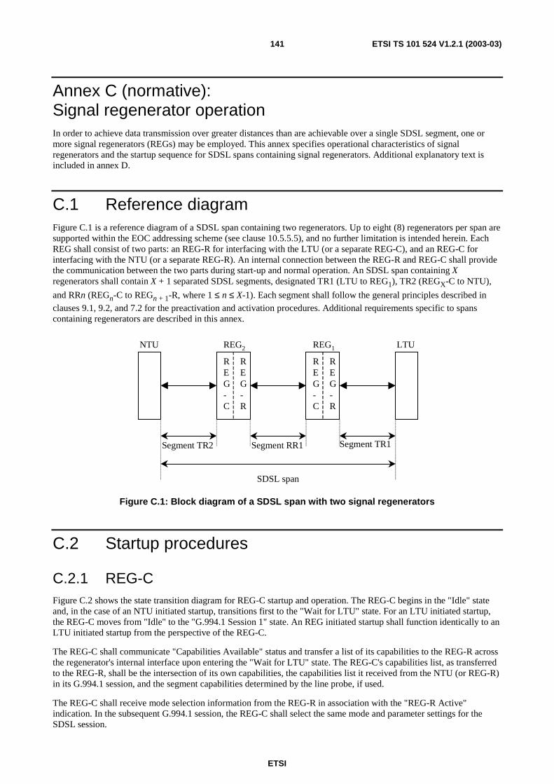
ETSI
ETSI TS 101 524 V1.2.1 (2003-03) 141
Annex C (normative): Signal regenerator operation In order to achieve data transmission over greater distances than are achievable over a single SDSL segment, one or more signal regenerators (REGs) may be employed. This annex specifies operational characteristics of signal regenerators and the startup sequence for SDSL spans containing signal regenerators. Additional explanatory text is included in annex D.
C.1 Reference diagram Figure C.1 is a reference diagram of a SDSL span containing two regenerators. Up to eight (8) regenerators per span are supported within the EOC addressing scheme (see clause 10.5.5.5), and no further limitation is intended herein. Each REG shall consist of two parts: an REG-R for interfacing with the LTU (or a separate REG-C), and an REG-C for interfacing with the NTU (or a separate REG-R). An internal connection between the REG-R and REG-C shall provide the communication between the two parts during start-up and normal operation. An SDSL span containing X regenerators shall contain X + 1 separated SDSL segments, designated TR1 (LTU to REG1), TR2 (REGX-C to NTU),
and RRn (REGn-C to REGn + 1-R, where 1 ≤ n ≤ X-1). Each segment shall follow the general principles described in clauses 9.1, 9.2, and 7.2 for the preactivation and activation procedures. Additional requirements specific to spans containing regenerators are described in this annex.
NTU
REG-C
REG-R
REG-C
REG-R
Segment RR1 Segment TR1Segment TR2
SDSL span
REG2 REG1 LTU
Figure C.1: Block diagram of a SDSL span with two signal regenerators
C.2 Startup procedures
C.2.1 REG-C Figure C.2 shows the state transition diagram for REG-C startup and operation. The REG-C begins in the "Idle" state and, in the case of an NTU initiated startup, transitions first to the "Wait for LTU" state. For an LTU initiated startup, the REG-C moves from "Idle" to the "G.994.1 Session 1" state. An REG initiated startup shall function identically to an LTU initiated startup from the perspective of the REG-C.
The REG-C shall communicate "Capabilities Available" status and transfer a list of its capabilities to the REG-R across the regenerator's internal interface upon entering the "Wait for LTU" state. The REG-C's capabilities list, as transferred to the REG-R, shall be the intersection of its own capabilities, the capabilities list it received from the NTU (or REG-R) in its G.994.1 session, and the segment capabilities determined by the line probe, if used.
The REG-C shall receive mode selection information from the REG-R in association with the "REG-R Active" indication. In the subsequent G.994.1 session, the REG-C shall select the same mode and parameter settings for the SDSL session.

ETSI
ETSI TS 101 524 V1.2.1 (2003-03) 142
The timer TREGC shall be set to 4 minutes. If TREGC expires before the REG-C reaches the "Active" state, the REG-C
shall return to the "Idle" state and shall indicate link failure to the REG-R across the internal interface. The REG-C shall also indicate failure and return to the "Idle" state if a G.994.1 initiation is unsuccessful after 30 s.
The "Diagnostic Mode" bit, if set in the G.994.1 Capabilities Exchange, shall cause an REG-C to function as an LTU if the subsequent segment fails. This implies that an internal failure indication received while in the "Wait for LTU" state shall cause the REG-C to select an operational mode, initiate a G.994.1 session, and transition to state "G.994.1 Session 2".
Idle
G.994.1failure
Receive internal“Link initiation” Indication
Initiate G.994.1 Session
Receive MS with “silent period” = 1
Complete G.994.1 SessionStart TREGC
Receive G.994.1 InitiationG.994.1 Session
Capabilities Exchange(Line Probe)
(second G.994.1 Session)(Capabilities Exchange)
Send MS with “Silent Period” = 1Restart TREGC
Receive Capabilities ExchangeCapabilities Exchange
(Line Probe)(second G.994.1 Session)(Capabilities Exchange)
Send MS with “Silent Period” = 1Restart TREGC
Internal FailureIndication and
Diagnostic ModeInitiate G.994.1
Session
Receive Internal“REG-R Active” Indication
Initiate G.994.1 Session
Complete G.994.1 Sessionwith Mode Selection
SDSL Activation
Disconnect,Failure or Retrain
Receive Internal“REG-R Active” Indication
Initiate G.994.1 Session
Receive G.994.1 InitiationG.994.1 Session
MS with “Silent Period” = 1
Receive G.994.1 InitiationG.994.1 Session
Capabilities Exchange(Line Probe)
(second G.994.1 Session)(Capabilities Exchange)
Send MS with “Silent Period” = 1Restart TREGC
G.994.1Failure
Internal FailureIndication andnot DiagnosticMode
TREGCTimeout
TREGCTimeout
G.994.1 Session 1
Wait for NTU
Wait for LTU
G.994.1 Session 2
Active
Figure C.2: REG-C state transition diagram
C.2.2 REG-R Figure C.3 shows the state transition diagram for REG-R startup and operation. The REG-R begins in the "Idle" state and, in the case of an NTU initiated train, transitions first to the "G.994.1 Session 1" state. For an LTU initiated train, the REG-C moves from "Idle" to the "G.994.1 Session 2" state.
The REG-R shall communicate "Link Initiation" status to the REG-C across the regenerator"s internal interface upon entering the "Wait for NTU" state. Upon entering the "Active" state, it shall communicate "REG-R Active" status to the REG-C. If plesiochronous operation (Clock mode 1; see clause 10) is selected, the REG-R may optionally indicate its entry into the "Active" state to the REG-C prior to the completion of the SDSL activation sequence. If synchronous or network referenced plesiochronous clocking is selected (Clock modes 2, 3a, or 3b; see clause 10), the REG-R shall not indicate entry into the "Active" state until the SDSL activation sequence has been completed.

ETSI
ETSI TS 101 524 V1.2.1 (2003-03) 143
The REG-R shall receive a list of capabilities from the REG-C across the regenerator's internal interface in association with the "Capabilities Available" indication. The REG-R's capabilities list, as indicated in the subsequent G.994.1 session, shall be the intersection of its own capabilities with the capabilities list it received from the REG-C.
The REG-R shall provide mode selection information to the REG-C in association with the "REG-R Active" indication, based on the selections it has received in the G.994.1 session.
The timer TREGR shall be set to 4 minutes. If TREGR expires before the REG-R reaches the "Active" state, the REG-R shall return to the "Idle" state and shall indicate link failure to the REG-C across the internal interface. The REG-R shall also indicate failure and return to the "Idle" state if a G.994.1 initiation is unsuccessful after 30 s.
The "Diagnostic Mode" bit, if set in the G.994.1 Capabilities Exchange, shall cause an REG-R to function as an NTU if the subsequent segment fails. This implies that an internal failure indication received while in the "Wait for NTU" state shall cause the REG-R to initiate a G.994.1 session and transition to state "G.994.1 Session 2".
TREGRTimeout
IdleReceive G.994.1 Initiation
Begin G.994.1 SessionSend MS with
“Silent Period” = 1
Receive Ack(1)Complete G.994.1 Session
Start TREGR
Receive G.994.1 InitiationG.994.1 Session
Send MS with “Silent Period” = 1
Start G.994.1 Session NormallyCapabilities Exchange
(Line Probe)(second G.994.1 Session)(Capabilities Exchange)
Internal FailureIndication and
Diagnostic ModeInitiate G.994.1
Session
Receive REQ-MRSelect Mode
SDSL Activation
Receive Mode SelectionSDSL Activation
Disconnect,Failure or Retrain
Receive Internal“Capabilities Available” Indication
Initiate G.994.1 Session
Receive G.994.1 InitiationSelect Mode
SDSL Activation
G.994.1Failure
Internal FailureIndication andnot DiagnosticMode
TREGRTimeout
G.994.1 Session 1
Wait for NTU
G.994.1 Session 2
Active
Check for Start
Wait for LTU
Receive Internal“Capabilities Available” Indication
Initiate G.994.1 Session
Receive MS“Silent Period” = 1
Start TREGR
Figure C.3: REG-R state transition diagram
C.2.3 LTU In order to support operation with regenerators, each LTU shall support the Regenerator Silent Period (RSP) bit, as specified in ITU-T Recommendation G.994.1 [16]. Second, the LTU shall not indicate a training failure or error until it has been forced into "silent" mode for at least 5 consecutive minutes.

ETSI
ETSI TS 101 524 V1.2.1 (2003-03) 144
C.2.4 NTU In order to support operation with regenerators, each NTU shall support the Regenerator Silent Period (RSP) bit, as specified in ITU-T Recommendation G.994.1 [16]. The NTU shall not indicate a training failure or error until it has been forced into "silent" mode for at least 5 consecutive minutes.
C.2.5 Segment failures and retrains In the case of a segment failure or a retrain, each segment of the span shall be deactivated, with each REG-C and each REG-R returning to its "Idle" state. The restart may then be initiated by the REG, the NTU, or the LTU.
C.3 Symbol rates Signal regenerators may transmit at symbol rates up to and including 685,33 ksymbol/s. This corresponds, for 16-TCPAM, to maximum user data rates (not including framing overhead) of 2,048 Mbit/s. Operation at higher symbol rates is for further study.
Each TU and REG on a span shall select the same operational data rate.
C.4 PSD masks Any of the PSDs may be used for the TR1 segment (LTU to REG1-R). All other segments shall employ one of the
appropriate symmetric PSDs, as described in clause 9.4.1. The selection of PSD shall be limited by the symbol rate considerations of clause C.3.

ETSI
ETSI TS 101 524 V1.2.1 (2003-03) 145
Annex D (normative): Deactivation and warm-start procedure Support of the reduced power mode, the deactivation and the warm-start is optional.
NOTE: Frequent transitions to/from the reduced power mode introduce a non-stationary noise environment, whose effect on deployed xDSL systems is not fully known. Because of this, regional access restrictions regarding this procedure might apply.
D.1 Deactivation to reduced power mode This clause describes waveforms at the loop interface and associated procedures during deactivation. Figure D.1 illustrates the deactivation sequence.
The deactivation can be initiated by the NTU or by the LTU. EOC signalling is used to initiate the deactivation. The initiating side is called unit A, the other side shall be called unit B.
The standard sequence is as follows: Upon receiving the eoc-message "Deactivation Request", unit B responds by the eoc-message "Deactivation Acknowledge" or by "Unable To Comply (UTC)". After sending the "Deactivation Acknowledge' containing an acceptance to the deactivation (bit OK = "1"), unit B continues transmitting and waits for the deactivation of unit A. After receiving the acceptance to the deactivation request, unit A stops transmitting and enters the reduced power mode. After detecting that unit A has stopped transmitting, e.g. by detecting an LOSW-error, unit B stops transmitting and enters the reduced power mode as well.
The eoc messages "Deactivation Request" and "Deactivation Acknowledge" indicate the ability of the sender for the deactivation to the reduced power mode and a subsequent warm-start.

ETSI
ETSI TS 101 524 V1.2.1 (2003-03) 146
unit A unit B
freezecoefficients
freezecoefficients
ceasetransmission
ceasetransmission
DeactivationRequest
DeactivationIndication
no signal
no signal
LOSWdefect
powerdown
powerdown
eoc messageDeactivation Request
DeactivationIndication
eoc message DeactivationAcknowledge
TPS-TCLayer
TPS-TCLayer
Figure D.1: Deactivation sequence
D.1.1 Void
D.1.2 Deactivation sequence With messages "Deactivation Request" and "Deactivation Acknowledge", however, each transceiver can also inhibit or stop an initiated deactivation process by setting bit OK to "0" in the relevant eoc-message. This is useful when during or after the transmission of the "Deactivation Request" it becomes apparent that the data link is about to be used.
In warm-start the transmission shall be active to at least time tactive to minimize effects of nonstationary cross talk to systems sharing the same binder.
D.1.3 Deactivation EOC Messages
D.1.3.1 Deactivation Request – Management: Message
The Deactivation Request message is transmitted to request a deactivation or to withdraw an issued deactivation request. The destination address shall be F16 to indicate this is a broadcast message.

ETSI
ETSI TS 101 524 V1.2.1 (2003-03) 147
Table D.1: Deactivation request - Message ID 22
Octet # Contents Data Type Reference 1 22 Message ID 2 bits 7..1 Reserved set to 0 2 bit 0 Bit 0 OK 0 = Deactivation requested,
1 = Deactivation request cancelled
3 Reserved set to 0
D.1.3.2 Deactivation Response - Management message: Message
The deactivation response message is used to confirm the deactivation command or to refuse a deactivation request
Table D.2: Deactivation Acknowledge - Message ID 150
Octet # Contents Data Type Reference 1 150 Message ID 2 bits 7..1 Reserved set to 0 2 bit 0 OK 0 = Deactivation OK,
1 = Deactivation not possible
3 Reserved set to 0
D.2 Warm-start activation The warm-start can be initiated by the NTU or the LTU. This clause describes waveforms at the loop interface and associated procedures during warm-start. The direct specification of the performance of individual receiver elements is avoided when possible. Instead, the transmitter characteristics are specified on an individual basis and the receiver performance is specified on a general basis as the aggregate performance of all receiver elements. Exceptions are made for cases where the performance of an individual receiver element is crucial to inter-operability.
In contrast to the activation described in clause 9.1, a warm-start makes use of all settings stored in a previous successful activation to achieve a minimum start-up time. An activation is successful if convergence has been achieved and the data mode has been reached (see clause 9.3). All settings i.e. negotiated configuration in the preactivation, all data in the activation frame and all values in adaptive filters have to be stored before deactivating the transmission. The warm-start relies on the fact that all previously stored settings such as the transfer characteristics of the receive and transmit path and the timing relation between receive and transmit signals are still relevant. Small changes .e.g. due to variations of ambient temperature should not inhibit the warm-start activation. However, if the equipment or the loop characteristics have changed significantly, the warm-start activation may fail and a cold-start will be performed instead.
D.2.1 Warm-start activation PMD reference model The block diagram of the warm-start activation PMD layer of an LTU and NTU transmitter is shown in figure D.2.
logical zeros
t(m)
d0(m)
logical ones d1(m)
Scrambler s(m) Mapper x(m)ChannelPrecoder
y(m)SpectralShaper
z(t)
PACCoutput at
loopinterface
Figure D.2: Warm-start activation PMD reference model

ETSI
ETSI TS 101 524 V1.2.1 (2003-03) 148
The time index m represents the symbol time, and t represents analog time. Since activation uses 2-PAM modulation, the bit time is equivalent to the symbol time. The output of the scrambler is s(m). The output of the mapper is y(m), and the output of the spectral shaper at the loop interface is z(t). d1(m) is an initialization signal that shall be logical ones for all m. d0(m) is an initialization signal that shall be logical zeros for all m. The modulation format shall be Tomlinson-coded 2-level signal, with the full symbol rate selected for data mode operation. During activation the timing reference for the activation signals have a tolerance of ±32 ppm at the LTU and ±100 ppm at the NTU.
The output bits from the scrambler s(m) shall be mapped to an output level y(m) as follows:
Table D.3: Bit-to-level mapping
Scrambler output s(m) Mapper output level y(m) Data mode index 0 -9/16 0011 1 +9/16 1000
The levels corresponding to a 0 and 1 at the output of the scrambler shall be identical to the levels of the 16-TC-PAM constellation corresponding to indexes 0011 and 1000 respectively.
D.2.2 Warm-start activation sequence The sequence and timing diagram for the warm-start activation sequence is given in figure D.3.
tWUN tWUL
tWSact
tWS tWS
WWUN WSN WOKN Data
NTU in operationalstatus
WSL WOKL Data
LTU and NTU inoperational status
WWUL
NTU
LTU
only if activationinitiated by NTU
Half Duplex Segments
WECN
tWS tSYNtECN
Figure D.3: Timing diagram for the warm-start activation sequence

ETSI
ETSI TS 101 524 V1.2.1 (2003-03) 149
Table D.4: Duration and tolerances for activation signals
Signal Parameter Reference Nominal Value
Tolerance
tWUN Duration of WWUN D.2.4.1 12 ms ± 2 ms
tWS Guard time to prevent over lapping signals 6 ms ± 2 ms
tWUL Duration of WWUL D.2.4.2 20 ms ± 2 ms
tECN Duration of the half duplex segment of the NTU D.2.4.3 40 ms ± 2 ms
tSYN Minimum Duration of the half duplex segment of the LTU
100 ms ± 2 ms
tWSact
Maximum activation time 500 ms
tactive
Minimum time the link has to remain active 5 min
NOTE: The maximum time for activation, occurring after a deactivation without any intervening loopback or powering action and without any change in cable characteristic for a metallic pair cable transmission system is tWSact This value for activation time is understood as a 95 %-value when testing with line
models specified for the digital transmission system.

ETSI
ETSI TS 101 524 V1.2.1 (2003-03) 150
D.2.3 State transition diagram The state transition diagram for the warm-start activation of the NTU and the LTU is given in figure D.4.
*
PowerDown
WarmstartReq. by NTU
WWUN
Wait tWS
WSN
NTU converged
WOKN
WOKL detected
WarmstartException
state
Data
Pre-activation
* Exception condition(e.g. missed detection
of expected signal) *
*
*
PowerDown
Warmstart Req. by LTUor WWUN detected
WWUL
LTU converged andWOKN detected
WOKL
WarmstartException
state
Data
Pre-activation
* Exception condition(e.g. missed detection
of expected signal)
*
*
*
R-Tone detected
WWULdetected
WWUL
Activation of NTU Activation of LTU
C-Tone detectedWWUL
detected
WaittECN+2*tWS
WECN
WaittSYN+tWS
WSL
Figure D.4: LTU and NTU transmitter warm-start state transition diagram
D.2.4 Signals used in warm-start activation
D.2.4.1 Signal WWUN
The NTU initiated warm-start shall start with the NTU sending the warm-start wake up signal, WWUN for a duration of
tWUN. The waveform and the transmit power of WWUN is the same as of the 12 kHz-R-Tone used in the PACC.

ETSI
ETSI TS 101 524 V1.2.1 (2003-03) 151
D.2.4.2 Signal WWUL
The wake-up signal for the LTU initiated warm-start shall be the WWUL. If the warm-start is initiated by the NTU, the
LTU shall send the signal WWUL.after detecting the signal WWUN. WWUL shall have a duration of tWUL. The waveform
and the transmit power of WWUL is the same as of the 20 kHz-C-Tone used in the PACC.
D.2.4.3 Signal WECN
The NTU shall send WECN, beginning tWS after the end of WWUL. Waveform WECN shall be generated by connecting
logical ones to the input of the NTU scrambler as shown in figure D.2. The transmit power, symbol rate and PSD mask for WECN, shall be as for signal WSL
Half duplex signal WECN shall be sent for time tECN.
D.2.4.4 Signal WSL
The LTU shall send WSL beginning tWS after the end of WECN. Waveform WSL shall be generated by connecting logical ones to the input of the LTU scrambler as shown in figure D.2. The transmit power, symbol rate and PSD mask for WSL, shall be as negotiated during the preactivation sequence.
D.2.4.5 Signal WSN
The NTU shall start transmitting WSN beginning tWS + tSYN after the end of WECN. Waveform WSN shall be generated
by connecting logical ones to the input of the NTU scrambler as shown in figure D.2. The transmit power, symbol rate and PSD mask for WSN, shall be as negotiated during the preactivation sequence.
D.2.4.6 Signal WOKN
The NTU shall start transmitting WOKN when the NTU achieves full operational status. Full operational status of the
NTU means that the NTU is ready to enter data mode. Waveform WOKN shall be generated by connecting logical zeros
to the input of the NTU scrambler as shown in figure D.2. The transmit power, symbol rate and PSD mask for WOKN,
shall be as for signal WSN
D.2.4.7 Signal WOKL
The LTU shall send WOKL when the LTU has both detected WOKL and achieves full operational status. Full operational
status of the LTU means that the LTU is ready to enter data mode. Waveform WOKL shall be generated by connecting logical ones signal to the input of the LTU scrambler as shown in figure D.2. The transmit power, symbolrate and PSD mask for WOKL shall be the same as for WSL. WOKL shall be sent for exactly 256 symbols.
D.2.4.8 Datac and Datar
Within 200 symbols after the end of WOKL, the LTU shall send Datac and NTU shall send Datar. These signals are
described in clause 9.2. There is no required relationship between the end of WOKL and any bit within the SDSL data-
mode frame. The SDSL payload data shall be valid TPayloadValid (see table D.5) after the end of WOKL.
D.2.4.9 Warm-start exception-condition
An exception condition shall be declared during warm-start if the timeout values given in clause D.2.4.11 expire or if any vendor-defined abnormal event occurs.

ETSI
ETSI TS 101 524 V1.2.1 (2003-03) 152
D.2.4.10 Warm-start Exception-state
If an exception condition is declared during warm-start, the LTU or NTU enters the exception state and warm-start is aborted. During the exception state the TU shall be silent for at least TSilence (see table D.5), wait for transmission from
the far end to cease, then return to the corresponding initial startup state. The NTU and LTU shall begin preactivation, as per clause 9.2.
D.2.4.11 Timeouts
Table D.5 shows the system timeouts and their values.
Table D.5: Timeout values
Name Parameter Value TSilence Minimum time in the warm-start exception state where the LTU or
NTU are silent before the start of preactivation. See table 9.3
TPayloadValid Time from start of Datar and Datar to valid SDSL payload data See table 9.3

ETSI
ETSI TS 101 524 V1.2.1 (2003-03) 153
Annex E (informative): Signal regenerator startup description This annex describes the startup sequence used on spans employing regenerators. The sequence applies to spans with an arbitrary number of regenerators (up to 8), but for simplicity, the description here assumes a two-regenerator link. The use of line probing is optional, but its use is assumed for the purpose of this description.
The basic premise is that capability lists and line probe results propagate from the NTU toward the LTU and that the SDSL training begins at the LTU and propagates in the direction toward the NTU. The Regenerator Silent Period (RSP) bit in ITU-T Recommendation G.994.1 [16] is used to hold off segments while the startup process propagates across the span.
The block diagram in figure E.1 shows a typical SDSL span with two regenerators as a reference for the startup sequences described below.
NTU
REG-C
REG-R
REG-C
REG-R
Segment RR1 Segment TR1Segment TR2
SDSL span
REG2 REG1 LTU
Figure E.1: Block diagram of a SDSL span with two signal regenerators
E.1 NTU initiated startup In most typical SDSL installations, the NTU can be expected to initiate the startup process. The proposed SDSL startup process for NTU initiation is described in the text below and shown graphically in table E.1.
In this mode, the NTU triggers the startup process by initiating a G.994.1 session with the regenerator closest to it (over segment TR2). The NTU and the REG2-C then exchange capabilities and optionally perform a line probe and a second
capabilities exchange. The units do not have enough information to begin SDSL activation at this point, so the REG2-C
issues an MS with the RSP bit set to hold off the NTU while the startup process propagates across the span. The G.994.1 session terminates normally, and the NTU begins its waiting period.
Next, the REG2-C conveys the capabilities from Segment TR2 to the REG2-R across the regenerator's internal interface.
The REG2-R then initiates a G.994.1 session with the REG1-C and performs the same capabilities exchange and line
probing sequence described above for the first segment. The capabilities expressed by the REG2-R are the intersection of its own capabilities with the capabilities it has received for Segment TR2. The units still do not have sufficient information to begin SDSL activation, so, again, the REG1-R issues an MS with the RSP bit set. The G.994.1 session
terminates normally, and the REG2-R begins its waiting period.

ETSI
ETSI TS 101 524 V1.2.1 (2003-03) 154
As before, the REG1-C then conveys the capabilities from segment RR1 (including the information from segment TR2)
to the REG1-R across the regenerator's internal interface. The REG1-R initiates a G.994.1 session with the LTU and performs a capabilities exchange. Optionally, a line probe and a second capabilities exchange may be used. As before, the capabilities expressed by the REG1-R are the intersection of its own capabilities with the capabilities it has received for segments RR1 and TR2. At this point, the LTU possesses all of the required information to select the span's operational parameters. The data rate and other parameters are selected, just as in a normal (non-regenerator) preactivation sequence and then the SDSL activation begins for segment TR1.
When the LTU/REG1-R link (over segment TR1) has completed the SDSL activation sequence (or the G.994.1 session,
if clock mode 1 is selected), the REG1-R communicates the selected operational parameters to the REG1-C across the
regenerator's internal interface. At this point, the REG1-C initiates a G.994.1 session with the REG2-R over segment RR1. Parameters are selected - there should be no need for another CLR-CL exchange at this point - and the units perform the normal SDSL activation. If clock mode 1 is selected (classic plesiochronous) there is no need to lock symbol timing to a network clock reference. In this case, the REG1-C/REG2-R G.994.1 session and activation should
begin as soon as the LTU/REG1-R G.994.1 sessions completes. In clock modes 2, 3a, and 3b, such a network or data
clock reference is necessary for establishing symbol timing. In these modes, the REG1-C will delay the initiation of its
G.994.1 session until the LTU/REG1-R activation is complete. In this way, the required reference clock will be
available for symbol timing on the REG1-C/REG2-R segment.
When the REG1-C/REG2-R link (over segment RR1) has completed the SDSL activation sequence (or the G.994.1
session, if clock mode 1 is selected), the REG2-R communicates the selected operational parameters to the REG2-C
across the regenerator's internal interface. The REG2-C initiates a G.994.1 session with the NTU over Segment TR2. Parameters are selected and the units perform the normal SDSL activation. When this activation sequence is complete, the span can become fully operational.
Table E.1: NTU initiated startup sequence
Segment TR2 (NTU/REG2-C)
Segment RR1 (REG2-R/REG1-C)
Segment TR1 (REG1-R/LTU)
G.994.1 Start → Capabilities exchange Line probe Capabilities exchange ← MS (RSP) G.994.1 Start → Capabilities exchange Line probe Capabilities exchange ← MS (RSP) G.994.1 Start → Capabilities exchange Line probe Capabilities exchange Mode selection SDSL activation ← G.994.1 Start Mode selection SDSL activation ← G.994.1 Start Mode selection SDSL activation

ETSI
ETSI TS 101 524 V1.2.1 (2003-03) 155
E.2 LTU initiated startup In some cases, it may be desirable for the LTU to initiate the startup process. The proposed SDSL startup process for LTU initiation is described in the text below and shown graphically in table E.2.
In this mode, the LTU triggers the startup process by initiating a G.994.1 session with the regenerator closest to it (over segment TR1). The REG2-C issues an MS with the RSP bit set to hold off the LTU while the startup process propagates
across the span. The G.994.1 session terminates normally, and the LTU begins its wait period. Next, the REG1-C
initiates a G.994.1 session with the REG2-R, which, again is terminated following an MS from the REG2-R with the
RSP bit set.
The REG2-C next initiates a G.994.1 session with the NTU. From this point on, the start sequence is as described in
clause D.1 for the NTU initiated startup.
Table E.2: LTU initiated startup sequence
Segment TR2 (NTU/REG2-C)
Segment RR1 (REG2-R/REG1-C)
Segment TR1 (REG1-R/LTU)
← G.994.1 Start MS (RSP) → ← G.994.1 Start MS (RSP) → ← G.994.1 Start Capabilities exchange Line probe Capabilities exchange ← MS (RSP) G.994.1 Start → Capabilities exchange Line probe Capabilities exchange ← MS (RSP) G.994.1 Start → Capabilities exchange Line probe Capabilities exchange Mode selection SDSL activation ← G.994.1 Start Mode selection SDSL activation ← G.994.1 Start Mode selection SDSL activation
E.3 REG initiated startup In some limited applications (including some maintenance and retrain scenarios), it may be desirable for a regenerator to initiate the start sequence. In this mode, the REG will initiate the train in the downstream direction - i.e. toward the NTU in the same manner that it would have for the corresponding segment of the LTU Startup Procedure (as described in clause E.2). The NTU will then initiate the capabilities exchange and line probing procedure toward the LTU, as in a normal LTU initiated startup. The startup sequence begins with the initiating REG-C and propagating toward the NTU.

ETSI
ETSI TS 101 524 V1.2.1 (2003-03) 156
E.4 Collisions and retrains Collisions (equivalent to "glare" conditions in voice applications) can occur in cases where both the LTU and the NTU attempt to initiate connections simultaneously. Using the process described above, these collisions are resolved by specifying that R-to-C capabilities exchanges and probes will always take precedence over C-to-R train requests. G.994.1 sessions inherently resolve collisions on individual segments.
In G.994.1, the RSP timeout is specified as approximately 1 minute. For spans with no more than one regenerator, this is ideal. For multi-regenerator spans, however, a TU may time out and initiate a new G.994.1 session before the REG is prepared to begin the next phase of the train. In such cases, the REG should respond to the G.994.1 initiation and issue an MS message with the RSP bit set to hold off the TU once again. For its part, the REG should implement an internal timer and should not consider a startup to have failed until that timer has expired. The timer should be started when the REG receives a RSP bit in an MS message and should not expire for at least 4 minutes.
If any segment must retrain due to line conditions or other causes, each segment of the span shall be deactivated and the full startup procedure shall be re-initiated.
E.5 Diagnostic mode activation If a segment fails, the startup procedure will also fail for the entire span. This would normally be characterized at the TU by being told to enter a silent interval via the RSP bit and never receiving another G.994.1 request. Without some diagnostic information, the service provider would have no easy way to test the integrity of the various segments.
This concern is resolved by the use of the "Diagnostic Mode" in G.994.1 to trigger a diagnostic training mode. This bit, when set, causes an REG connected to a failed segment to act as a TU and allow the startup procedure to finish. In this way, all of the segments before the failed segment may be tested using loopbacks and EOC-initiated tests. This would allow network operators to quickly isolate the segment where the failure has occurred.

ETSI
ETSI TS 101 524 V1.2.1 (2003-03) 157
Annex F (informative): Typical characteristics of cables The primary cable parameters Zs = Rs + jω·Ls and Yp = 0 + jω·Cp per unit length are specified for various frequencies in tables F.1 and F.2. They are based on existing RLCG tables specified in the HDSL specification [1], and extended up to 2 MHz. The values of the RLC parameters for other frequencies can be found by using a "cubic spline interpolation".
Table F.1: Line constants for the cable sections in the SDSL testloops
SDSL.PE04 SDSL.PE05 SDSL.PE06 SDSL.PE08 freq [Hz]
Rs [ΩΩΩΩ/m]
Ls [H/m]
Cp [F/m]
Rs [ΩΩΩΩ/m]
Ls [H/m]
Cp [F/m]
Rs [ΩΩΩΩ/m]
Ls [H/m]
Cp [F/m]
Rs [ΩΩΩΩ/m]
Ls [H/m]
Cp [F/m]
× 10+3 × 10-3 × 10-9 × 10-12 × 10-3 × 10-9 × 10-12 × 10-3 × 10-9 × 10-12 × 10-3 × 10-9 × 10-12 0 268 680 45,5 172 680 25 119 700 56 67 700 37,8
10 268 678 45,5 172 678 25 120 695 56 70,0 700 37,8 20 269 675 45,5 173 675 25 121 693 56 72,5 687 37,8 40 271 669 45,5 175 667 25 125 680 56 75,0 665 37,8
100 282 650 45,5 190 646 25 146 655 56 91,7 628 37,8 150 295 642 45,5 207 637 25 167 641 56 105 609 37,8 200 312 635 45,5 227 629 25 189 633 56 117 595 37,8 400 390 619 45,5 302 603 25 260 601 56 159 568 37,8 500 425 608 45,5 334 592 25 288 590 56 177,5 560 37,8 700 493 593 45,5 392 577 25 340 576 56 209 553 37,8
1 000 582 582 45,5 466 572 25 405 570 56 250 547 37,8 2 000 816 571 45,5 655 565 25 571 560 56 353 540 37,8
Table F.2: Line constants for the cable sections in the SDSL testloops
SDSL.PVC032 SDSL.PVC04 SDSL.PVC063 freq [Hz]
Rs [ΩΩΩΩ/m]
Ls [H/m]
Cp [F/m]
Rs [ΩΩΩΩ/m]
Ls [H/m]
Cp [F/m]
Rs [ΩΩΩΩ/m]
Ls [H/m]
Cp [F/m]
× 10+3 × 10-3 × 10-9 × 10-12 × 10-3 × 10-9 × 10-12 × 10-3 × 10-9 × 10-12 0 419 650 120 268 650 120 108 635 120
10 419 650 120 268 650 120 108 635 120 20 419 650 120 268 650 120 108 635 120 40 419 650 120 268 650 120 111 630 120
100 427 647 120 281 635 120 141 604 120 150 453 635 120 295 627 120 173 584 120 200 493 621 120 311 619 120 207 560 120 400 679 577 120 391 592 120 319 492 120 500 750 560 120 426 579 120 361 469 120 700 877 546 120 494 566 120 427 450 120
1 000 1 041 545 120 584 559 120 510 442 120 2 000 1 463 540 120 817 550 120 720 434 120

ETSI
ETSI TS 101 524 V1.2.1 (2003-03) 158
Annex G (informative): Transmission and reflection of cable sections
G.1 Definition of transfer function and insertion loss Transfer function and insertion loss are quantities that are related to the values of the (complex) source and load impedance. Within the context of the present document, a simplified definition is used in which source and load are the same and equal to a real value RV. The transfer function and insertion loss associated with a two-port network,
normalized to a chosen reference resistance RV, are defined as the following voltage ratios (see figures G.1 and G.2):
Transfer Function = 1
2
U
U
Insertion Loss = 2
1
U
U
RV
RV
+
-U1
Figure G.1: Voltage across the load
Two-portNetwork
RV
RV
+
-U2
Figure G.2: Voltage across the load with a two-port network inserted
These quantities are directly related to the scattering parameters associated with the two-port network as defined in clause G.2:
Transfer Function (TF) = s21 Magnitude of TF (in dB) = 20 log10(|s21|)
Insertion Loss (IL) = 1/s21 Magnitude of IL (in dB) = -20 log10(|s21|)

ETSI
ETSI TS 101 524 V1.2.1 (2003-03) 159
G.2 Derivation of s-parameters from primary cable parameters
The testloops are defined by one or a cascade of cable sections. The characteristics of each section are specified by means of primary cable parameters Zs, Yp per unit length (L0). This clause gives the equations to evaluate the relevant characteristics of cable sections (s-parameters) from the primary parameters and to handle cascade of cable sections.
Insertion loss and return loss of a cable section, for SDSL, can be calculated from the primary parameters Zs, Yp per
unit length (L0) by evaluating the two-port s-parameters, normalized to RV = 135 Ω.
Zsx = (L/L0) · Zs γx = Zsx ·Ypx αx = real(γx) Rsx = real(Zsx) Gpx = real(Ypx)
Ypx = (L/L0) · Yp Z0 = Zsx /Ypx βx = imag(γx) Lsx = imag(Zsx/ω) Cpx = imag(Ypx/ω)
S =
2221
1211
ss
ss = ) )(( 2tanh//
1
00 +⋅+ xvv ZRRZ γ ×
) )((( ) ( )
( )( )
⋅−⋅−
x
x
vvx
xvv
ZRRZ
ZRRZ
γγ
γγ
tanh//cosh/2
cosh/2tanh//
00
00
Insertion Loss: 1/s21
Return Loss: 1/s11
The s-parameters of two cable sections (a and b) in cascade, Sab, can be calculated from the s-parameters Sa and Sb as
described below:
Sab =
2221
1211
ss
ss = ⋅
⋅− ba ss 11221
1
⋅∆−⋅⋅⋅∆−
asbbba
abbsaa
ssss
ssss
22222121
12121111 ∆si = s11i·s22i - s12i·s21i

ETSI
ETSI TS 101 524 V1.2.1 (2003-03) 160
Annex H (informative): Guideline for the narrowband interfaces implementation in the SDSL NTU This annex provides information needed for the implementation of power efficient narrowband interfaces (at the SDSL NTU) when lifeline service has to be guaranteed.
Narrowband interfaces and conditions that were taken into account are:
• ISDN user-network interface (S-interface);
• Analogue interface (PSTN) in the following conditions:
- "On Hook" with ringing applied;
- "On Hook" with no transmission and normal battery applied;
- "Off Hook", normal talk state;
- "On Hook", with FSK/DTMF data transfer;
- "Power denial".
The PSTN interface has been identified as the highest power consuming interface and, in particular, the operational state "Off Hook", normal talk state.
The following tables provide a guideline to the implementation of voice-band analogue interfaces (a/b interfaces) offered to the final user by means of adapter devices terminating various types of digital networks such as xDSL or ISDN. Particular attention is given to the power budget implied by the individual requirements.
The information was derived from EG 201 185 [13], ES 201 970 (see bibliography) and experience gained in the use of intelligent ISDN Network Terminations widely used for the ISDN network (NTs providing analogue terminal adapter interfaces to the user). The tables allow a comparison between those two ETSI documents in order to facilitate the harmonization of the network side of the analogue voice band switched interface (PSTN). The suggested values are very close to EG 201 185 [13], however they add important information on parameters affecting the power consumption (vital for the lifeline service) that are lacking in those documents.
General EG 201 185 (V1.1.1) ES 201 970 (V1.1.1) Suggested values notes
applicability (loop length) ≤ 100 Ω ≤ 750 Ω ≤ 100 Ω mechanical aspects RJ-11 (3 and 4) RJ-11 (3 and 4) RJ-11 Signalling on-hook voltage (min, max) 38 V to 78 V @100 kΩ
38 V to 78 V @ 100 MΩ/LF
38 V to 78 V @ 1 mA 1
on-hook voltage @ 2,5 mA ≥ 32 V ≥ 32 V ≥ 32 V 2
off-hook resistance (d.c.) n.a. n.a. ≤ 800 Ω 3 non-seizure current Iloop < 3 mA Iloop < 3 mA Iloop < 4 mA
seize current Iloop ≥ 6 mA Iloop ≥ 10 mA Iloop > 6 mA 4 seize surely recognized 150 ms 150 ms ≥ 250 ms
seize surely not recognized ≤ 25 ms ≤ 25 ms ≤ 50 ms
loop current (min-max) ≥ 18 mA 18 mA to 70 mA ≥ 18 mA @ 800 Ω ≥ 25 mA @ 400 Ω
loop current (recommended) 32 mA ± 7 mA 25 mA to 40 mA See line above
clear signal threshold ≤ 1 mA ≤ (seize curr. -0.5 mA) ≤ 6 mA
clear signal not recognized ≤ 350 ms ≤ 250 ms ≤ 150 ms
clear signal recognized ≥ 500 ms ≥ 500 ms ≥ 200 ms

ETSI
ETSI TS 101 524 V1.2.1 (2003-03) 161
clear signal from the network
release tone release tone release tone 5
EG 201 185 (V1.1.1) ES 201 970 (V1.1.1) Suggested values notes Signalling DTMF recognition level -5 dBV to -15 dBV -5 dBV to -15 dBV -5 dBV to -15 dBV
DTMF max twist 4 dB 6 dB 4 dB
DTMF frequency error ± (1,5 % + 2 Hz) ± (1,5 % + 2 Hz) ± (1,5 % + 2 Hz)
DTMF min duration 40 ms 40 ms 40 ms
DTMF min pause 40 ms 40 ms 40 ms
Ringing voltage (required)
≥ 35 Vrms @ 4 kΩ (a.c.) ≥ 35 Vrms @ 400 kΩ//LF ≥ 40 Vrms (2 KΩ, ϕ ≥ 60°) 6
Ringing frequency 25 Hz (or 50 Hz) ± 2 Hz 25 Hz (or 50 Hz) ± 2 Hz 25 Hz (or 50 Hz) ± 2 Hz
Distortion ≤ 5 %, symmetric ≤ 5 %, symmetric 10 %, symmetric
Max ringing current n.a. n.a. 80 mA
Superimposed d.c. 38 V to 78 V (optional) 38 V to 78 V (optional) 38 V to 78 V 7
Ring Trip threshold dc seize condition or ≤ 700 Ω (@ 25 Hz or 50 Hz)
dc seize condition or < 700 Ω @ 25 Hz
dc seize
Ring Trip Delay ≤ 100 ms ≤ 200 ms ≤ 200 ms
Tone level -18 dBV ± 6 dB -18 dBV ± 6 dB -18 dBV ± 6 dB
Signal quality
Impedance 270 Ω + (750 Ω//150 nF) 270 Ω + (750 Ω//150 nF) 270 Ω + (750 Ω//150 nF)
return loss
200 Hz to 500 Hz: 14-18 dB 500 Hz to 2 500 Hz: > 18 dB 2 000 Hz to 3 800 Hz: 18 dB to 14 dB
200 Hz to 300 Hz: > 8 dB 300 Hz to 500 Hz: 8 dB to 10 dB 500 Hz to 1 250 Hz: 10 dB to14 dB 1 250 Hz to 3 400 Hz: >14 dB 3 400 Hz to 3 800 Hz: 14 dB to 12 dB
200 Hz to 500 Hz:14 dB to18 dB 500 Hz to 2 500 Hz: >18 dB 2 000 Hz to 3 800 Hz: 18 dB to14 dB
8
balance to earth 200 Hz to 3 800 Hz: > 46 dB
50 Hz: >40 dB 200 Hz to 600 Hz: >40 dB 600 Hz to 3 800 Hz: >46 dB
50 Hz: > 20 dB 200 Hz to 600 Hz: > 40 dB 600 Hz to 3 800 Hz: >46 dB
input relative level +4 dBr ± 1 dB +4 dBr ± 2 dB +4 dBr ± 1 dB 9
output relative level -11 dBr ± 1 dB -11 dBr ± 2 dB -11 dBr ± 1 dB
Frequency Response
300 Hz: -0,3 to +1,0 dB 400 Hz: -0,3 to +0,75 dB 0,6 ÷ 2 kHz: -0,3 dB to +0,75 dB 2,4 kHz: -0,3 dB to +0,45 dB 3 kHz: -0,3 dB to +0,7 dB 3,4 kHz: -0,3 dB to +1,7 dB
as per ITU-T Q.552 as per ITU-T Q.552
loss vs. signal level see table 4 as per ITU-T Q.552 as per ITU-T Q.552
input levels 3,14 dB over nominal level 1,8 Vrms (+5,7 dBm) 3,14 dB over nominal level
receive noise ≤ -67 dBVp as per Q.552 -64 dBm0p
transmit noise ≤ -64 dBm0p as per Q.552 -64 dBm0p
absolute delay ≤ 2 ms n.a. ≤1,5 ms
relative delay (relative to the minimum)
500 Hz to 600 Hz: ≤1,8 ms 600 Hz to 1 000 Hz: ≤0,9 ms 1 000 Hz to 2 600 Hz: ≤0,3 ms 2 600 Hz to 2 800 Hz: ≤1,5 ms
n.a.
500 Hz to 600 Hz: ≤ 0,9 ms 600 Hz to 1 000 Hz: ≤0,45 ms 1 000 Hz to 2 600 Hz: ≤0,15 ms 2 600 Hz to 2 800 Hz: ≤0,75 ms
Optional features
Pulse dialling rate 8 to 12 pulse/s 8 to 12 pulse/s 8 to 12 pulse/s
break/pulse ratio 50 % to 75 % 50 % to 75 % 50 % to 75 %
Interdigit Pulse ≥240 ms ≥240 ms ≥240 ms
Register Recall 50 ms to 130 ms 50 ms to 130 ms 25 ms to 150 ms Hook Flash 75 ms to 850 ms n.a. n.a. 10
Metering Pulses frequency 12 kHz or 16 kHz 12 kHz or 16 kHz 12 kHz or 16 kHz
Metering Pulses level approx. 500 mVrms approx. 100 mVrms ≥200 mVrms
ETSI
ETSI TS 101 524 V1.2.1 (2003-03) 162
NOTE 1: A concept present in ES 201 970 is the Loading Factor (LF). The operator must state a single LF number for the Network Termination Point (NTP). Based on this LF information, the user can determine the number or the type of terminals that can be connected at the NTP. The operator must guarantee a minimum LF of 100. The single LF number stated by the operator is the minimum value among the LF calculated for four key parameters: the resistance to ground, the DC resistance in quiescent conditions, the ringing voltage, and the DC current during ringing. A skilled user may take advantage of the operator providing individual L's for these parameters. As an example, the ringing voltage is specified to be greater than 35 Vrms at a load of 400 kΩ/LF. If the operator specifies a LF of 100, this means that the 35 Vrms are guaranteed across a load of 4 kΩ.
NOTE 2: Meeting this value is an optional feature required to support ALASS services. NOTE 3: 800 Ω represents the sum of the loop and the terminal resistance (d.c.). NOTE 4: There is an additional recommendation (mentioned in EG 201 185 [13] and in ES 201 970): during any
transient state in the transition from quiescent to loop state, the NTP should be able to supply at least 4 mA over a 5 kΩ load for at least 20 ms. The reason for this requirements is that some TE may expect the full current immediately after going off-hook while some NTP may use high resistance supply to provide quiescent state "high" battery voltage (e.g. 50 V through a 10 kΩ resistance) and will not able to deliver the full current before switching in a lower value DC "battery" voltage. The combination of the two cases may cause problems, and the recommendation for the NTP is paired with a recommendation for the TE to be developed so that they can correctly seize the loop under this limited current transient.
NOTE 5: Polarity reversal or K-break may be required by some operators, additionally to release tones. NOTE 6: EG 201 185 [13] recommends supplying 35 Vrms over 2 kΩ, ac coupled. NOTE 7: A note specifies that TBR21 compliant devices are not guaranteed to operate with ringing sources without a
superimposed DC voltage. NOTE 8: For ES 201 970 (see bibliography), return loss measurements include the loop between the NTP and the
"line card". It is also stated than the specified value for the return loss at low-mid frequency may not be achieved for loop resistance ≥ 750 Ω.
NOTE 9: Including loop loss for ES 201 970 (see bibliography). NOTE 10: As a network option, the hook flash is an alternative to register recall. When hook-flash is used, the
minimum recognition time for clear originated from the TE raises to 950 ms to 1 050 ms.
ALASS services
Common ALASS services include provision of Calling Line Identity (CLI) and Message Waiting Indication (MWI).
These services are delivered to the terminal equipment using voice-band data, either during incoming call set-up, while the terminal is in the quiescent state or in the off-hook state (e.g. CLI during a CW offering). See EN 300 659-1, EN 300 659-2 and ES 200 778 (see bibliography).
In order to support ALASS services to the TE, the equipment should be able to support one or more additional features, such as:
a) control of polarity reversal;
b) a single burst of ringing current, with or without polarity reversal;
c) provision of 2,5 mA @ 32 V in the quiescent state;
d) ignore on-line d.c. current pulses not exceeding 25 ms duration;
e) generation of DTMF digits to the TE.

ETSI
ETSI TS 101 524 V1.2.1 (2003-03) 163
Annex I (informative): Tabulation of the noise profiles Annex I tabulates the total noise profile (sum of self and alien) corresponding to 0dB of margin for all the test cases. Those noise PSDs were used during the theoretical computation of the margin. The tabulated noise profiles should be measured into the calibrating impedance (see clause 12.2.3.1).
Noise Profile Nomenclature: ABBBCDE
A: Side (either C or R)
BBB: Rate
C: PSD type (either s for symmetric or a for asymmetric)
D: Noise Type (A ,B, C or D)
E: Loop Number (from 2 to 7).
The noise shapes used for test #1 will be identical to Noise A of test #2
Table I.1: LT side/symmetric PSDs
Noise profile
Magnitude of the noise in dBm per Hz (sign is always negative) as a function of frequency in kHz
1 10 20 30 40 50 60 70 80 90 100 150 200 250 300 350 400 600 800
C384sA2 114,9 99,2 95,0 93,1 92,5 92,3 92,9 93,9 93,4 92,7 92,0 88,1 86,3 85,0 83,8 82,9 82,1 79,4 77,6
C384sC2 120,6 104,6 100,4 98,4 97,7 97,6 98,7 101,8 102,6 102,0 101,3 94,5 92,7 91,4 90,2 89,3 88,5 87,8 86,8
C384sD2 131,8 104,4 99,5 97,1 95,8 95,3 96,4 100,5 107,0 114,2 121,6 138,0 138,0 138,0 138,0 138,0 138,0 138,0 138,0
C512sA2 114,9 99,4 95,3 93,4 92,8 92,3 92,0 91,9 92,0 92,2 91,9 88,1 86,3 85,0 83,8 82,9 82,1 79,4 77,6
C512sC2 120,6 104,9 100,8 98,8 98,1 97,7 97,4 97,5 98,3 100,0 100,9 94,5 92,7 91,4 90,2 89,3 88,5 87,8 86,8
C512sD2 132,8 105,6 100,6 98,0 96,4 95,4 94,8 94,8 95,8 98,7 103,2 131,4 138,0 138,0 138,0 138,0 138,0 138,0 138,0
C768sA2 114,9 99,6 95,6 93,7 93,3 92,8 92,4 91,9 91,2 90,7 90,3 88,1 86,3 84,9 83,8 82,9 82,1 79,4 77,6
C768sC2 120,6 105,2 101,2 99,3 98,8 98,4 98,0 97,5 97,0 96,6 96,4 94,4 92,7 91,4 90,2 89,3 88,5 87,8 86,8
C768sD2 134,2 107,3 102,2 99,5 97,7 96,5 95,5 94,8 94,3 93,9 93,8 102,6 120,9 138,0 138,0 138,0 138,0 138,0 138,0

ETSI
ETSI TS 101 524 V1.2.1 (2003-03) 164
Noise profile
Magnitude of the noise in dBm per Hz (sign is always negative) as a function of frequency in kHz
1 10 20 30 40 50 60 70 80 90 100 150 200 250 300 350 400 600 800
C1024sA2 114,9 99,7 95,7 93,9 93,6 93,2 92,8 92,3 91,5 90,8 90,3 87,5 86,3 84,9 83,8 82,9 82,1 79,4 77,6
C1024sC2 120,6 105,3 101,4 99,6 99,2 99,0 98,7 98,2 97,5 96,9 96,4 93,5 92,7 91,4 90,2 89,3 88,5 87,8 86,8
C1024sD2 135,0 108,5 103,3 100,6 98,8 97,5 96,4 95,5 94,9 94,3 93,9 93,6 102,1 115,8 130,8 138,0 138,0 138,0 138,0
C1280sA2 114,9 99,7 95,8 93,9 93,8 93,5 93,1 92,6 91,8 91,1 90,4 87,3 86,0 84,9 83,8 82,9 82,1 79,4 77,6
C1280sC2 120,6 105,4 101,5 99,7 99,5 99,4 99,3 98,8 98,0 97,4 96,8 93,2 92,2 91,3 90,2 89,3 88,5 87,8 86,8
C1280sD2 135,7 109,4 104,3 101,5 99,7 98,3 97,2 96,3 95,5 94,9 94,4 92,8 94,0 101,7 112,6 124,2 136,9 138,0 138,0
C1536sA2 115,0 99,7 95,8 94,0 93,8 93,6 93,3 92,8 92,0 91,2 90,6 87,3 85,8 84,7 83,8 82,9 82,1 79,4 77,6
C1536sC2 120,6 105,4 101,5 99,8 99,6 99,7 99,7 99,3 98,5 97,8 97,2 93,3 91,9 91,1 90,2 89,3 88,5 87,8 86,8
C1536sD2 136,1 110,2 105,0 102,3 100,4 99,0 97,9 96,9 96,1 95,5 94,9 92,9 92,3 94,4 101,4 110,4 119,9 138,0 138,0
C2048sA2 115,0 99,7 95,7 93,9 93,8 93,6 93,3 92,8 91,9 91,2 90,5 87,2 85,5 84,3 83,5 82,8 82,1 79,4 77,6
C2048sC2 120,6 105,4 101,5 99,8 99,6 99,7 99,7 99,4 98,5 97,8 97,2 93,1 91,6 90,4 89,7 89,2 88,5 87,8 86,8
C2048sD2 136,3 110,4 105,2 102,5 100,6 99,1 98,0 97,0 96,2 95,5 94,8 92,6 91,3 90,7 91,2 94,1 99,8 128,9 138,0
C2304sA2 115,0 99,7 95,8 94,0 93,8 93,6 93,4 92,9 92,0 91,2 90,6 87,2 85,5 84,3 83,4 82,7 82,0 79,4 77,6
C2304sC2 120,6 105,4 101,5 99,8 99,7 99,9 100,0 99,7 98,8 98,1 97,4 93,2 91,6 90,4 89,5 88,9 88,4 87,8 86,8
C2304sD2 136,6 110,9 105,7 102,9 101,0 99,6 98,4 97,4 96,6 95,9 95,3 92,9 91,5 90,7 90,4 91,3 94,4 118,1 138,0
C384sD3 131,8 104,4 99,5 97,1 95,8 95,3 96,4 100,5 107,0 114,2 121,6 138,0 138,0 138,0 138,0 138,0 138,0 138,0 138,0
C512sD3 132,8 105,6 100,6 98,0 96,4 95,4 94,8 94,8 95,8 98,7 103,2 131,4 138,0 138,0 138,0 138,0 138,0 138,0 138,0
C768sD3 134,1 107,3 102,2 99,5 97,7 96,5 95,5 94,8 94,3 93,9 93,8 102,6 120,9 138,0 138,0 138,0 138,0 138,0 138,0
C1024sD3 135,0 108,5 103,3 100,6 98,8 97,4 96,4 95,5 94,8 94,3 93,9 93,6 102,1 115,8 130,8 138,0 138,0 138,0 138,0
C1280sD3 135,6 109,4 104,2 101,5 99,7 98,3 97,2 96,2 95,5 94,9 94,3 92,8 94,0 101,7 112,6 124,2 136,9 138,0 138,0
C1536sD3 136,1 110,1 105,0 102,3 100,4 99,0 97,8 96,9 96,1 95,4 94,8 92,9 92,3 94,4 101,4 110,4 119,9 138,0 138,0

ETSI
ETSI TS 101 524 V1.2.1 (2003-03) 165
Noise profile
Magnitude of the noise in dBm per Hz (sign is always negative) as a function of frequency in kHz
1 10 20 30 40 50 60 70 80 90 100 150 200 250 300 350 400 600 800
C2048sD3 136,3 110,3 105,2 102,4 100,5 99,1 97,9 96,9 96,1 95,4 94,8 92,6 91,3 90,7 91,2 94,1 99,8 128,9 138,0
C2304sD3 136,6 110,8 105,6 102,9 101,0 99,5 98,3 97,4 96,5 95,8 95,2 92,9 91,5 90,7 90,4 91,3 94,4 118,1 138,0
C384sA4 114,9 99,2 95,0 93,1 92,5 92,3 92,9 93,9 93,4 92,7 92,0 88,1 86,3 85,0 83,8 82,9 82,1 79,4 77,6
C384sC4 120,6 104,6 100,4 98,4 97,7 97,6 98,7 101,8 102,6 102,0 101,3 94,5 92,7 91,4 90,2 89,3 88,5 87,8 86,8
C512sA4 114,9 99,4 95,3 93,4 92,8 92,3 92,0 91,9 92,0 92,2 91,9 88,1 86,3 85,0 83,8 82,9 82,1 79,4 77,6
C512sC4 120,6 104,9 100,8 98,8 98,1 97,7 97,4 97,5 98,3 100,0 100,9 94,5 92,7 91,4 90,2 89,3 88,5 87,8 86,8
C768sA4 114,9 99,5 95,6 93,7 93,3 92,8 92,4 91,8 91,2 90,6 90,3 88,0 86,3 84,9 83,8 82,9 82,1 79,4 77,6
C768sC4 120,6 105,2 101,2 99,3 98,7 98,4 98,0 97,5 97,0 96,6 96,4 94,4 92,7 91,4 90,2 89,3 88,5 87,8 86,8
C1024sA4 114,9 99,6 95,7 93,8 93,6 93,2 92,8 92,2 91,5 90,8 90,2 87,5 86,3 84,9 83,8 82,9 82,1 79,4 77,6
C1024sC4 120,6 105,3 101,4 99,6 99,2 99,0 98,7 98,2 97,5 96,9 96,4 93,5 92,7 91,4 90,2 89,3 88,5 87,8 86,8
C1280sA4 114,9 99,6 95,7 93,9 93,7 93,4 93,1 92,5 91,7 91,0 90,4 87,3 86,0 84,9 83,8 82,9 82,1 79,4 77,6
C1280sC4 120,6 105,3 101,5 99,7 99,4 99,4 99,2 98,8 98,0 97,3 96,8 93,2 92,2 91,3 90,2 89,3 88,5 87,8 86,8
C1536sA4 114,9 99,6 95,7 93,9 93,8 93,5 93,2 92,7 91,9 91,2 90,5 87,3 85,8 84,7 83,8 82,9 82,1 79,4 77,6
C1536sC4 120,6 105,3 101,5 99,8 99,6 99,7 99,7 99,3 98,5 97,8 97,2 93,3 91,9 91,1 90,2 89,3 88,5 87,8 86,8
C2048sA4 115,0 99,6 95,6 93,9 93,7 93,5 93,2 92,6 91,8 91,0 90,4 87,1 85,5 84,3 83,5 82,8 82,1 79,4 77,6
C2048sC4 120,6 105,3 101,4 99,7 99,6 99,7 99,7 99,3 98,4 97,7 97,1 93,1 91,5 90,4 89,7 89,2 88,5 87,8 86,8
C2304sA4 115,0 99,6 95,6 93,9 93,7 93,5 93,2 92,7 91,8 91,1 90,4 87,1 85,4 84,2 83,4 82,7 82,0 79,4 77,6
C2304sC4 120,6 105,3 101,4 99,7 99,6 99,8 99,9 99,5 98,7 98,0 97,3 93,2 91,6 90,4 89,5 88,9 88,4 87,8 86,8
C384sB5 120,4 104,6 100,3 98,4 97,7 97,6 98,7 101,7 102,6 102,0 101,3 94,5 92,7 91,4 90,2 89,3 88,5 87,8 86,9
C512sB5 120,4 104,9 100,7 98,8 98,0 97,6 97,4 97,5 98,3 100,0 100,9 94,5 92,7 91,4 90,2 89,3 88,5 87,8 86,9
C768sB5 120,4 105,1 101,1 99,2 98,6 98,3 97,9 97,4 96,9 96,5 96,3 94,4 92,7 91,4 90,2 89,3 88,5 87,8 86,9

ETSI
ETSI TS 101 524 V1.2.1 (2003-03) 166
Noise profile
Magnitude of the noise in dBm per Hz (sign is always negative) as a function of frequency in kHz
1 10 20 30 40 50 60 70 80 90 100 150 200 250 300 350 400 600 800
C1024sB5 120,4 105,2 101,2 99,4 99,0 98,8 98,5 98,0 97,4 96,8 96,3 93,5 92,7 91,4 90,2 89,3 88,5 87,8 86,9
C1280sB5 120,4 105,2 101,3 99,5 99,2 99,1 99,0 98,6 97,8 97,2 96,7 93,2 92,2 91,3 90,2 89,3 88,5 87,8 86,9
C1536sB5 120,4 105,1 101,2 99,5 99,3 99,3 99,3 98,9 98,2 97,5 97,0 93,2 91,9 91,1 90,2 89,3 88,5 87,8 86,9
C2048sB5 120,4 105,0 101,1 99,3 99,1 99,1 99,1 98,7 97,9 97,3 96,7 93,0 91,5 90,4 89,7 89,2 88,5 87,8 86,9
C2304sB5 120,5 104,9 101,0 99,2 99,0 99,1 99,1 98,8 98,1 97,4 96,8 93,0 91,5 90,4 89,5 88,9 88,4 87,8 86,9
C384sA6 114,9 99,2 95,0 93,1 92,5 92,3 92,9 93,9 93,4 92,7 92,0 88,1 86,3 85,0 83,8 82,9 82,1 79,4 77,6
C384sC6 120,6 104,6 100,4 98,4 97,7 97,6 98,7 101,8 102,6 102,0 101,3 94,5 92,7 91,4 90,2 89,3 88,5 87,8 86,8
C512sA6 114,9 99,4 95,3 93,4 92,8 92,3 92,0 91,9 92,0 92,2 91,9 88,1 86,3 85,0 83,8 82,9 82,1 79,4 77,6
C512sC6 120,6 104,9 100,8 98,8 98,1 97,7 97,4 97,5 98,3 100,0 100,9 94,5 92,7 91,4 90,2 89,3 88,5 87,8 86,8
C768sA6 114,9 99,6 95,6 93,7 93,3 92,9 92,4 91,9 91,2 90,7 90,3 88,0 86,3 84,9 83,8 82,9 82,1 79,4 77,6
C768sC6 120,6 105,2 101,2 99,3 98,8 98,4 98,0 97,5 97,0 96,6 96,4 94,4 92,7 91,4 90,2 89,3 88,5 87,8 86,8
C1024sA6 115,0 99,7 95,7 93,9 93,6 93,2 92,8 92,3 91,5 90,9 90,3 87,5 86,3 84,9 83,8 82,9 82,1 79,4 77,6
C1024sC6 120,6 105,3 101,4 99,6 99,2 99,0 98,7 98,2 97,5 96,9 96,4 93,5 92,7 91,4 90,2 89,3 88,5 87,8 86,8
C1280sA6 115,0 99,7 95,8 94,0 93,8 93,5 93,2 92,7 91,9 91,2 90,5 87,3 86,0 84,9 83,8 82,9 82,1 79,4 77,6
C1280sC6 120,6 105,4 101,5 99,7 99,5 99,4 99,3 98,8 98,1 97,4 96,8 93,2 92,2 91,3 90,2 89,3 88,5 87,8 86,8
C1536sA6 115,1 99,8 95,8 94,0 93,9 93,7 93,4 92,9 92,1 91,4 90,7 87,3 85,7 84,8 83,8 82,9 82,1 79,4 77,6
C1536sC6 120,6 105,4 101,5 99,8 99,6 99,8 99,8 99,4 98,6 97,9 97,3 93,3 91,9 91,1 90,2 89,3 88,5 87,8 86,8
C2048sA6 115,4 100,0 95,9 94,0 93,9 93,7 93,4 93,0 92,1 91,4 90,7 87,2 85,5 84,4 83,5 82,8 82,1 79,4 77,6
C2048sC6 120,7 105,4 101,5 99,8 99,7 99,8 99,8 99,5 98,6 97,9 97,3 93,1 91,5 90,4 89,7 89,2 88,5 87,8 86,8
C2304sA6 115,6 100,2 96,0 94,1 94,0 93,8 93,6 93,1 92,3 91,5 90,9 87,3 85,5 84,4 83,4 82,7 82,0 79,4 77,6
C2304sC6 120,7 105,4 101,5 99,8 99,7 100,0 100,1 99,8 99,0 98,3 97,6 93,2 91,6 90,4 89,6 88,9 88,4 87,8 86,8

ETSI
ETSI TS 101 524 V1.2.1 (2003-03) 167
Noise profile
Magnitude of the noise in dBm per Hz (sign is always negative) as a function of frequency in kHz
1 10 20 30 40 50 60 70 80 90 100 150 200 250 300 350 400 600 800
C384sA7 114,9 99,2 95,0 93,1 92,5 92,3 92,9 93,9 93,4 92,7 92,0 88,1 86,3 85,0 83,8 82,9 82,1 79,4 77,6
C384sB7 120,6 104,6 100,4 98,4 97,7 97,6 98,7 101,8 102,6 102,0 101,3 94,5 92,7 91,4 90,2 89,3 88,5 87,8 86,9
C384sC7 120,6 104,6 100,4 98,4 97,7 97,6 98,7 101,8 102,6 102,0 101,3 94,5 92,7 91,4 90,2 89,3 88,5 87,8 86,8
C384sD7 131,8 104,4 99,5 97,1 95,8 95,3 96,4 100,5 107,0 114,2 121,6 138,0 138,0 138,0 138,0 138,0 138,0 138,0 138,0
C512sA7 114,9 99,4 95,3 93,4 92,8 92,3 92,0 91,9 92,0 92,2 91,9 88,1 86,3 85,0 83,8 82,9 82,1 79,4 77,6
C512sB7 120,6 104,9 100,8 98,8 98,1 97,7 97,4 97,5 98,3 100,0 100,9 94,5 92,7 91,4 90,2 89,3 88,5 87,8 86,9
C512sC7 120,6 104,9 100,8 98,8 98,1 97,7 97,4 97,5 98,3 100,0 100,9 94,5 92,7 91,4 90,2 89,3 88,5 87,8 86,8
C512sD7 132,8 105,6 100,6 98,0 96,4 95,4 94,8 94,8 95,8 98,7 103,2 131,4 138,0 138,0 138,0 138,0 138,0 138,0 138,0
C768sA7 114,9 99,5 95,6 93,7 93,3 92,8 92,4 91,8 91,2 90,7 90,3 88,1 86,3 84,9 83,8 82,9 82,1 79,4 77,6
C768sB7 120,6 105,2 101,2 99,3 98,7 98,4 98,0 97,5 97,0 96,6 96,4 94,4 92,7 91,4 90,2 89,3 88,5 87,8 86,9
C768sC7 120,6 105,2 101,2 99,3 98,7 98,4 98,0 97,5 97,0 96,6 96,4 94,4 92,7 91,4 90,2 89,3 88,5 87,8 86,8
C768sD7 134,1 107,2 102,1 99,5 97,7 96,5 95,5 94,8 94,3 93,9 93,8 102,6 120,9 138,0 138,0 138,0 138,0 138,0 138,0
C1024sA7 114,9 99,6 95,7 93,8 93,6 93,2 92,8 92,2 91,5 90,8 90,3 87,5 86,3 84,9 83,8 82,9 82,1 79,4 77,6
C1024sB7 120,6 105,3 101,4 99,6 99,2 99,0 98,7 98,2 97,5 96,9 96,4 93,5 92,7 91,4 90,2 89,3 88,5 87,8 86,9
C1024sC7 120,6 105,3 101,4 99,6 99,2 99,0 98,7 98,2 97,5 96,9 96,4 93,5 92,7 91,4 90,2 89,3 88,5 87,8 86,8
C1024sD7 135,0 108,4 103,3 100,6 98,8 97,4 96,4 95,5 94,9 94,3 93,9 93,6 102,1 115,8 130,8 138,0 138,0 138,0 138,0
C1280sA7 114,9 99,6 95,7 93,9 93,7 93,4 93,1 92,6 91,8 91,1 90,4 87,3 86,0 84,9 83,8 82,9 82,1 79,4 77,6
C1280sB7 120,6 105,3 101,5 99,7 99,4 99,4 99,2 98,8 98,0 97,4 96,8 93,2 92,2 91,3 90,2 89,3 88,5 87,8 86,9
C1280sC7 120,6 105,3 101,5 99,7 99,4 99,4 99,2 98,8 98,0 97,4 96,8 93,2 92,2 91,3 90,2 89,3 88,5 87,8 86,8
C1280sD7 135,7 109,4 104,2 101,5 99,7 98,3 97,2 96,3 95,5 94,9 94,3 92,8 94,0 101,7 112,6 124,2 136,9 138,0 138,0
C1536sA7 115,0 99,7 95,7 93,9 93,8 93,6 93,3 92,8 91,9 91,2 90,6 87,3 85,8 84,8 83,8 82,9 82,1 79,4 77,6

ETSI
ETSI TS 101 524 V1.2.1 (2003-03) 168
Noise profile
Magnitude of the noise in dBm per Hz (sign is always negative) as a function of frequency in kHz
1 10 20 30 40 50 60 70 80 90 100 150 200 250 300 350 400 600 800
C1536sB7 120,6 105,3 101,5 99,8 99,6 99,7 99,7 99,3 98,5 97,8 97,2 93,3 91,9 91,1 90,2 89,3 88,5 87,8 86,9
C1536sC7 120,6 105,3 101,5 99,8 99,6 99,7 99,7 99,3 98,5 97,8 97,2 93,3 91,9 91,1 90,2 89,3 88,5 87,8 86,8
C1536sD7 136,1 110,1 105,0 102,2 100,4 99,0 97,8 96,9 96,1 95,5 94,9 92,9 92,3 94,4 101,4 110,4 119,9 138,0 138,0
C2048sA7 115,0 99,7 95,7 93,9 93,7 93,5 93,2 92,7 91,9 91,2 90,5 87,2 85,5 84,4 83,5 82,8 82,1 79,4 77,6
C2048sB7 120,6 105,3 101,4 99,7 99,6 99,7 99,7 99,3 98,5 97,8 97,2 93,1 91,6 90,4 89,7 89,2 88,5 87,8 86,9
C2048sC7 120,6 105,3 101,4 99,7 99,6 99,7 99,7 99,3 98,5 97,8 97,2 93,1 91,6 90,4 89,7 89,2 88,5 87,8 86,8
C2048sD7 136,3 110,3 105,1 102,4 100,5 99,1 98,0 97,0 96,2 95,5 94,8 92,6 91,3 90,7 91,2 94,1 99,8 128,9 138,0
C2304sA7 115,1 99,7 95,7 93,9 93,8 93,6 93,3 92,8 92,0 91,2 90,6 87,2 85,5 84,3 83,4 82,7 82,0 79,4 77,6
C2304sB7 120,6 105,3 101,4 99,7 99,6 99,8 99,9 99,6 98,8 98,1 97,4 93,2 91,6 90,4 89,6 88,9 88,4 87,8 86,9
C2304sC7 120,6 105,3 101,4 99,7 99,6 99,8 99,9 99,6 98,8 98,1 97,4 93,2 91,6 90,4 89,6 88,9 88,4 87,8 86,8
C2304sD7 136,6 110,8 105,6 102,9 101,0 99,5 98,4 97,4 96,6 95,9 95,3 92,9 91,5 90,7 90,4 91,3 94,4 118,1 138,0

ETSI
ETSI TS 101 524 V1.2.1 (2003-03) 169
Table I.2: LT side/asymmetric PSDs
Noise profile
Magnitude of the noise in dBm per Hz (sign is always negative) as a function of frequency in kHz
1 20 40 60 80 100 150 200 250 300 350 400 500 600 700 800 1 000 1 200 1 400
C2048aA2 115,0 95,8 93,9 93,5 92,1 90,7 87,2 85,5 84,2 83,2 82,3 81,5 80,3 79,4 78,4 77,6 76,1 79,0 85,6
C2048aC2 120,6 101,6 99,8 100,1 99,0 97,5 93,2 91,5 90,2 89,1 88,2 87,5 86,5 87,7 87,6 86,8 85,3 87,9 93,8
C2048aD2 136,6 105,8 101,2 98,6 96,7 95,3 92,8 91,0 89,8 88,8 88,1 87,6 87,9 93,1 101,7 110,3 126,3 138,0 138,0
C2304aA2 115,0 95,8 94,0 93,8 92,5 91,1 87,5 85,7 84,4 83,4 82,5 81,8 80,4 79,4 78,4 77,6 76,1 79,0 85,6
C2304aC2 120,6 101,6 100,0 100,9 100,1 98,7 93,7 92,0 90,6 89,6 88,7 87,9 86,6 87,6 87,6 86,8 85,3 87,9 93,8
C2304aD2 137,5 107,5 102,9 100,3 98,5 97,0 94,5 92,8 91,5 90,5 89,7 89,1 88,7 92,0 99,6 107,6 122,5 135,2 138,0
C2048aD3 136,6 105,7 101,1 98,5 96,6 95,2 92,7 91,0 89,8 88,8 88,1 87,6 87,9 93,1 101,7 110,3 126,3 138,0 138,0
C2304aD3 137,5 107,4 102,8 100,2 98,3 96,9 94,4 92,7 91,5 90,5 89,7 89,1 88,7 92,0 99,6 107,6 122,5 135,2 138,0
C2048aA4 114,9 95,7 93,8 93,4 92,0 90,6 87,2 85,5 84,2 83,2 82,3 81,5 80,3 79,4 78,4 77,6 76,1 79,0 85,6
C2048aC4 120,6 101,5 99,7 100,0 98,8 97,4 93,2 91,5 90,1 89,1 88,2 87,5 86,5 87,7 87,6 86,8 85,3 87,9 93,8
C2304aA4 115,0 95,7 93,9 93,6 92,3 90,9 87,4 85,7 84,4 83,4 82,5 81,8 80,4 79,4 78,4 77,6 76,1 79,0 85,6
C2304aC4 120,6 101,5 99,9 100,8 99,9 98,5 93,7 92,0 90,6 89,6 88,7 87,9 86,6 87,6 87,6 86,8 85,3 87,9 93,8
C2048aB5 120,4 101,1 99,2 99,3 98,2 97,0 93,1 91,4 90,1 89,1 88,2 87,5 86,5 87,7 87,7 86,9 85,4 88,2 94,5
C2304aB5 120,4 101,1 99,3 99,9 99,1 97,9 93,5 91,9 90,6 89,5 88,7 87,9 86,6 87,6 87,7 86,9 85,4 88,2 94,5
C2048aA6 115,2 95,8 94,0 93,6 92,3 90,9 87,3 85,5 84,2 83,2 82,3 81,5 80,3 79,4 78,4 77,6 76,1 79,0 85,6
C2048aC6 120,6 101,6 99,8 100,2 99,1 97,6 93,2 91,5 90,2 89,1 88,2 87,5 86,5 87,7 87,6 86,8 85,3 87,9 93,8
C2304aA6 115,4 96,0 94,1 94,0 92,8 91,3 87,5 85,7 84,5 83,4 82,5 81,8 80,4 79,4 78,4 77,6 76,1 79,0 85,6
C2304aC6 120,7 101,6 100,0 101,1 100,3 98,8 93,7 92,0 90,6 89,6 88,7 87,9 86,6 87,6 87,6 86,8 85,3 87,9 93,8
C2048aA7 115,0 95,7 93,8 93,4 92,1 90,7 87,2 85,5 84,2 83,2 82,3 81,5 80,3 79,4 78,4 77,6 76,1 79,0 85,6
C2048aB7 120,6 101,5 99,7 100,1 98,9 97,5 93,2 91,5 90,2 89,1 88,2 87,5 86,5 87,7 87,7 86,9 85,4 88,2 94,5

ETSI
ETSI TS 101 524 V1.2.1 (2003-03) 170
Noise profile
Magnitude of the noise in dBm per Hz (sign is always negative) as a function of frequency in kHz
1 20 40 60 80 100 150 200 250 300 350 400 500 600 700 800 1 000 1 200 1 400
C2048aC7 120,6 101,5 99,7 100,1 98,9 97,5 93,2 91,5 90,2 89,1 88,2 87,5 86,5 87,7 87,6 86,8 85,3 87,9 93,8
C2048aD7 136,6 105,7 101,1 98,5 96,7 95,3 92,7 91,0 89,8 88,8 88,1 87,6 87,9 93,1 101,7 110,3 126,3 138,0 138,0
C2304aA7 115,1 95,8 93,9 93,7 92,4 91,0 87,5 85,7 84,4 83,4 82,5 81,8 80,4 79,4 78,4 77,6 76,1 79,0 85,6
C2304aB7 120,6 101,5 99,9 100,9 100,0 98,6 93,7 92,0 90,6 89,6 88,7 87,9 86,6 87,6 87,7 86,9 85,4 88,2 94,5
C2304aC7 120,6 101,5 99,9 100,9 100,0 98,6 93,7 92,0 90,6 89,6 88,7 87,9 86,6 87,6 87,6 86,8 85,3 87,9 93,8
C2304aD7 137,5 107,4 102,8 100,2 98,4 97,0 94,5 92,7 91,5 90,5 89,7 89,1 88,7 92,0 99,6 107,6 122,5 135,2 138,0
Table I.3: NT side/symmetric PSDs
Noise profile
Magnitude of the noise in dBm per Hz (sign is always negative) as a function of frequency in kHz
1 10 20 30 40 50 60 70 80 90 100 150 200 250 300 350 400 600 800
R384sA2 114,9 99,2 95,3 93,7 92,6 92,1 92,3 92,4 91,8 91,0 90,4 87,9 86,2 84,8 87,3 93,1 98,1 123,1 115,4
R384sC2 120,6 104,6 100,2 98,1 97,3 96,9 97,3 98,2 97,6 96,9 96,2 94,4 93,4 92,1 94,8 99,7 101,5 99,8 96,9
R384sD2 131,8 104,4 99,5 97,1 95,8 95,3 96,4 100,5 107,0 114,2 121,6 138,0 138,0 138,0 138,0 138,0 138,0 138,0 138,0
R512sA2 114,9 99,4 95,7 94,1 92,9 92,1 91,6 91,1 90,9 90,8 90,4 87,9 86,2 84,8 87,3 93,1 98,1 122,5 115,4
R512sC2 120,6 104,9 100,6 98,4 97,6 96,9 96,5 96,3 96,4 96,5 96,1 94,4 93,4 92,1 94,8 99,7 101,5 99,8 96,9
R512sD2 132,8 105,6 100,6 98,0 96,4 95,4 94,8 94,8 95,8 98,7 103,2 131,4 138,0 138,0 138,0 138,0 138,0 138,0 138,0
R768sA2 114,9 99,6 96,0 94,5 93,4 92,6 91,9 91,0 90,4 89,8 89,3 87,9 86,1 84,8 87,3 93,0 98,0 117,7 114,9
R768sC2 120,6 105,2 101,0 98,9 98,1 97,5 96,9 96,3 95,6 95,1 94,7 94,4 93,4 92,1 94,8 99,7 101,5 99,8 96,9
R768sD2 134,2 107,3 102,2 99,5 97,7 96,5 95,5 94,8 94,3 93,9 93,8 102,6 120,9 138,0 138,0 138,0 138,0 138,0 138,0
R1024sA2 114,9 99,7 96,1 94,7 93,7 92,9 92,2 91,3 90,6 89,9 89,3 87,4 86,1 84,8 87,3 93,0 97,8 113,4 113,5
R1024sC2 120,6 105,3 101,2 99,1 98,5 97,9 97,3 96,7 95,9 95,3 94,7 93,5 93,4 92,1 94,8 99,7 101,5 99,8 96,9
R1024sD2 135,0 108,5 103,3 100,6 98,8 97,5 96,4 95,5 94,9 94,3 93,9 93,6 102,1 115,8 130,8 138,0 138,0 138,0 138,0

ETSI
ETSI TS 101 524 V1.2.1 (2003-03) 171
Noise profile
Magnitude of the noise in dBm per Hz (sign is always negative) as a function of frequency in kHz
1 10 20 30 40 50 60 70 80 90 100 150 200 250 300 350 400 600 800
R1280sA2 114,9 99,7 96,1 94,8 93,9 93,1 92,5 91,6 90,8 90,1 89,5 87,2 85,9 84,7 87,2 92,8 97,4 108,6 110,3
R1280sC2 120,6 105,4 101,3 99,2 98,7 98,2 97,7 97,1 96,2 95,5 94,9 93,2 92,8 92,1 94,8 99,7 101,5 99,8 96,9
R1280sD2 135,7 109,4 104,3 101,5 99,7 98,3 97,2 96,3 95,5 94,9 94,4 92,8 94,0 101,7 112,6 124,2 136,9 138,0 138,0
R1536sA2 115,0 99,7 96,1 94,9 94,0 93,3 92,6 91,7 90,9 90,2 89,6 87,2 85,6 84,6 87,1 92,6 96,8 104,4 106,2
R1536sC2 120,6 105,4 101,3 99,3 98,8 98,3 97,9 97,3 96,5 95,7 95,1 93,3 92,4 91,8 94,7 99,6 101,4 99,8 96,9
R1536sD2 136,1 110,2 105,0 102,3 100,4 99,0 97,9 96,9 96,1 95,5 94,9 92,9 92,3 94,4 101,4 110,4 119,9 138,0 138,0
R2048sA2 115,0 99,7 96,1 94,8 94,0 93,2 92,6 91,7 90,9 90,1 89,5 87,1 85,4 84,2 86,2 90,4 94,7 100,6 102,0
R2048sC2 120,6 105,4 101,3 99,3 98,8 98,3 97,9 97,3 96,5 95,7 95,1 93,1 92,0 91,0 92,6 96,2 100,1 99,7 96,9
R2048sD2 136,3 110,4 105,2 102,5 100,6 99,1 98,0 97,0 96,2 95,5 94,8 92,6 91,3 90,7 91,2 94,1 99,8 128,9 138,0
R2304sA2 115,0 99,7 96,1 94,8 94,0 93,3 92,7 91,8 90,9 90,2 89,6 87,1 85,4 84,1 85,8 88,5 91,3 98,0 99,1
R2304sC2 120,6 105,4 101,3 99,3 98,8 98,4 98,0 97,5 96,6 95,9 95,2 93,2 92,0 90,9 92,2 93,9 96,7 99,7 96,8
R2304sD2 136,6 110,9 105,7 102,9 101,0 99,6 98,4 97,4 96,6 95,9 95,3 92,9 91,5 90,7 90,4 91,3 94,4 118,1 138,0
R384sD3 131,8 104,4 99,5 97,1 95,8 95,3 96,4 100,5 107,0 114,2 121,6 138,0 138,0 138,0 138,0 138,0 138,0 138,0 138,0
R512sD3 132,8 105,6 100,6 98,0 96,4 95,4 94,8 94,8 95,8 98,7 103,2 131,4 138,0 138,0 138,0 138,0 138,0 138,0 138,0
R768sD3 134,1 107,3 102,2 99,5 97,7 96,5 95,5 94,8 94,3 93,9 93,8 102,6 120,9 138,0 138,0 138,0 138,0 138,0 138,0
R1024sD3 135,0 108,5 103,3 100,6 98,8 97,4 96,4 95,5 94,8 94,3 93,9 93,6 102,1 115,8 130,8 138,0 138,0 138,0 138,0
R1280sD3 135,6 109,4 104,2 101,5 99,7 98,3 97,2 96,2 95,5 94,9 94,3 92,8 94,0 101,7 112,6 124,2 136,9 138,0 138,0
R1536sD3 136,1 110,1 105,0 102,3 100,4 99,0 97,8 96,9 96,1 95,4 94,8 92,9 92,3 94,4 101,4 110,4 119,9 138,0 138,0
R2048sD3 136,3 110,3 105,2 102,4 100,5 99,1 97,9 96,9 96,1 95,4 94,8 92,6 91,3 90,7 91,2 94,1 99,8 128,9 138,0
R2304sD3 136,6 110,8 105,6 102,9 101,0 99,5 98,3 97,4 96,5 95,8 95,2 92,9 91,5 90,7 90,4 91,3 94,4 118,1 138,0
R384sA4 114,9 99,2 95,3 93,7 92,6 92,1 92,3 92,4 91,8 91,0 90,4 87,9 86,2 84,8 87,3 93,1 98,1 123,1 115,4

ETSI
ETSI TS 101 524 V1.2.1 (2003-03) 172
Noise profile
Magnitude of the noise in dBm per Hz (sign is always negative) as a function of frequency in kHz
1 10 20 30 40 50 60 70 80 90 100 150 200 250 300 350 400 600 800
R384sC4 120,6 104,6 100,2 98,1 97,3 96,9 97,3 98,2 97,6 96,9 96,2 94,4 93,4 92,1 94,8 99,7 101,5 99,8 96,9
R512sA4 114,9 99,4 95,6 94,0 92,9 92,1 91,6 91,0 90,9 90,8 90,4 87,9 86,2 84,8 87,3 93,1 98,1 122,8 115,4
R512sC4 120,6 104,9 100,6 98,4 97,6 96,9 96,5 96,3 96,4 96,5 96,1 94,4 93,4 92,1 94,8 99,7 101,5 99,8 96,9
R768sA4 114,9 99,5 95,9 94,5 93,4 92,6 91,9 91,0 90,3 89,8 89,3 87,9 86,1 84,8 87,3 93,0 98,0 119,3 115,2
R768sC4 120,6 105,2 101,0 98,9 98,1 97,5 96,9 96,3 95,6 95,1 94,7 94,4 93,4 92,1 94,8 99,7 101,5 99,8 96,9
R1024sA4 114,9 99,6 96,1 94,7 93,7 92,9 92,2 91,3 90,5 89,9 89,3 87,4 86,1 84,8 87,3 93,0 97,9 115,1 114,3
R1024sC4 120,6 105,3 101,2 99,1 98,5 97,9 97,3 96,7 95,9 95,3 94,7 93,5 93,4 92,1 94,8 99,7 101,5 99,8 96,9
R1280sA4 114,9 99,6 96,1 94,8 93,9 93,1 92,4 91,5 90,7 90,0 89,4 87,2 85,9 84,7 87,2 92,9 97,5 110,0 111,6
R1280sC4 120,6 105,3 101,2 99,2 98,7 98,1 97,6 97,0 96,2 95,5 94,9 93,2 92,8 92,1 94,8 99,7 101,5 99,8 96,9
R1536sA4 114,9 99,6 96,1 94,8 93,9 93,2 92,6 91,7 90,8 90,1 89,5 87,2 85,6 84,6 87,1 92,6 96,9 105,5 107,7
R1536sC4 120,6 105,3 101,3 99,3 98,8 98,3 97,9 97,3 96,4 95,7 95,1 93,2 92,4 91,8 94,7 99,6 101,4 99,8 96,9
R2048sA4 115,0 99,6 96,0 94,7 93,9 93,1 92,5 91,6 90,8 90,1 89,4 87,0 85,4 84,2 86,1 90,4 94,6 100,8 102,6
R2048sC4 120,6 105,3 101,2 99,2 98,7 98,3 97,9 97,3 96,4 95,7 95,0 93,1 92,0 91,0 92,6 96,2 100,1 99,8 96,9
R2304sA4 115,0 99,6 96,0 94,7 93,9 93,2 92,6 91,7 90,8 90,1 89,5 87,0 85,3 84,1 85,8 88,4 91,2 98,1 99,5
R2304sC4 120,6 105,3 101,2 99,2 98,8 98,4 98,0 97,4 96,6 95,8 95,2 93,2 92,0 90,9 92,1 93,9 96,7 99,7 96,8
R384sB5 120,4 104,6 100,2 98,1 97,3 96,9 97,3 98,2 97,6 96,9 96,2 94,4 93,4 92,1 93,9 98,2 102,0 129,0 121,3
R512sB5 120,4 104,9 100,6 98,4 97,6 96,9 96,5 96,3 96,3 96,5 96,1 94,4 93,4 92,1 93,9 98,2 102,0 129,0 121,3
R768sB5 120,4 105,1 100,9 98,8 98,0 97,4 96,8 96,3 95,6 95,1 94,7 94,4 93,4 92,1 93,9 98,2 102,0 128,7 121,3
R1024sB5 120,4 105,2 101,1 99,0 98,3 97,8 97,2 96,6 95,9 95,2 94,7 93,5 93,4 92,1 93,9 98,2 102,0 128,1 121,3
R1280sB5 120,4 105,2 101,1 99,0 98,5 98,0 97,5 96,9 96,1 95,5 94,8 93,2 92,8 92,1 93,9 98,2 101,9 126,1 121,2
R1536sB5 120,4 105,1 101,1 99,0 98,6 98,1 97,7 97,2 96,3 95,6 95,0 93,2 92,3 91,8 93,8 98,2 101,9 122,8 120,8

ETSI
ETSI TS 101 524 V1.2.1 (2003-03) 173
Noise profile
Magnitude of the noise in dBm per Hz (sign is always negative) as a function of frequency in kHz
1 10 20 30 40 50 60 70 80 90 100 150 200 250 300 350 400 600 800
R2048sB5 120,4 105,0 100,9 98,9 98,4 98,0 97,6 97,1 96,2 95,5 94,9 93,0 91,9 90,9 92,2 95,7 100,2 115,8 118,4
R2304sB5 120,5 104,9 100,9 98,8 98,4 98,0 97,7 97,2 96,3 95,6 95,0 93,0 91,9 90,9 91,7 93,6 96,7 111,7 115,7
R384sA6 114,9 99,2 95,3 93,7 92,6 92,1 92,3 92,4 91,8 91,0 90,4 87,9 86,2 84,8 87,3 93,1 98,1 122,6 115,4
R384sC6 120,6 104,6 100,2 98,1 97,3 96,9 97,3 98,2 97,6 96,9 96,2 94,4 93,4 92,1 94,8 99,7 101,5 99,8 96,9
R512sA6 114,9 99,4 95,6 94,1 92,9 92,1 91,6 91,1 90,9 90,8 90,4 87,9 86,2 84,8 87,3 93,1 98,0 120,2 115,2
R512sC6 120,6 104,9 100,6 98,4 97,6 96,9 96,5 96,3 96,4 96,5 96,1 94,4 93,4 92,1 94,8 99,7 101,5 99,8 96,9
R768sA6 114,9 99,6 95,9 94,5 93,4 92,6 91,9 91,1 90,4 89,8 89,3 87,9 86,1 84,8 87,3 93,0 97,8 111,7 112,2
R768sC6 120,6 105,2 101,0 98,9 98,1 97,5 96,9 96,3 95,6 95,1 94,7 94,4 93,4 92,1 94,8 99,7 101,5 99,8 96,9
R1024sA6 115,0 99,7 96,1 94,7 93,8 92,9 92,3 91,4 90,6 89,9 89,4 87,4 86,1 84,8 87,3 92,8 97,3 106,6 107,9
R1024sC6 120,6 105,3 101,2 99,1 98,5 97,9 97,3 96,7 96,0 95,3 94,7 93,5 93,4 92,1 94,8 99,7 101,4 99,8 96,9
R1280sA6 115,0 99,7 96,1 94,9 93,9 93,2 92,5 91,6 90,8 90,1 89,5 87,2 85,8 84,7 87,2 92,6 96,7 102,9 103,8
R1280sC6 120,6 105,4 101,2 99,2 98,7 98,2 97,7 97,1 96,3 95,5 94,9 93,2 92,8 92,1 94,8 99,6 101,3 99,8 96,9
R1536sA6 115,1 99,8 96,2 94,9 94,1 93,3 92,7 91,8 91,0 90,3 89,6 87,2 85,6 84,6 87,2 92,2 95,8 99,6 100,5
R1536sC6 120,6 105,4 101,3 99,3 98,8 98,4 97,9 97,3 96,5 95,8 95,1 93,2 92,3 91,8 94,7 99,5 101,2 99,7 96,9
R2048sA6 115,4 100,0 96,3 94,9 94,1 93,3 92,7 91,8 91,0 90,3 89,6 87,1 85,4 84,3 86,3 90,0 93,5 96,1 95,8
R2048sC6 120,7 105,4 101,3 99,3 98,8 98,4 98,0 97,4 96,5 95,8 95,1 93,1 91,9 91,0 92,6 96,1 99,9 99,6 96,8
R2304sA6 115,6 100,2 96,4 95,0 94,2 93,4 92,8 91,9 91,1 90,4 89,7 87,1 85,4 84,3 86,0 88,3 90,8 93,8 93,8
R2304sC6 120,7 105,4 101,3 99,3 98,9 98,5 98,1 97,5 96,7 95,9 95,2 93,2 92,0 91,0 92,2 93,8 96,6 99,4 96,7
R384sA7 114,9 99,2 95,3 93,7 92,6 92,1 92,3 92,4 91,8 91,0 90,4 87,9 86,2 84,8 87,3 93,1 98,1 123,1 115,4
R384sB7 120,6 104,6 100,2 98,1 97,3 96,9 97,3 98,2 97,6 96,9 96,2 94,4 93,4 92,1 93,9 98,2 102,0 129,0 121,3
R384sC7 120,6 104,6 100,2 98,1 97,3 96,9 97,3 98,2 97,6 96,9 96,2 94,4 93,4 92,1 94,8 99,7 101,5 99,8 96,9

ETSI
ETSI TS 101 524 V1.2.1 (2003-03) 174
Noise profile
Magnitude of the noise in dBm per Hz (sign is always negative) as a function of frequency in kHz
1 10 20 30 40 50 60 70 80 90 100 150 200 250 300 350 400 600 800
R384sD7 131,8 104,4 99,5 97,1 95,8 95,3 96,4 100,5 107,0 114,2 121,6 138,0 138,0 138,0 138,0 138,0 138,0 138,0 138,0
R512sA7 114,9 99,4 95,6 94,0 92,9 92,1 91,6 91,0 90,9 90,8 90,4 87,9 86,2 84,8 87,3 93,1 98,1 122,9 115,4
R512sB7 120,6 104,9 100,6 98,4 97,6 96,9 96,5 96,3 96,4 96,5 96,1 94,4 93,4 92,1 93,9 98,2 102,0 129,0 121,3
R512sC7 120,6 104,9 100,6 98,4 97,6 96,9 96,5 96,3 96,4 96,5 96,1 94,4 93,4 92,1 94,8 99,7 101,5 99,8 96,9
R512sD7 132,8 105,6 100,6 98,0 96,4 95,4 94,8 94,8 95,8 98,7 103,2 131,4 138,0 138,0 138,0 138,0 138,0 138,0 138,0
R768sA7 114,9 99,5 95,9 94,5 93,4 92,6 91,9 91,0 90,3 89,8 89,3 87,9 86,1 84,8 87,3 93,1 98,0 120,5 115,3
R768sB7 120,6 105,2 101,0 98,9 98,1 97,5 96,9 96,3 95,6 95,1 94,7 94,4 93,4 92,1 93,9 98,2 102,0 128,8 121,3
R768sC7 120,6 105,2 101,0 98,9 98,1 97,5 96,9 96,3 95,6 95,1 94,7 94,4 93,4 92,1 94,8 99,7 101,5 99,8 96,9
R768sD7 134,1 107,2 102,1 99,5 97,7 96,5 95,5 94,8 94,3 93,9 93,8 102,6 120,9 138,0 138,0 138,0 138,0 138,0 138,0
R1024sA7 114,9 99,6 96,0 94,7 93,7 92,9 92,2 91,3 90,6 89,9 89,3 87,4 86,1 84,8 87,3 93,0 97,9 117,3 114,8
R1024sB7 120,6 105,3 101,2 99,1 98,5 97,9 97,3 96,7 95,9 95,3 94,7 93,5 93,4 92,1 93,9 98,2 102,0 128,3 121,3
R1024sC7 120,6 105,3 101,2 99,1 98,5 97,9 97,3 96,7 95,9 95,3 94,7 93,5 93,4 92,1 94,8 99,7 101,5 99,8 96,9
R1024sD7 135,0 108,4 103,3 100,6 98,8 97,4 96,4 95,5 94,9 94,3 93,9 93,6 102,1 115,8 130,8 138,0 138,0 138,0 138,0
R1280sA7 114,9 99,6 96,1 94,8 93,9 93,1 92,5 91,5 90,8 90,1 89,5 87,2 85,9 84,8 87,3 92,9 97,7 113,2 113,3
R1280sB7 120,6 105,3 101,2 99,2 98,7 98,1 97,7 97,1 96,2 95,5 94,9 93,2 92,8 92,1 93,9 98,2 101,9 127,0 121,2
R1280sC7 120,6 105,3 101,2 99,2 98,7 98,1 97,7 97,1 96,2 95,5 94,9 93,2 92,8 92,1 94,8 99,7 101,5 99,8 96,9
R1280sD7 135,7 109,4 104,2 101,5 99,7 98,3 97,2 96,3 95,5 94,9 94,3 92,8 94,0 101,7 112,6 124,2 136,9 138,0 138,0
R1536sA7 115,0 99,7 96,1 94,8 93,9 93,2 92,6 91,7 90,9 90,2 89,6 87,2 85,6 84,6 87,2 92,8 97,3 108,8 110,3
R1536sB7 120,6 105,3 101,3 99,3 98,8 98,3 97,9 97,3 96,5 95,7 95,1 93,2 92,4 91,8 93,9 98,2 101,9 124,9 121,0
R1536sC7 120,6 105,3 101,3 99,3 98,8 98,3 97,9 97,3 96,5 95,7 95,1 93,2 92,4 91,8 94,7 99,6 101,4 99,8 96,9
R1536sD7 136,1 110,1 105,0 102,2 100,4 99,0 97,8 96,9 96,1 95,5 94,9 92,9 92,3 94,4 101,4 110,4 119,9 138,0 138,0

ETSI
ETSI TS 101 524 V1.2.1 (2003-03) 175
Noise profile
Magnitude of the noise in dBm per Hz (sign is always negative) as a function of frequency in kHz
1 10 20 30 40 50 60 70 80 90 100 150 200 250 300 350 400 600 800
R2048sA7 115,0 99,7 96,0 94,7 93,9 93,2 92,6 91,7 90,8 90,1 89,5 87,1 85,4 84,2 86,2 90,6 95,4 104,5 106,2
R2048sB7 120,6 105,3 101,2 99,2 98,8 98,3 97,9 97,3 96,5 95,7 95,1 93,1 92,0 91,0 92,2 95,8 100,4 121,1 120,2
R2048sC7 120,6 105,3 101,2 99,2 98,8 98,3 97,9 97,3 96,5 95,7 95,1 93,1 92,0 91,0 92,6 96,3 100,2 99,8 96,9
R2048sD7 136,3 110,3 105,1 102,4 100,5 99,1 98,0 97,0 96,2 95,5 94,8 92,6 91,3 90,7 91,2 94,1 99,8 128,9 138,0
R2304sA7 115,1 99,7 96,1 94,8 93,9 93,2 92,6 91,7 90,9 90,2 89,6 87,1 85,4 84,2 86,0 88,7 91,8 102,1 103,6
R2304sB7 120,6 105,3 101,2 99,2 98,8 98,4 98,0 97,5 96,6 95,9 95,2 93,2 92,0 91,0 91,8 93,7 96,9 116,6 118,9
R2304sC7 120,6 105,3 101,2 99,2 98,8 98,4 98,0 97,5 96,6 95,9 95,2 93,2 92,0 91,0 92,2 93,9 96,8 99,8 96,9
R2304sD7 136,6 110,8 105,6 102,9 101,0 99,5 98,4 97,4 96,6 95,9 95,3 92,9 91,5 90,7 90,4 91,3 94,4 118,1 138,0

ETSI
ETSI TS 101 524 V1.2.1 (2003-03) 176
Table I.4: NT side/asymmetric PSDs
Noise profile
Magnitude of the noise in dBm per Hz (sign is always negative) as a function of frequency in kHz
1 20 40 60 80 100 150 200 250 300 350 400 500 600 700 800 1 000 1 200 1 400
R2048aA2 115,0 96,0 93,6 92,0 90,3 88,9 86,5 84,9 83,8 85,4 89,5 94,8 100,7 103,2 104,0 105,0 107,4 113,3 121,7
R2048aC2 120,6 101,1 98,4 97,2 95,6 94,2 92,2 91,0 90,1 91,2 94,8 99,8 101,7 99,8 98,0 96,9 95,5 97,3 99,6
R2048aD2 135,1 103,3 98,6 96,0 94,2 92,9 90,6 89,3 88,7 89,0 92,2 98,9 113,0 124,8 134,6 137,6 138,0 138,0 138,0
R2304aA2 115,0 96,1 93,9 92,6 90,8 89,4 87,0 85,3 84,1 85,6 87,9 91,2 97,7 99,6 100,2 101,0 102,6 108,2 116,8
R2304aC2 120,6 101,3 98,8 97,8 96,4 95,0 93,0 91,8 90,7 91,6 93,1 96,4 101,5 99,7 98,0 96,9 95,5 97,3 99,6
R2304aD2 136,2 105,0 100,4 97,8 95,9 94,6 92,2 90,8 89,9 89,6 90,4 93,8 106,4 118,0 129,7 136,4 138,0 138,0 138,0
R2048aD3 135,1 103,3 98,6 96,0 94,2 92,9 90,6 89,3 88,7 89,0 92,2 98,9 113,1 125,2 135,0 137,7 138,0 138,0 138,0
R2304aD3 136,2 105,0 100,3 97,7 95,9 94,5 92,2 90,8 89,9 89,6 90,4 93,8 106,4 118,2 130,1 136,6 138,0 138,0 138,0
R2048aA4 114,9 95,9 93,5 92,0 90,2 88,9 86,5 84,9 83,8 85,4 89,4 94,7 100,6 103,3 104,2 105,4 107,9 113,9 122,2
R2048aC4 120,6 101,1 98,4 97,1 95,6 94,2 92,2 91,0 90,1 91,2 94,8 99,8 101,7 99,8 98,0 96,9 95,5 97,3 99,6
R2304aA4 115,0 96,0 93,8 92,5 90,7 89,4 86,9 85,2 84,0 85,6 87,9 91,0 97,5 99,4 100,2 101,0 102,8 108,4 117,1
R2304aC4 120,6 101,2 98,7 97,8 96,4 94,9 92,9 91,7 90,7 91,6 93,1 96,4 101,5 99,7 98,0 96,9 95,5 97,3 99,6
R2048aB5 120,4 100,8 98,1 96,9 95,5 94,1 92,1 90,9 90,0 90,9 94,5 99,9 109,9 117,5 117,8 119,3 124,5 128,9 132,5
R2304aB5 120,4 100,9 98,4 97,6 96,2 94,8 92,8 91,7 90,6 91,3 92,9 96,3 106,7 113,3 115,1 116,9 121,1 126,2 131,8
R2048aA6 115,2 96,0 93,7 92,1 90,4 89,0 86,5 84,9 83,8 85,5 89,3 94,0 100,2 99,1 100,6 99,6 100,0 105,0 112,9
R2048aC6 120,6 101,1 98,4 97,2 95,6 94,3 92,2 91,0 90,1 91,2 94,7 99,6 101,7 99,7 98,0 96,8 95,5 97,3 99,6
R2304aA6 115,4 96,3 94,0 92,7 90,9 89,6 87,0 85,3 84,1 85,7 87,7 90,6 96,6 95,4 97,3 95,4 94,9 99,4 106,7
R2304aC6 120,7 101,3 98,8 97,9 96,4 95,0 93,0 91,7 90,7 91,7 93,1 96,3 101,4 99,6 98,0 96,8 95,5 97,3 99,6
R2048aA7 115,0 95,9 93,5 92,0 90,3 88,9 86,5 84,9 83,8 85,5 89,6 95,2 102,5 106,9 107,0 108,3 110,8 116,4 124,1
R2048aB7 120,6 101,1 98,4 97,1 95,6 94,2 92,2 91,0 90,1 91,0 94,5 100,1 111,2 122,3 119,5 120,5 125,9 129,7 132,6

ETSI
ETSI TS 101 524 V1.2.1 (2003-03) 177
Noise profile
Magnitude of the noise in dBm per Hz (sign is always negative) as a function of frequency in kHz
R2048aC7 120,6 101,1 98,4 97,1 95,6 94,2 92,2 91,0 90,1 91,2 94,8 99,8 101,8 99,8 98,1 96,9 95,5 97,3 99,6
R2048aD7 135,1 103,3 98,6 96,0 94,2 92,9 90,6 89,3 88,7 89,0 92,2 98,9 113,6 127,0 135,9 137,8 138,0 138,0 138,0
R2304aA7 115,1 96,0 93,8 92,5 90,8 89,4 87,0 85,3 84,1 85,7 88,1 91,4 99,8 102,7 103,2 104,5 105,8 111,3 119,7
R2304aB7 120,6 101,2 98,7 97,8 96,4 95,0 92,9 91,7 90,7 91,4 93,0 96,5 108,3 118,2 118,3 119,4 124,0 128,5 132,3
R2304aC7 120,6 101,2 98,7 97,8 96,4 95,0 92,9 91,7 90,7 91,7 93,1 96,4 101,6 99,8 98,0 96,9 95,5 97,3 99,6
R2304aD7 136,2 105,0 100,3 97,7 95,9 94,6 92,2 90,8 89,9 89,6 90,4 93,9 106,7 119,4 131,9 137,2 138,0 138,0 138,0

ETSI
ETSI TS 101 524 V1.2.1 (2003-03) 178
Annex J (informative): Differences with G.991.2 (G.shdsl annex B)
Number Description 1 Fixed Frame Sync Word versus selectable in ITU-T Recommendation G.991.2
Resolution: specify the transmission of the SDSL sync word during PACC see clause 7.1.5 2 In G.991.2, there is a clause for "transmit power testing". In ETSI SDSL, the power measurement is
only implicitly mentioned in the definition of PSD-masks Resolution: such a proposal will be discussed for inclusion in the next revision of SDSL
3 - Sync word: The Synchronization Word (SW) enables the SDSL receivers to acquire frame alignment. The synchronization word consists of the following 14-bit sequence: 11111100001100 The SW is present in every frame and is the same in both the upstream and downstream directions. ITU: sw1 - sw14 (Frame Sync Word) The Frame Synchronization Word (FSW) enables SHDSL receivers to acquire frame alignment. The FSW (bits sw1 - sw14) is present in every frame and is specified independently for the upstream and downstream directions Resolution: see difference #1
4 Clause 13: Power feeding 5 Annex E: Cable characteristics

ETSI
ETSI TS 101 524 V1.2.1 (2003-03) 179
Annex K (informative): Bibliography
- ETSI TS 101 272: "Transmission and Multiplexing (TM); Optical Access Networks (OANs) for evolving services; ATM Passive Optical Networks (PONs) and the transport of ATM over digital subscriber lines".
- ETSI ES 201 970: "Access and Terminals (AT); Analogue access to the Public Switched Telephone Network (PSTN); Harmonized specification of physical and electrical characteristics at a 2-wire analogue presented Network Termination Point (NTP)".
- ETSI EN 300 659-1: "Access and Terminals (AT); Analogue access to the Public Switched Telephone Network (PSTN); Subscriber line protocol over the local loop for display (and related) services; Part 1: On-hook data transmission".
- ETSI EN 300 659-2: "Access and Terminals (AT); Analogue access to the Public Switched Telephone Network (PSTN); Subscriber line protocol over the local loop for display (and related) services; Part 2: Off-hook data transmission".
- ETSI ES 200 778: "Access and Terminals (AT); Analogue access to the Public Switched Telephone Network (PSTN); Protocol over the local loop for display and related services; Terminal Equipment requirements".
- Council Directive 89/336/EEC of 3 May 1989 on the approximation of the laws of the Member States relating to electromagnetic compatibility.
- ITU-T Recommendation Q.552 (2001): "Transmission characteristics at 2-wire analogue interfaces of digital exchanges".Q Q.552 (2
- AAF-VMOA-0145.000: "Loop Emulation Service Using AAL2".
ETSI
ETSI TS 101 524 V1.2.1 (2003-03) 180
History
Document history
V1.1.1 April 2000 Publication as TS 101 524-1
V1.1.1 June 2000 Publication as TS 101 524-2
V1.1.1 June 2001 Publication
V1.1.2 August 2001 Publication
V1.1.3 November 2001 Publication
V1.2.1 March 2003 Publication