– 1 – Data ConvertersFlash ADCProfessor Y. Chiu EECT 7327Fall 2014 Flash ADC.
Upload
andra-fowlerCategory
view
222download
2
– 1 –
Data Converters Algorithmic ADCProfessor Y. Chiu
EECT 7327Fall 2014
Algorithmic (Cyclic) ADC

Algorithmic (Cyclic) ADC
– 2 –
Data Converters Algorithmic ADC Professor Y. Chiu
EECT 7327Fall 2014
• Input is sampled first, then circulates in the loop for N clock cycles
• Conversion takes N cycles with one bit resolved in each Tclk
Vi
VFS/2
Vo
bj
1-b DACVFS/2 0
SHA 2X
VX
Samplemode

Modified Binary Search
– 3 –
Data Converters Algorithmic ADC Professor Y. Chiu
EECT 7327Fall 2014
• If VX < VFS/2, then bj = 0, and Vo = 2*VX
• If VX > VFS/2, then bj = 1, and Vo = 2*(VX-VFS/2)
• Vo is called conversion “residue”
ConversionmodeVi
VFS/2
Vo
bj
1-b DACVFS/2 0
SHA 2X
VX

Modified Binary Search
– 4 –
Data Converters Algorithmic ADC Professor Y. Chiu
EECT 7327Fall 2014
• Constant threshold (VFS/2) is used for each comparison
• Residue experiences 2X gain each time it circulates the loop
VX
Vi
0
VFS
1 0 0 1 1 0MSB LSBTclk
VFS
2
X2 X2 X2 X2 X21 42 63 5

Loop Transfer Function
– 5 –
Data Converters Algorithmic ADC Professor Y. Chiu
EECT 7327Fall 2014
• Comparison → if VX < VFS/2, then bj = 0; otherwise, bj = 1
• Residue generation → Vo = 2*(VX - bj*VFS/2)
Vi
VFS/2
Vo
bj
1-b DACVFS/2 0
SHA 2X
VX
VX
Vo
VFS/20 VFS
VFSbj=0 bj=1

Algorithmic ADC
– 6 –
Data Converters Algorithmic ADC Professor Y. Chiu
EECT 7327Fall 2014
• Hardware-efficient, but relatively low conversion speed (bit-per-step)
• Modified binary search algorithm
• Loop-gain (2X) requires the use of a residue amplifier, but greatly simplifies the DAC → 1-bit, inherently linear (why?)
• Residue gets amplified in each circulation; the gain accumulated makes the later conversion steps insensitive to circuit noise and distortion
• Conversion errors (residue error due to comparator offset and/or loop-gain non-idealities) made in earlier conversion cycles also get amplified again and again – overall accuracy is usually limited by the MSB conversion step
• Redundancy is often employed to tolerate comparator/loop offsets
• Trimming/calibration/ratio-independent techniques are often used to treat loop-gain error, nonlinearity, etc.

– 7 –
Data Converters Algorithmic ADCProfessor Y. Chiu
EECT 7327Fall 2014
Offset and Redundancy

Offset Errors
– 8 –
Data Converters Algorithmic ADC Professor Y. Chiu
EECT 7327Fall 2014
Ideal RA offset CMP offset
Vo = 2*(Vi - bj*VFS/2) → Vi = bj*VFS/2 + Vo/2
Vi
Vo
VFS/20 VFS
VFSb=0 b=1
Vi
Vo
VFS/20 VFS
VFSb=0 b=1
Vi
Vo
VFS/20 VFS
VFSb=0 b=1Vos
Vos
Vi
Do
VFS/20 VFS Vi
Do
VFS/20 VFS Vi
Do
VFS/20 VFS
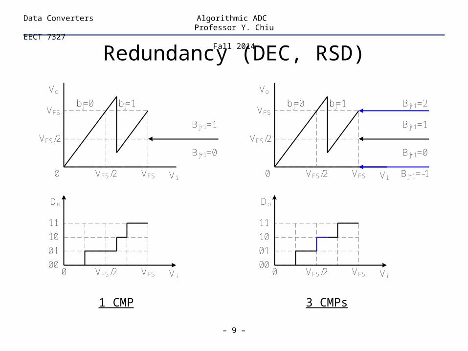
Redundancy (DEC, RSD)
– 9 –
Data Converters Algorithmic ADC Professor Y. Chiu
EECT 7327Fall 2014
Vi
Vo
VFS/20 VFS
VFSbj=0 bj=1
VFS/2
Bj+1=0
Bj+1=1
Vi
Do
VFS/20 VFS00
01
10
11
Vi
Vo
VFS/20 VFS
VFSbj=0 bj=1
VFS/2
Bj+1=0
Bj+1=1
Bj+1=-1
Bj+1=2
Vi
Do
VFS/20 VFS00
01
10
11
1 CMP 3 CMPs

Loop Transfer Function
– 10 –
Data Converters Algorithmic ADC Professor Y. Chiu
EECT 7327Fall 2014
Original w/ Redundancy
• Subtraction/addition both required to compute final sum
• 4-level (2-bit) DAC required instead of 2-level (1-bit) DAC
Vi
Vo
VFS/20 VFS
VFSb=0 b=1
Vi
Vo
VFS/20 VFS
b=0 b=1b=-1 b=2
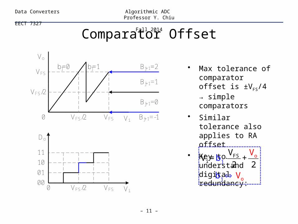
Comparator Offset
– 11 –
Data Converters Algorithmic ADC Professor Y. Chiu
EECT 7327Fall 2014
Vi
Vo
VFS/20 VFS
VFSbj=0 bj=1
VFS/2
Bj+1=0
Bj+1=1
Bj+1=-1
Bj+1=2
Vi
Do
VFS/20 VFS00
01
10
11
• Max tolerance of comparator offset is ±VFS/4 → simple comparators
• Similar tolerance also applies to RA offset
• Key to understand digital redundancy:
jo
o
i
j
FSVV = +
2b
2
V
V
b

Modified 1-Bit Architecture
– 12 –
Data Converters Algorithmic ADC Professor Y. Chiu
EECT 7327Fall 2014
1-b/s RA transfer curvew/ no redundancy
One extra CMPadded at VR/2
0
VR/2
-VR/2
Vi
Vo
-VR/2 VR/2-VR
VR
VR
0
VR/2
-VR/2
Vi
-VR/2 VR/2-VR
VR
VR
b=0 b=1 b=0 b=1b=0.5
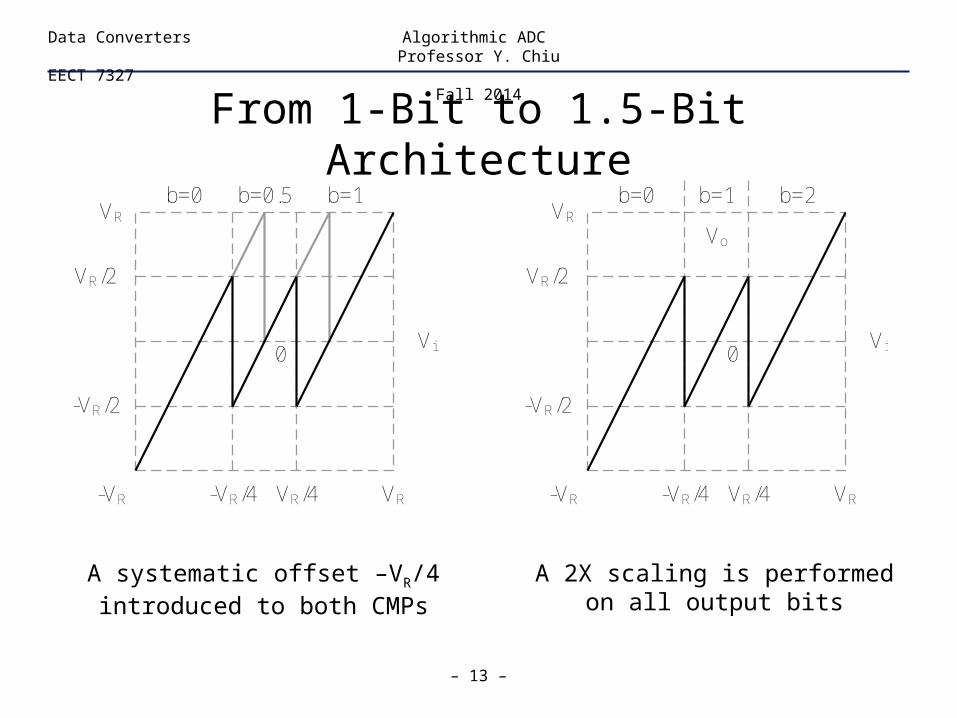
From 1-Bit to 1.5-Bit Architecture
– 13 –
Data Converters Algorithmic ADC Professor Y. Chiu
EECT 7327Fall 2014
-VR/4 VR/4
0
VR/2
-VR/2
Vi
-VR
VR
VR
b=0 b=1b=0.5
-VR/4 VR/4
0
VR/2
-VR/2
Vi
-VR
VR
VR
b=0 b=2b=1
Vo
A systematic offset –VR/4introduced to both CMPs
A 2X scaling is performedon all output bits

The 1.5-Bit Architecture
– 14 –
Data Converters Algorithmic ADC Professor Y. Chiu
EECT 7327Fall 2014
• 3 decision levels
→ ENOB = log23 = 1.58
• Max tolerance of comparator offset is ±VR/4
• An implementation of the Sweeny-Robertson-Tocher (SRT) division principle
• The conversion accuracy solely relies on the loop-gain error, i.e., the gain error and nonlinearity
• A 3-level DAC is required
Can this technique be applied to SA ADC?
-VR/4 VR/4
0
VR/2
-VR/2
Vi
-VR
VR
VR
b=0 b=2b=1
Vo
o i RV = 2 V - b -1 V
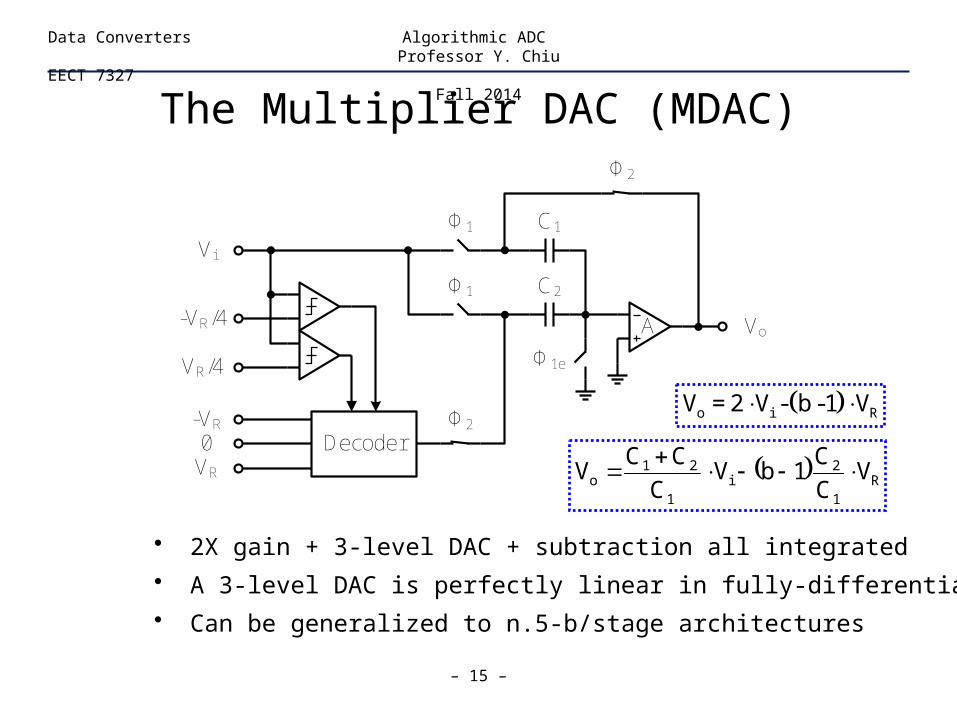
The Multiplier DAC (MDAC)
– 15 –
Data Converters Algorithmic ADC Professor Y. Chiu
EECT 7327Fall 2014
• 2X gain + 3-level DAC + subtraction all integrated
• A 3-level DAC is perfectly linear in fully-differential form
• Can be generalized to n.5-b/stage architectures
Vo
Vi
0-VR
VR
Decoder
Φ1 C1
Φ1 C2
Φ2
Φ1e
A
Φ2
-VR/4
VR/4
R1
2i
1
21o V
C
C1bV
C
CCV
o i RV = 2 V - b -1 V

A Linear 3-Level DAC
– 16 –
Data Converters Algorithmic ADC Professor Y. Chiu
EECT 7327Fall 2014
b = 0 b = 1 b = 2
Ri
TB1
2i
1
21
ooo
VV2
VVC
CV
C
CC
VVV
i
CMCM1
2i
1
21
ooo
V2
VVC
CV
C
CC
VVV
Ri
BT1
2i
1
21
ooo
VV2
VVC
CV
C
CC
VVV
Vo-
C1
C2
Vo+
C1
C2
AVT
VBVo-
C1
C2
Vo+
C1
C2
AVCM
VCM Vo-
C1
C2
Vo+
C1
C2
AVT
VB

Alternative 1.5-Bit Architecture
– 17 –
Data Converters Algorithmic ADC Professor Y. Chiu
EECT 7327Fall 2014
Ref: E. G. Soenen and R. L. Geiger, “An architecture and an algorithm for fully digital correction of monolithic pipelined ADC’s,” IEEE Trans. on Circuits and Systems II, vol. 42, issue 3, pp. 143-153, 1995.
-VR/2 VR/2
0Vi
-VR
VR
VR
b=0 b=2b=1
Vo
How does this work?
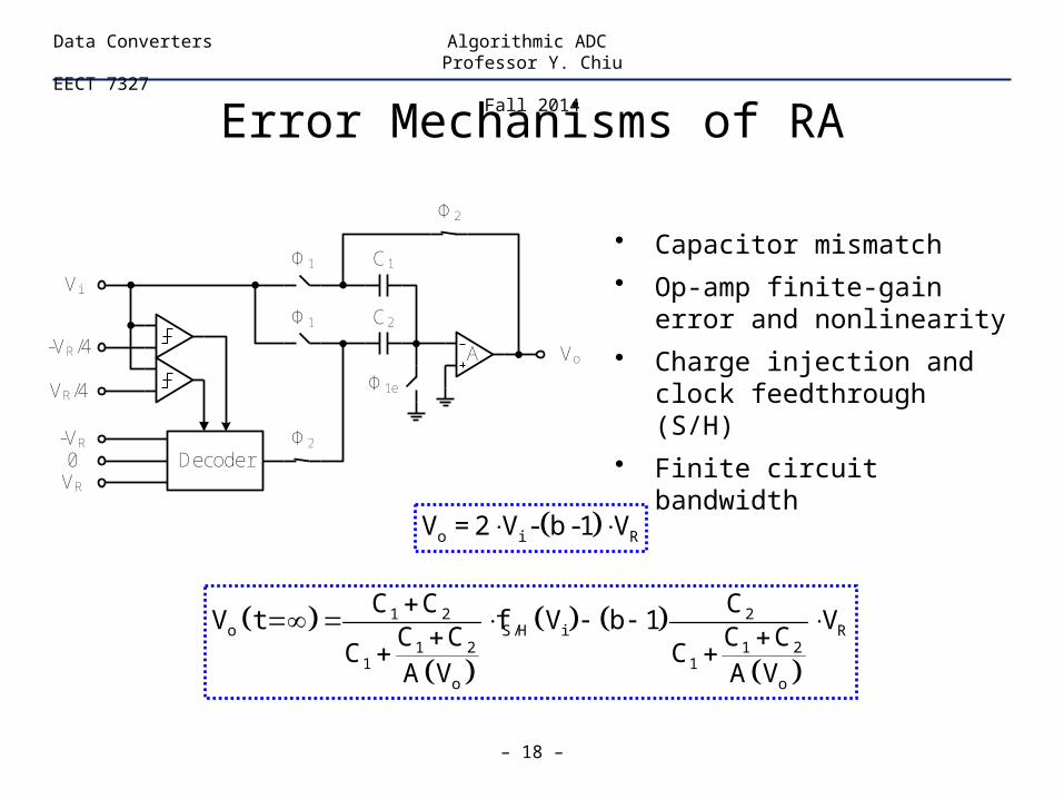
Error Mechanisms of RA
– 18 –
Data Converters Algorithmic ADC Professor Y. Chiu
EECT 7327Fall 2014
• Capacitor mismatch
• Op-amp finite-gain error and nonlinearity
• Charge injection and clock feedthrough (S/H)
• Finite circuit bandwidth
o i RV = 2 V - b -1 V
1 2 2o S/H i R
1 2 1 21 1
o o
C C CV t f V b 1 V
C C C CC C
A V A V
Vo
Vi
0-VR
VR
Decoder
Φ1 C1
Φ1 C2
Φ2
Φ1e
A
Φ2
-VR/4
VR/4

RA Gain Error and Nonlinearity
– 19 –
Data Converters Algorithmic ADC Professor Y. Chiu
EECT 7327Fall 2014
Raw accuracy is usually limited to 10-12 bits w/o error correction
-VR/4 VR/4
0
VR/2
-VR/2
Vi
-VR
VR
VR
b=0 b=2b=1
Vo
0Vi-VR VR
Do

Static Gain-Error Correction
– 20 –
Data Converters Algorithmic ADC Professor Y. Chiu
EECT 7327Fall 2014
1 2 2o i R i R
1 2 1 21 1
1 2
C C CV V b V V -b V
C Cka ka
C CC C
A A
1 2
1 21
oi 2i o
R 1 2 R 1 2
C CC VV CA b D = D + b
V C C V C Ckd kd
Analog-domain method:
Digital-domain method:
Do we need to correct for kd2 error?

RA Gain Trimming
– 21 –
Data Converters Algorithmic ADC Professor Y. Chiu
EECT 7327Fall 2014
• Precise gain-of-two is achieved by adjustment of the trim array
• Finite-gain error of op-amp is also compensated (not nonlinearity)
C1/C2 = 1 nominally
1 2o i
1 21
2R
1 21
C CV V
C CC
AC
b 1 VC C
CA
Vo-
Vo+
Vi+
Vi-
Trimarray
VX+
VX-
A
C1C2
C1C2

Split-Array Trimming DAC
– 22 –
Data Converters Algorithmic ADC Professor Y. Chiu
EECT 7327Fall 2014
• Successive approximation utilized to find the correct gain setting
• Coupling cap is slightly increased to ensure segmental overlap
2C1.2C
8C4C2CC8C4C2CC
2C1.2C
8C4C2CC8C4C2CC
VX+
VX-
Vi+
Vi-
8-bit gain1-bit sign

Digital Radix Correction
– 23 –
Data Converters Algorithmic ADC Professor Y. Chiu
EECT 7327Fall 2014
2 1
2 1 2 1
2 1
j j j+1
j j+1 j+2
2j j+1 j+2
2 3j j+1 j+2 j+3
2 3j j+1 j+2
2 1
2 1 2 1 2 1
2 1 j+32 1 2 1 2
kd kd
kd kd kd kd
kd kd kd kd
kd kd kd kd kd kd
kd kd kd kd
D = b + D
= b + b + D
= b + b + D
= b + b + b + D
= b + b + bkd kd kd+ b +...
1 2
1 21
oi 2i o
R 1 2 R 1 2
C CC VV CA b D = D + b
V C C V C Ckd kd
Unroll this:

References
– 24 –
Data Converters Algorithmic ADC Professor Y. Chiu
EECT 7327Fall 2014
1. P. W. Li, M. J. Chin, P. R. Gray, and R. Castello, JSSC, pp. 828-836, issue 6, 1984.
2. C. Shih and P. R. Gray, JSSC, pp. 544-554, issue 4, 1986.
3. H. Ohara et al., JSSC, pp. 930-938, issue 6, 1987.
4. H. Onodera, T. Tateishi, and K. Tamaru, JSSC, pp. 152-158, issue 1, 1988.
5. S. H. Lewis et al., JSSC, pp. 351-358, issue 3, 1992.
6. B. Ginetti et al., JSSC, pp. 957-964, issue 7, 1992.
7. H.-S. Lee, JSSC, pp. 509-515, issue 4, 1994.
8. S.-Y. Chin and C.-Y. Wu, JSSC, pp. 1201-1207, issue 8, 1996.
9. E. G. Soenen and R. L. Geiger, TCAS2, pp. 143-153, issue 3, 1995.
10. I. E. Opris, L. D. Lewicki, and B. C. Wong, JSSC, pp. 1898-1903, issue 12, 1998.
11. O. E. Erdogan, P. J. Hurst, and S. H. Lewis, JSSC, pp. 1812-1820, issue 12, 1999.